
DS8921/DS8921A/DS8921AT
Differential Line Driver and Receiver Pair
General Description
The DS8921, DS8921A are Differential Line Driver and Re-
ceiver pairs designed specifically for applications meeting
the ST506, ST412 and ESDI Disk Drive Standards. In addi-
tion, these devices meet the requirements of the EIA Stan-
dard RS-422.
The DS8921, DS8921A receivers offer an input sensitivity of
200 mV over a
±
7V common mode operating range. Hyster-
esis is incorporated (typically 70 mV) to improve noise mar-
gin for slowly changing input waveforms.
The DS8921, DS8921A drivers are designed to provide uni-
polar differential drive to twisted pair or parallel wire trans-
mission lines. Complementary outputs are logically ANDed
and provide an output skew of 0.5 ns (typ.) with propagation
delays of 12 ns.
The DS8921, DS8921A are designed to be compatible with
TTL and CMOS.
Features
n
12 ns typical propagation delay
n
Output skew - 0.5 ns typical
n
Meet the requirements of EIA Standard RS-422
n
Complementary Driver Outputs
n
High differential or common-mode input voltage ranges
of
±
7V
n
±
0.2V receiver sensitivity over the input voltage range
n
Receiver input hysteresis-70 mV typical
n
DS8921AT industrial temperature
operation: (−40˚C to +85˚C)
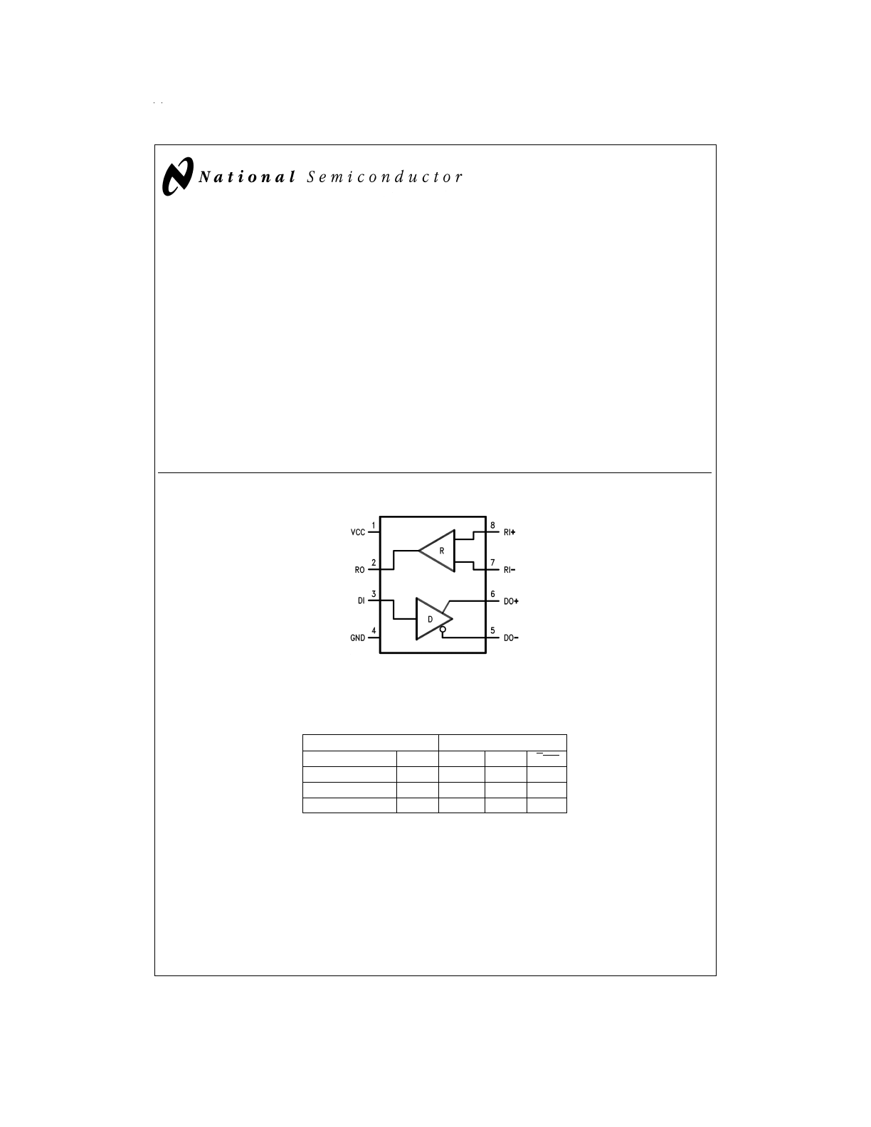
Connection Diagram
Truth Table
Receiver
Driver
Input
V
OUT
Input
V
OUT
V
OUT
V
ID
≥
V
TH
(MAX)
1
1
1
0
V
ID
≤
V
TH
(MIN)
0
0
0
1
Open
1
DS008512-1
Order Number DS8921M, DS8921N, DS8921AM, DS8921AN,
DS8921ATM, or DS8921ATN
See NS Package Number M08A or N08E
May 1998
DS8921/DS8921A/DS8921A
T
Differential
Line
Driver
and
Receiver
Pair
© 1998 National Semiconductor Corporation
DS008512
www.national.com
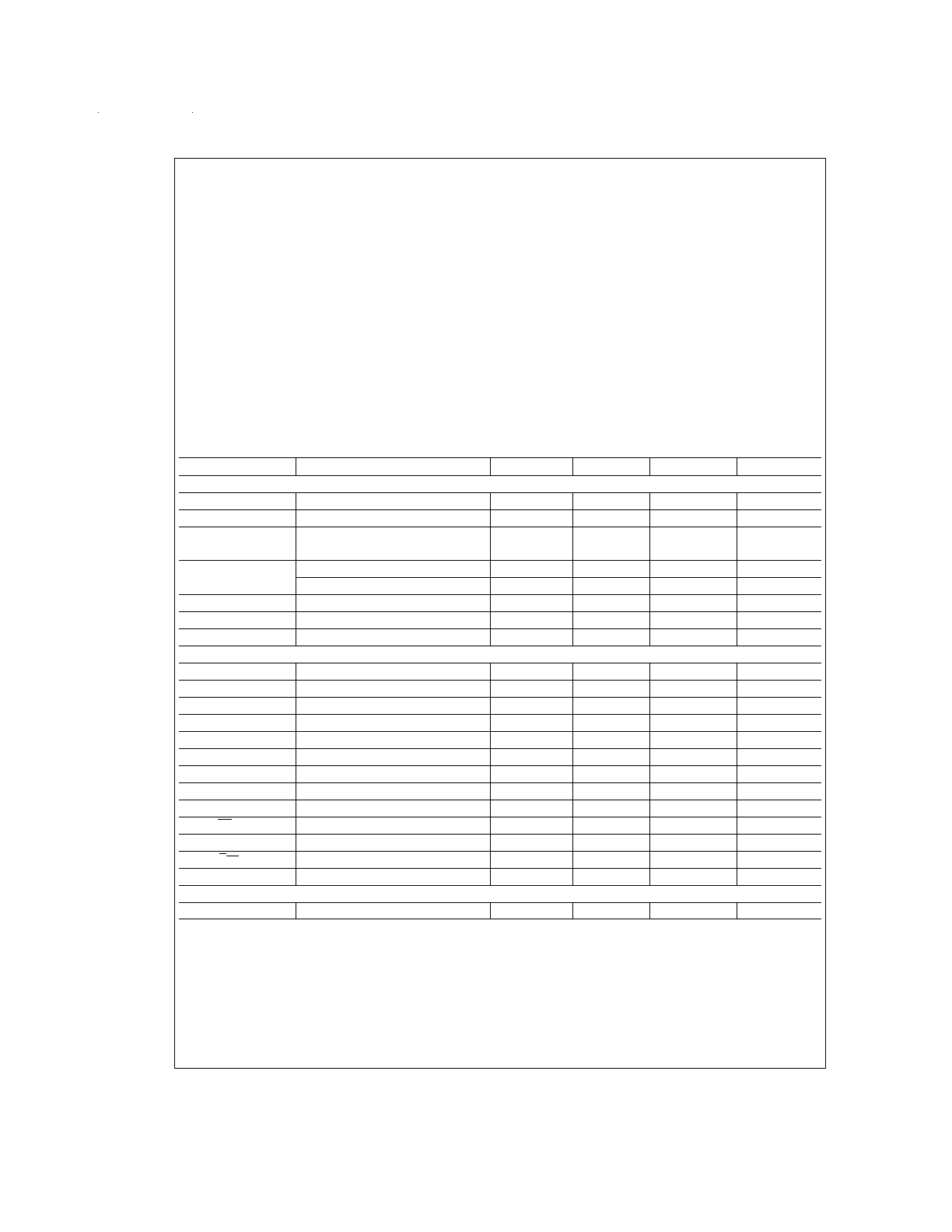
Absolute Maximum Ratings
(Note 1)
If Military/Aerospace specified devices are required,
please contact the National Semiconductor Sales Office/
Distributors for availability and specifications.
Supply Voltage
7V
Driver Input Voltage
−0.5V to +7V
Output Voltage
5.5V
Receiver Output Sink
Current
50 mA
Receiver Input Voltage
±
10V
Differential Input Voltage
±
12V
Maximum Package Power Dissipation
@
+25˚C
M Package
730 mW
N Package
1160 mW
Derate M Package
9.3 mW/˚C above +25˚C
Derate N Package
5.8 mW/˚C above +25˚C
Storage Temperature
Range
−65˚C to +165˚C
Lead Temperature
+260˚C
(Soldering, 4 sec.)
+260˚C
Maximum Junction
Temperature
+150˚C
Recommended Operating
Conditions
Min
Max
Units
Supply Voltage
4.5
5.5
V
Temperature (T
A
)
DS8921/DS8921A
0
70
˚C
DS8921AT
−40
+85
˚C
DS8921/DS8921A Electrical Characteristics
(Notes 2, 3, 4)
Symbol
Conditions
Min
Typ
Max
Units
RECEIVER
V
TH
−7V
≤
V
CM
≤
+7V
−200
±
35
+200
mV
V
HYST
−7V
≤
V
CM
≤
+7V
15
70
mV
R
IN
V
IN
= −7V, +7V
4.0
6.0
k
Ω
(Other Input = GND)
I
IN
V
IN
= 10V
3.25
mA
V
IN
= −10V
−3.25
mA
V
OH
I
OH
= −400 µA
2.5
V
V
OL
I
OL
= 8 mA
0.5
V
I
SC
V
CC
= MAX, V
OUT
= 0V
−15
−100
mA
DRIVER
V
IH
2.0
V
V
IL
0.8
V
I
IL
V
CC
= MAX, V
IN
= 0.4V
−40
−200
µA
I
IH
V
CC
= MAX, V
IN
= 2.7V
20
µA
I
I
V
CC
= MAX, V
IN
= 7.0V
100
µA
V
CL
V
CC
= MIN, I
IN
= −18 mA
−1.5
V
V
OH
V
CC
= MIN, I
OH
= −20 mA
2.5
V
V
OL
V
CC
= MIN, I
OL
= +20 mA
0.5
V
I
OFF
V
CC
= 0V, V
OUT
= 5.5V
100
µA
|V
T
| – |VT |
0.4
V
V
T
2.0
V
|V
OS
– V
OS
|
0.4
V
I
SC
V
CC
= MAX, V
OUT
= 0V
−30
−150
mA
DRIVER and RECEIVER
I
CC
V
CC
= MAX, V
OUT
= Logic 0
35
mA
www.national.com
2
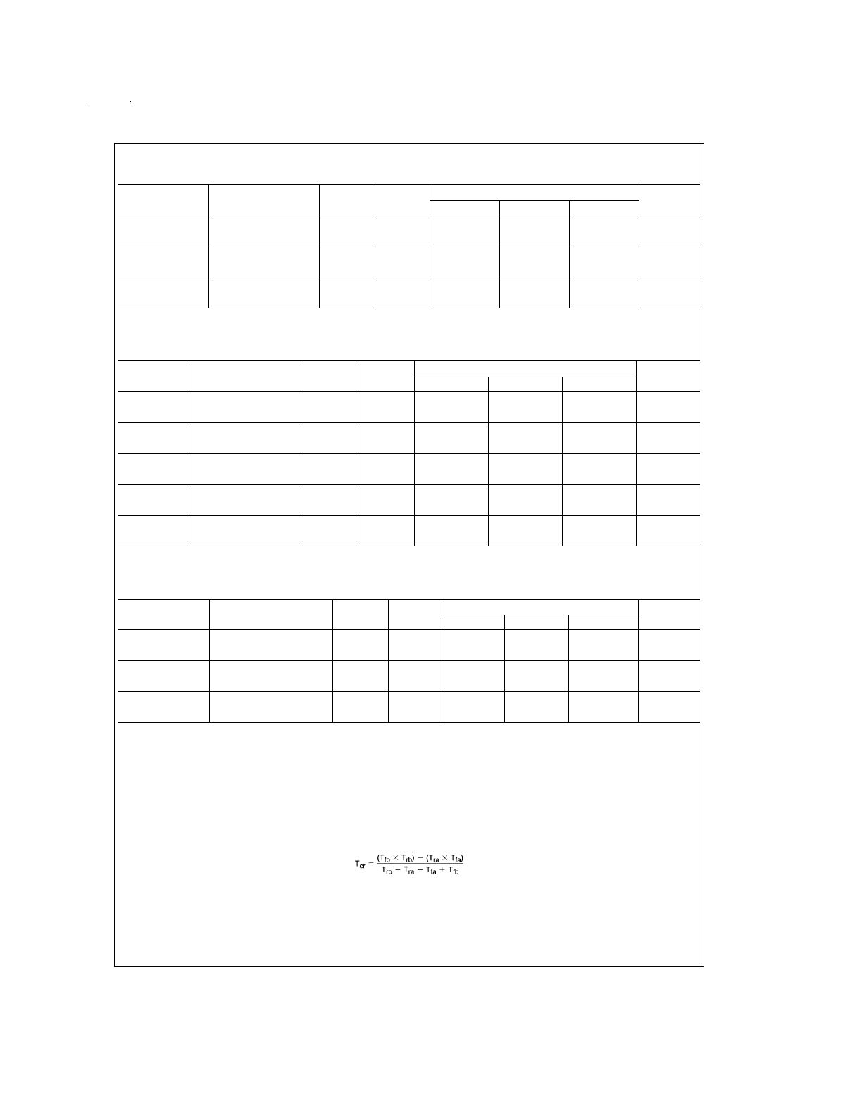
Receiver Switching Characteristics
Figure 1
(
Figure 2
)
Symbol
Conditions
Min
Typ
Max
Units
8921
8921A
8921AT
T
pLH
C
L
= 30 pF
14
22.5
20
20
ns
(
Figures 1, 2
)
T
pHL
C
L
= 30 pF
14
22.5
20
20
ns
(
Figures 1, 2
)
|T
pLH
–T
pHL
|
C
L
= 30 pF
0.5
5
3.5
5
ns
(
Figures 1, 2
)
Driver Switching Characteristics
SINGLE ENDED CHARACTERISTICS (
Figures 3, 4
)
Symbol
Conditions
Min
Typ
Max
Units
8921
8921A
8921AT
T
pLH
C
L
= 30 pF
10
15
15
15
ns
(
Figures 3, 4
)
T
pHL
C
L
= 30 pF
10
15
15
15
ns
(
Figures 3, 4
)
T
TLH
C
L
= 30 pF
5
8
8
9.5
ns
(
Figures 7, 8
)
T
THL
C
L
= 30 pF
5
8
8
9.5
ns
(
Figures 7, 8
)
Skew
CL = 30 pF
1
5
3.5
3.5
ns
(
Figures 3, 4
)
Driver Switching Characteristics
(Note 6)
DIFFERENTIAL CHARACTERISTICS (
Figures 3, 5
)
Symbol
Conditions
Min
Typ
Max
Units
8921
8921A
8921AT
T
pLH
C
L
= 30 pF
10
15
15
15
ns
(
Figures 3, 5, 6
)
T
pHL
C
L
= 30 pF
10
15
15
15
ns
(
Figures 3, 5, 6
)
|T
pLH
–T
pHL
|
C
L
= 30 pF
0.5
6
2.75
2.75
ns
(
Figures 3, 5, 6
)
Note 1: “Absolute Maximum Ratings” are those values beyond which the safety of the device cannot be guaranteed. They are not meant to imply that the device
should be operated at these limits. The Table of “Electrical Characteristics” provides conditions for actual device operation.
Note 2: All currents into device pins are shown as positive values; all currents out of the device are shown as negative; all voltages are referenced to ground unless
otherwise specified. All values shown as max or min are classified on absolute value basis.
Note 3: All typical values are V
CC
= 5V, T
A
= 25˚C.
Note 4: Only one output at a time should be shorted.
Note 5: Difference between complementary outputs at the 50% point.
Note 6: Differential Delays are defined as calculated results from single ended rise and fall time measurements. This approach in establishing AC performance speci-
fications has been taken due to limitations of available Automatic Test Equipment (ATE).
The calculated ATE results assume a linear transition between measurement points and are a result of the following equations:
Where: T
cr
= Crossing Point
T
ra
, T
rb
, T
fa
and T
fb
are time measurements with respect to the input. See
Figure 6
.
www.national.com
3
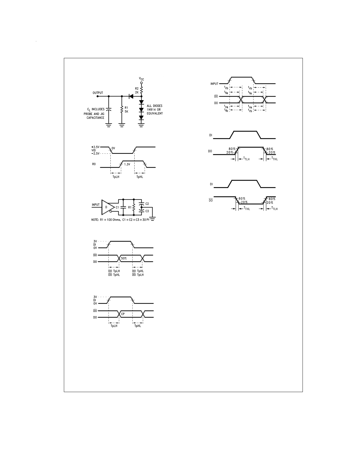
AC Test Circuits and Switching Diagrams
DS008512-3
FIGURE 1.
DS008512-4
FIGURE 2.
DS008512-5
FIGURE 3.
DS008512-6
FIGURE 4.
DS008512-7
FIGURE 5.
DS008512-2
FIGURE 6.
DS008512-10
FIGURE 7.
DS008512-11
FIGURE 8.
www.national.com
4
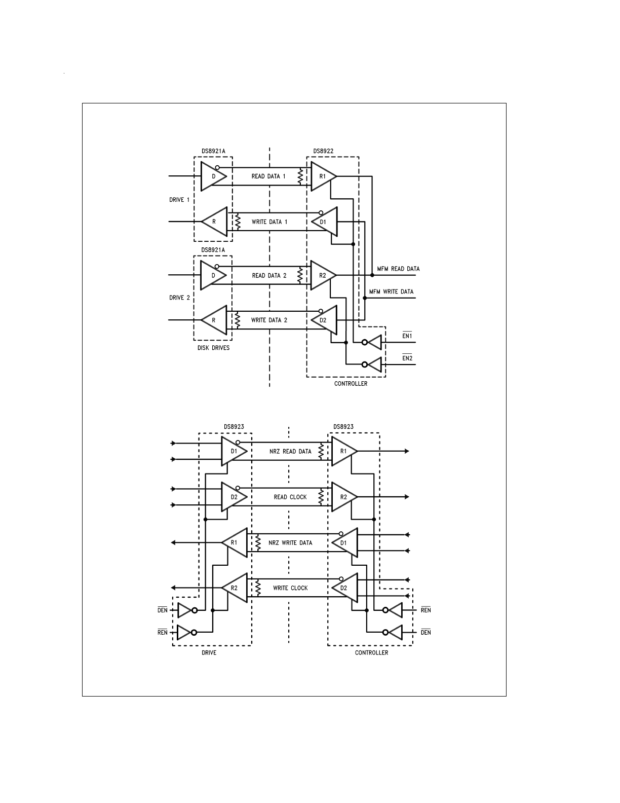
Typical Applications
ST506 and ST412 Application
DS008512-8
ESDI Application
DS008512-9
www.national.com
5

6
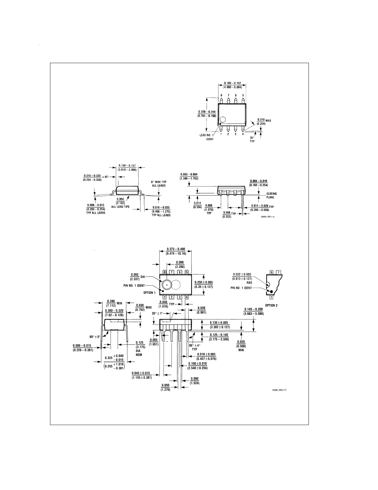
Physical Dimensions
inches (millimeters) unless otherwise noted
SO Package (M)
Order Number DS8921M, DS8921AM or DS8921ATM
NS Package Number M08A
Molded Dual-In-Line Package (N)
Order Number DS8921N, DS8921AN or DS8921ATN
NS Package Number N08E
www.national.com
7
LIFE SUPPORT POLICY
NATIONAL’S PRODUCTS ARE NOT AUTHORIZED FOR USE AS CRITICAL COMPONENTS IN LIFE SUPPORT DE-
VICES OR SYSTEMS WITHOUT THE EXPRESS WRITTEN APPROVAL OF THE PRESIDENT OF NATIONAL SEMI-
CONDUCTOR CORPORATION. As used herein:
1. Life support devices or systems are devices or sys-
tems which, (a) are intended for surgical implant into
the body, or (b) support or sustain life, and whose fail-
ure to perform when properly used in accordance
with instructions for use provided in the labeling, can
be reasonably expected to result in a significant injury
to the user.
2. A critical component in any component of a life support
device or system whose failure to perform can be rea-
sonably expected to cause the failure of the life support
device or system, or to affect its safety or effectiveness.
National Semiconductor
Corporation
Americas
Tel: 1-800-272-9959
Fax: 1-800-737-7018
Email: support@nsc.com
www.national.com
National Semiconductor
Europe
Fax: +49 (0) 1 80-530 85 86
Email: europe.support@nsc.com
Deutsch Tel: +49 (0) 1 80-530 85 85
English
Tel: +49 (0) 1 80-532 78 32
Français Tel: +49 (0) 1 80-532 93 58
Italiano
Tel: +49 (0) 1 80-534 16 80
National Semiconductor
Asia Pacific Customer
Response Group
Tel: 65-2544466
Fax: 65-2504466
Email: sea.support@nsc.com
National Semiconductor
Japan Ltd.
Tel: 81-3-5620-6175
Fax: 81-3-5620-6179
DS8921/DS8921A/DS8921A
T
Differential
Line
Driver
and
Receiver
Pair
National does not assume any responsibility for use of any circuitry described, no circuit patent licenses are implied and National reserves the right at any time without notice to change said circuitry and specifications.