
DS3695/DS3695T/DS3696/DS3697
Multipoint RS485/RS422 Transceivers/Repeaters
General Description
The DS3695, DS3696, and DS3697 are high speed differen-
tial TRI-STATE
®
bus/line transceivers/repeaters designed to
meet the requirements of EIA standard RS485 with extended
common mode range (+12V to −7V), for multipoint data
transmission.
The driver and receiver outputs feature TRI-STATE capabil-
ity. The driver outputs remain in TRI-STATE over the entire
common mode range of +12V to −7V. Bus faults that cause
excessive power dissipation within the device trigger a ther-
mal shutdown circuit, which forces the driver outputs into the
high impedance state. The DS3696 provides an output pin
TS (thermal shutdown) which reports the occurrence of the
thermal shutdown of the device. This is an “open collector”
pin with an internal 10 k
Ω
pull-up resistor. This allows the line
fault outputs of several devices to be wire OR-ed.
Both AC and DC specifications are guaranteed over the 0˚C
to 70˚C temperature and 4.75V to 5.25V supply voltage
range.
Features
n
Meets EIA standard RS485 for multipoint bus
transmission and is compatible with RS-422
n
15 ns driver propagation delays with 2 ns skew (typical)
n
Single +5V supply
n
−7V to +12V bus common mode range permits
±
7V
ground difference between devices on the bus
n
Thermal shutdown protection
n
High impedance to bus with driver in TRI-STATE or with
power off, over the entire common mode range allows
the unused devices on the bus to be powered down
n
Combined impedance of a driver output and receiver
input is less than one RS485 unit load, allowing up to 32
transceivers on the bus
n
70 mV typical receiver hysteresis
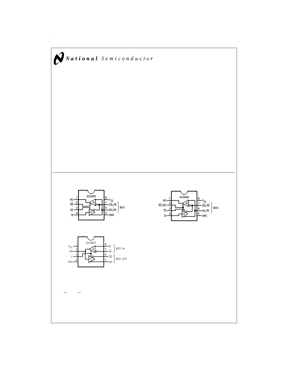
Connection and Logic Diagrams
Note 1: TS pin was LF (Line Fault) in previous datasheets and reports the occurrence of a thermal shutdown of the device.
TRI-STATE
®
is a registered trademark of National Semiconductor Corporation.
DS010408-1
Top View
DS010408-12
Top View
DS010408-13
Top View
Order Number DS3695N, DS3695TN,
DS3696N, or DS3697N
See NS Package Number N08E
May 1998
DS3695/DS3695T/DS3696/DS3697
Multipoint
RS485/RS422
T
ransceivers/Repeaters
© 1998 National Semiconductor Corporation
DS010408
www.national.com
Absolute Maximum Ratings
(Note 2)
If Military/Aerospace specified devices are required,
please contact the National Semiconductor Sales Office/
Distributors for availability and specifications.
Supply Voltage, V
CC
7V
Control Input Voltages
7V
Driver Input Voltage
7V
Driver Output Voltages
+15V/−10V
Receiver Input Voltages
(DS3695, DS3696)
+15V/−10V
Receiver Common Mode Voltage
(DS3697)
±
25V
Receiver Output Voltage
5.5V
Continuous Power Dissipation
@
25˚C
N Package
1.07W (Note
4)
Storage Temperature Range
−65˚C to
+150˚C
Lead Temperature (Soldering, 4
sec.)
260˚C
Recommended Operating
Conditions
Min
Max
Units
Supply Voltage, V
CC
4.75
5.25
V
Bus Voltage
−7
+12
V
Operating Free Air Temp. (T
A
)
Commercial
0
+70
˚C
Industrial
−40
+85
˚C
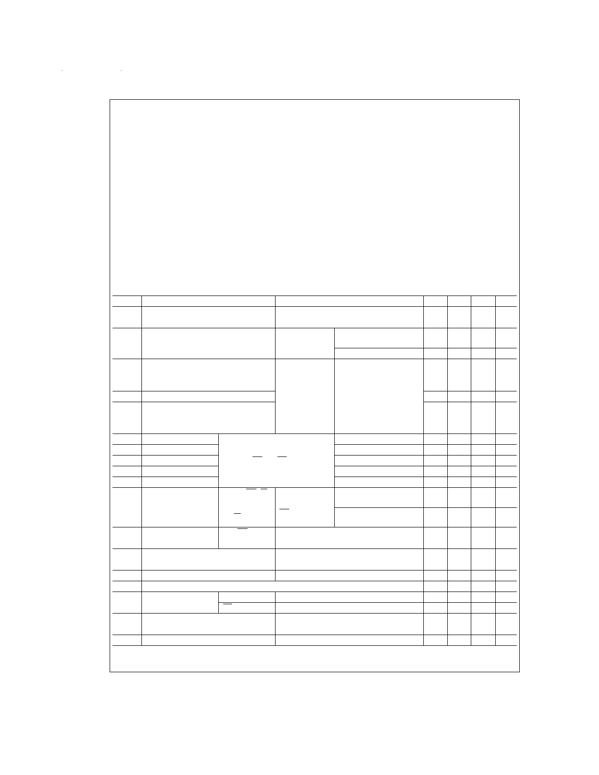
Electrical Characteristics
(Notes 3, 4)
0˚C
≤
T
A
≤
+70˚C, 4.75V
<
V
CC
<
5.25V unless otherwise specified
Symbol
Parameter
Conditions
Min
Typ
Max
Units
V
OD1
Differential Driver Output
I
O
= 0
5
V
Voltage (Unloaded)
V
OD2
Differential Driver Output
(
Figure 1
)
R = 50
Ω
; (RS-422) (Note
6)
2
V
Voltage (with Load)
R = 27
Ω
; (RS-485)
1.5
V
∆
V
OD
Change in Magnitude of Driver
Differential Output Voltage for
0.2
V
Complementary Output States
V
OC
Driver Common Mode Output Voltage
(
Figure 1
)
R = 27
Ω
3.0
V
∆
|V
OC
|
Change in Magnitude of Driver
Common Mode Output Voltage
0.2
V
for Complementary Output States
V
IH
Input High Voltage
2
V
V
IL
Input Low Voltage
DI, DE,
0.8
V
V
CL
Input Clamp Voltage
RE , E, RE /DE
I
IN
= −18 mA
−1.5
V
I
IL
Input Low Current
V
IL
= 0.4V
−200
µA
I
IH
Input High Current
V
IH
= 2.4V
20
µA
I
IN
Input Current
DO/RI, DO /RI
V
CC
= 0V or
5.25V
V
IN
= 12V
+1.0
mA
RI, RI
RE /DE or DE =
0V
V
IN
= −7V
−0.8
mA
I
OZD
TRI-STATE Current
DO, DO
V
CC
= 0V or 5.25V, E = 0V
±
100
µA
DS3697 & DS3698
−7V
<
V
O
<
+12V
V
TH
Differential Input Threshold
−7V
≤
V
CM
≤
+12V
−0.2
+0.2
V
Voltage for Receiver
∆
V
TH
Receiver Input Hysteresis
V
CM
= 0V
70
mV
V
OH
Receiver Output High Voltage
I
OH
= −400 µA
2.4
V
V
OL
Output Low Voltage
RO
I
OL
= 16 mA (Note 6)
0.5
V
TS
I
OL
= 8 mA
0.45
V
I
OZR
OFF-State (High Impedance)
V
CC
= Max
±
20
µA
Output Current at Receiver
0.4V
≤
V
O
≤
2.4V
R
IN
Receiver Input Resistance
−7V
≤
V
CM
≤
+12V
12
k
Ω
www.national.com
2
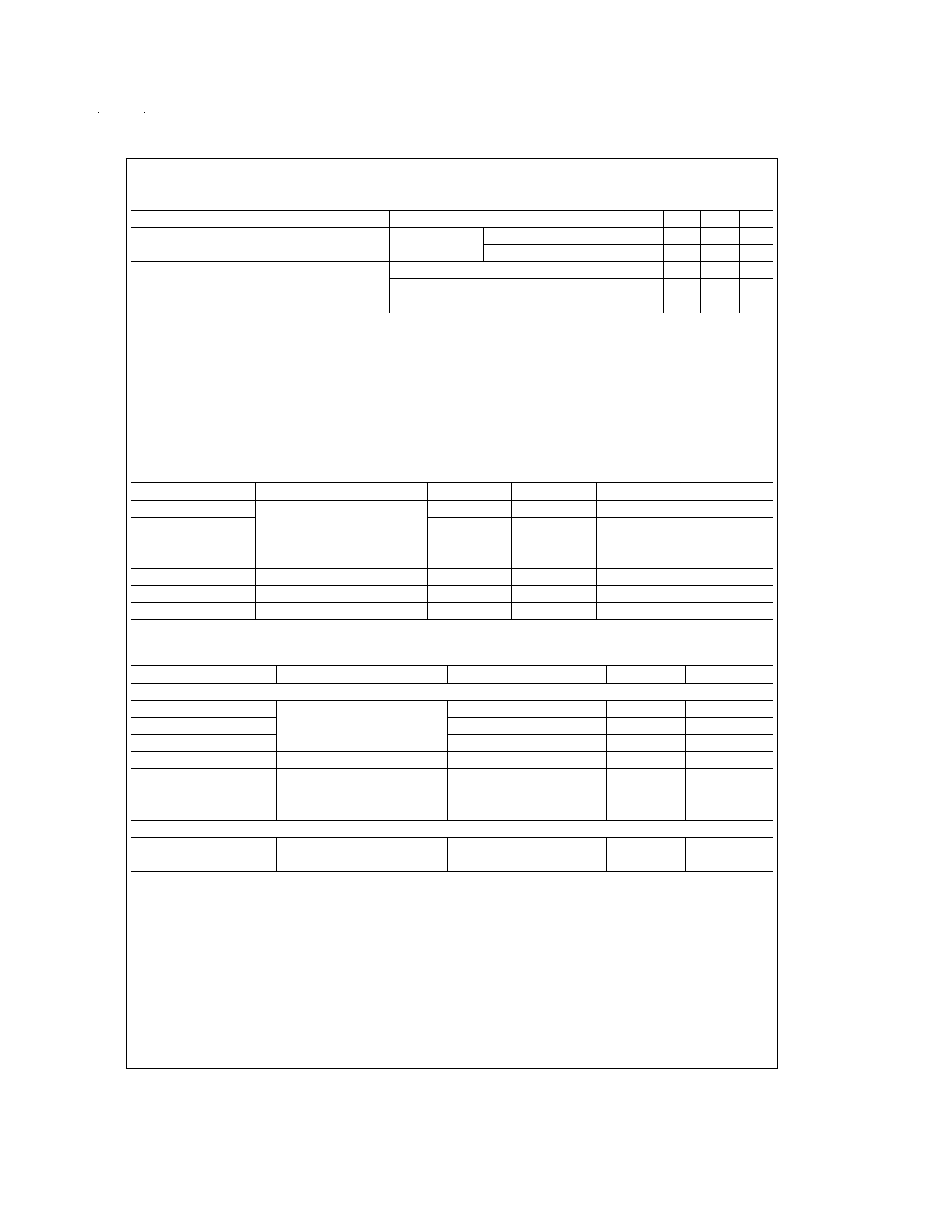
Electrical Characteristics
(Notes 3, 4) (Continued)
0˚C
≤
T
A
≤
+70˚C, 4.75V
<
V
CC
<
5.25V unless otherwise specified
Symbol
Parameter
Conditions
Min
Typ
Max
Units
I
CC
Supply Current
No Load
Driver Outputs Enabled
42
60
mA
(Note 6)
Driver Outputs Disabled
27
40
mA
I
OSD
Driver Short-Circuit Output Current
V
O
= −7V (Note 6)
−250
mA
V
O
= +12V (Note 6)
+250
mA
I
OSR
Receiver Short-Circuit Output Current
V
O
= 0V
−15
−85
mA
Note 2: “Absolute Maximum Ratings” are those beyond which the safety of the device cannot be guaranteed. They are not meant to imply that the device should
be operated at these limits. The tables of “Electrical Characteristics” provide conditions for actual device operation.
Note 3: All currents into device pins are positive; all currents out of device pins are negative. All voltages are referenced to device ground unless otherwise specified.
Note 4: All typicals are given for V
CC
= 5V and T
A
= 25˚C.
Note 5: Derate linearly at 11.1 mW/˚C to 570 mW at 70˚C.
Note 6: All limits for which Note 5 is applied must be derated by 10% for DS3695T and DS3696T. Other parameters remain the same for this extended temperature
range device (−40˚C
≤
T
A
≤
+85˚C).
Switching Characteristics
(Notes 4, 7) 0˚C
≤
T
A
≤
+70˚C, 4.75V
<
V
CC
<
5.25V unless otherwise specified
Receiver Switching Characteristics
(
Figures 2, 3, 4
)
Symbol
Conditions
Min
Typ
Max
Units
t
PLH
C
L
= 15 pF
15
25
37
ns
t
PHL
S1 and S2
15
25
37
ns
|t
PLH
–t
PHL
|
Closed
0
ns
t
PLZ
C
L
= 15 pF, S2 Open
5
12
16
ns
t
PHZ
C
L
= 15 pF, S1 Open
5
12
16
ns
t
PZL
C
L
= 15 pF, S2 Open
7
15
20
ns
t
PZH
C
L
= 15 pF, S1 Open
7
15
20
ns
Driver Switching Characteristics
Symbol
Conditions
Min
Typ
Max
Units
SINGLE ENDED CHARACTERISTICS (
Figures 5, 6, 7
)
t
PLH
R
L
DIFF = 60
Ω
9
15
22
ns
t
PHL
C
L1
= C
L2
= 100 pF
9
15
22
ns
t
SKEW
|t
PLH
–t
PHL
|
2
8
ns
t
PLZ
C
L
= 15 pF, S2 Open
7
15
30
ns
t
PHZ
C
L
= 15 pF, S1 Open
7
15
30
ns
t
PZL
C
L
= 100 pF, S2 Open
30
35
50
ns
t
PZH
C
L
= 100 pF, S1 Open
30
35
50
ns
DIFFERENTIAL CHARACTERISTICS (
Figures 5, 8
)
t
r
, t
f
R
L
DIFF = 60
Ω
6
10
18
ns
C
L1
= C
L2
= 100 pF
Note 7: Switching Characteristics apply for DS3695, DS3695T, DS3696, DS3697 only.
www.national.com
3
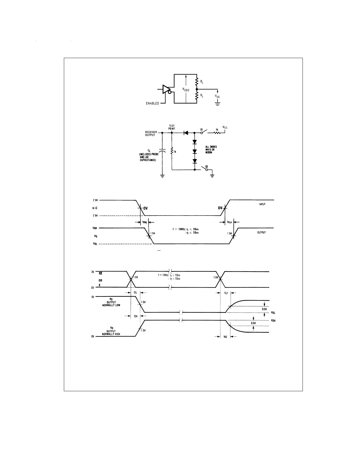
AC Test Circuits and Switching Waveforms
DS010408-15
FIGURE 1. Driver V
OD
and V
OC
DS010408-3
FIGURE 2. Receiver Propagation Delay Test Circuit
DS010408-4
Note: Differential input voltage may be realized by grounding RI and pulsing RI between +2.5V and −2.5V.
FIGURE 3. Receiver Input-to-Output Propagation Delay Timing
DS010408-5
FIGURE 4. Receiver Enable/Disable Propagation Delay Timing
www.national.com
4
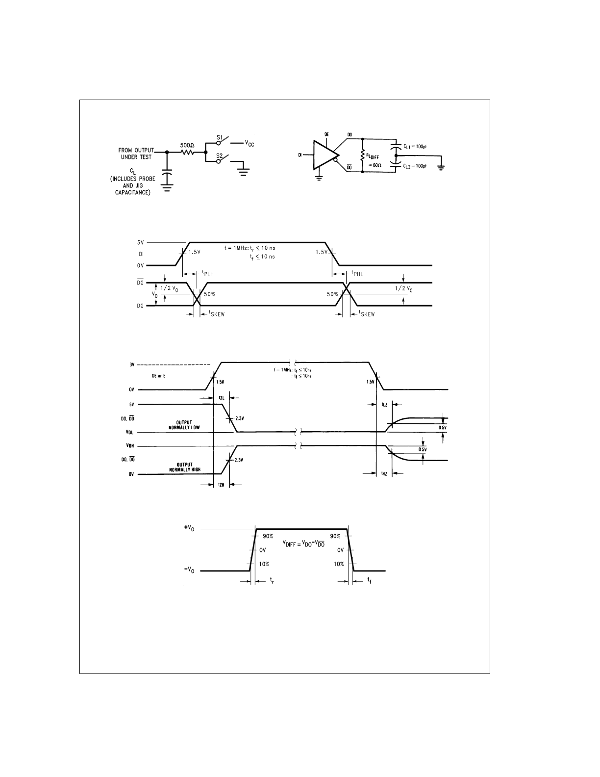
AC Test Circuits and Switching Waveforms
(Continued)
DS010408-6
Note: Unless otherwise specified the switches are closed.
DS010408-7
FIGURE 5. Driver Propagation Delay and Transition Time Test Circuits
DS010408-8
Note: t
PLH
and t
PHL
are measured to the respective 50% points. t
SKEW
is the difference between propagation delays of the complementary outputs.
FIGURE 6. Driver Input-to-Output Propagation Delay Timing (Single-Ended)
DS010408-9
FIGURE 7. Driver Enable/Disable Propagation Delay Timing
DS010408-10
FIGURE 8. Driver Differential Transition Timing
www.national.com
5
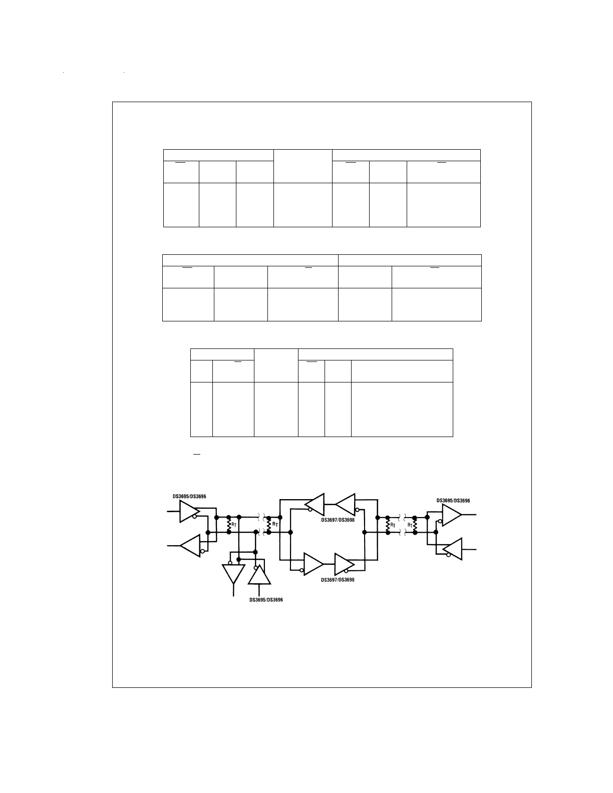
Function Tables
DS3695/DS3696 Transmitting
Inputs
Thermal
Outputs
RE
DE
DI
Shutdown
DO
DO
TS
*
(DS3696 Only)
X
1
1
OFF
0
1
H
X
1
0
OFF
1
0
H
X
0
X
OFF
Z
Z
H
X
1
X
ON
Z
Z
L
DS3695/DS3696 Receiving
Inputs
Outputs
RE
DE
RI–RI
RO
TS
*
(DS3696 Only)
0
0
≥
+0.2V
1
H
0
0
≤
−0.2V
0
H
1
0
X
Z
H
DS3697
Inputs
Thermal
Outputs
E
RI-RI
Shutdown
DO
DO
RO
(DS3697 Only)
1
≥
+0.2V
OFF
0
1
1
1
≤
−0.2V
OFF
1
0
0
0
X
OFF
Z
Z
Z
1
≥
+0.2V
ON
Z
Z
1
1
≤
−0.2V
ON
Z
Z
0
X — Don’t care condition
Z — High impedance state
*
TS is an “open collector” output with an on-chip 10 k
Ω
pull-up resistor that reports the occurrence of a thermal shutdown of the device.
Typical Application
DS010408-11
Note: Repeater control logic not shown, see AN-702.
www.national.com
6
Typical Performance Characteristics
Driver V
OH
vs
I
OH
vs Temperature
DS010408-19
Driver V
OH
vs I
OH
vs V
CC
Driver
V
OH
vs I
OH
vs V
CC
DS010408-20
Driver V
OL
vs
I
OL
vs Temperature
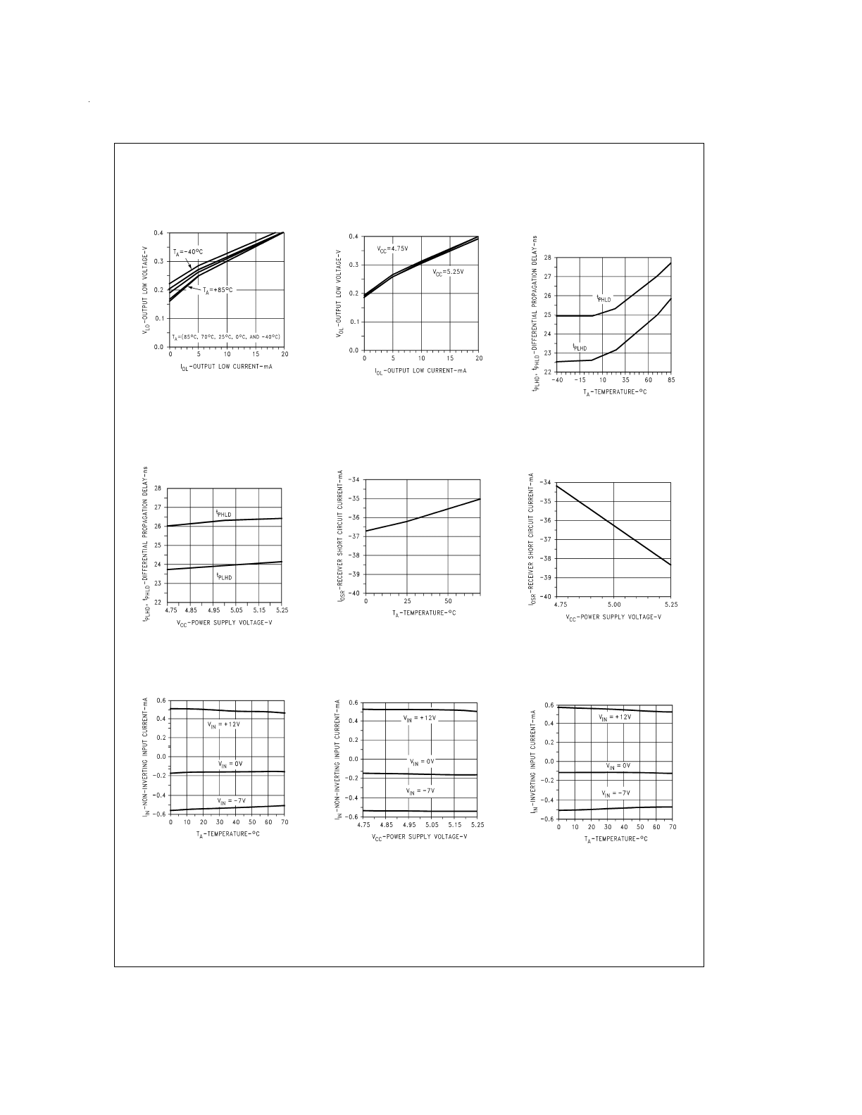
DS010408-21
Driver V
OH
vs I
OH
vs V
CC
DS010408-22
Driver Differential
Propagation
Delay vs Temperature
DS010408-23
Driver Differential Propagation
Delay vs V
CC
DS010408-24
Driver Single-Ended Propagation
Delay vs Temperature
DS010408-25
Driver Single-Ended Propagation
Delay vs V
CC
DS010408-26
Driver Transition Time
vs Temperature
DS010408-27
www.national.com
7
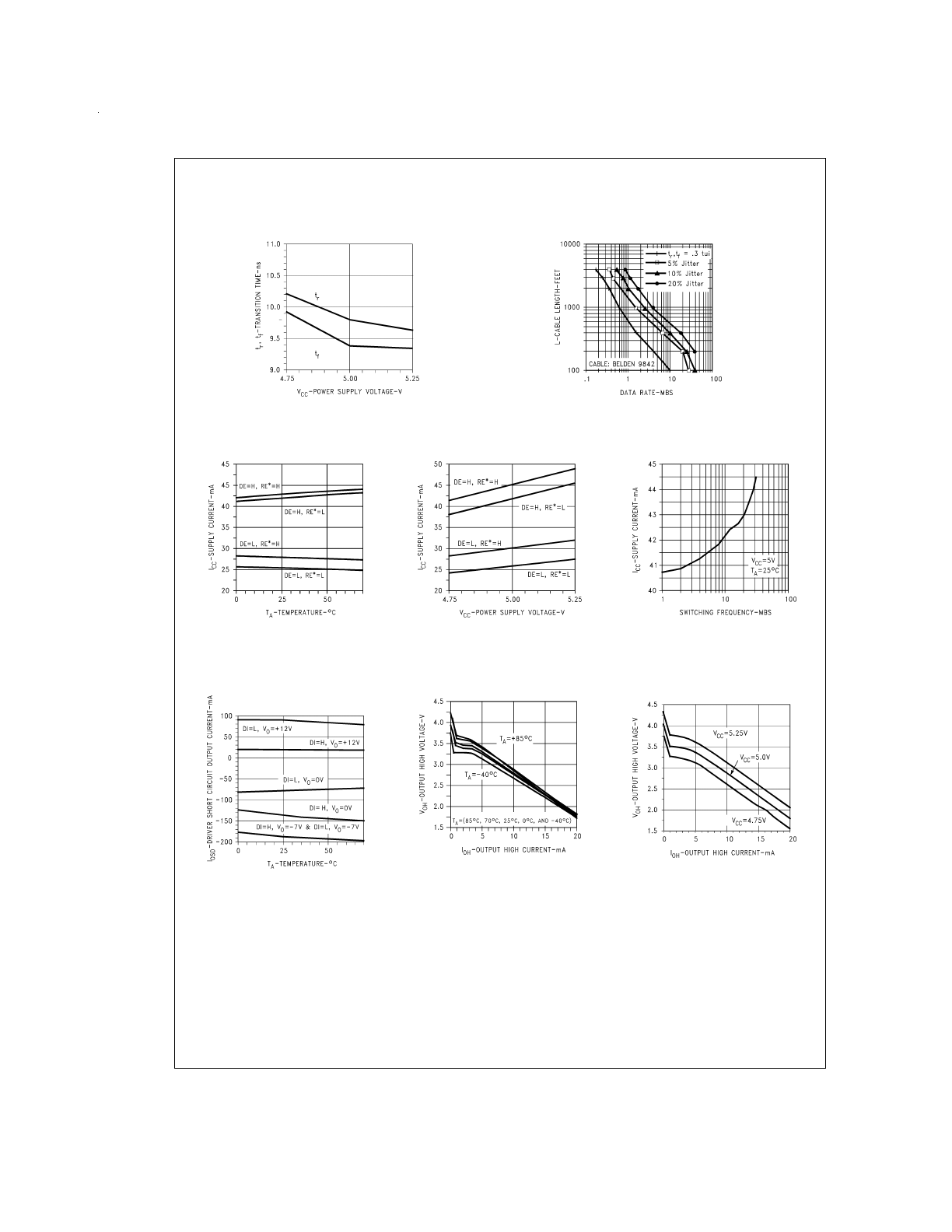
Typical Performance Characteristics
(Continued)
Driver Transition Time
vs V
CC
DS010408-28
Cable Length vs Data Rate
DS010408-29
Supply Current vs
Temperature
DS010408-30
Supply Current vs Power
Supply Voltage
DS010408-31
Driver I
CC
vs Switching
Frequency
DS010408-32
Driver Short
Circuit Current
vs Temperature
DS010408-33
Receiver V
OH
vs I
OH
vs Temperature
DS010408-34
Receiver V
OH
vs
I
OH
vs V
CC
DS010408-35
www.national.com
8
Typical Performance Characteristics
(Continued)
Receiver V
OL
vs I
OL
vs Temperature
DS010408-36
Receiver V
OL
vs
I
OL
vs V
CC
DS010408-37
Receiver Differential
Propagation Delay
vs Temperature
DS010408-38
Receiver Differential
Propagation Delay
vs V
CC
DS010408-39
Receiver Short
Circuit Current
vs Temperature
DS010408-40
Receiver Short
Circuit Current
vs Power Supply
DS010408-41
Receiver Non-Inverting
Input Current
vs Temperature
DS010408-42
Receiver Non-Inverting
Input Current vs
Power Supply Voltage
DS010408-43
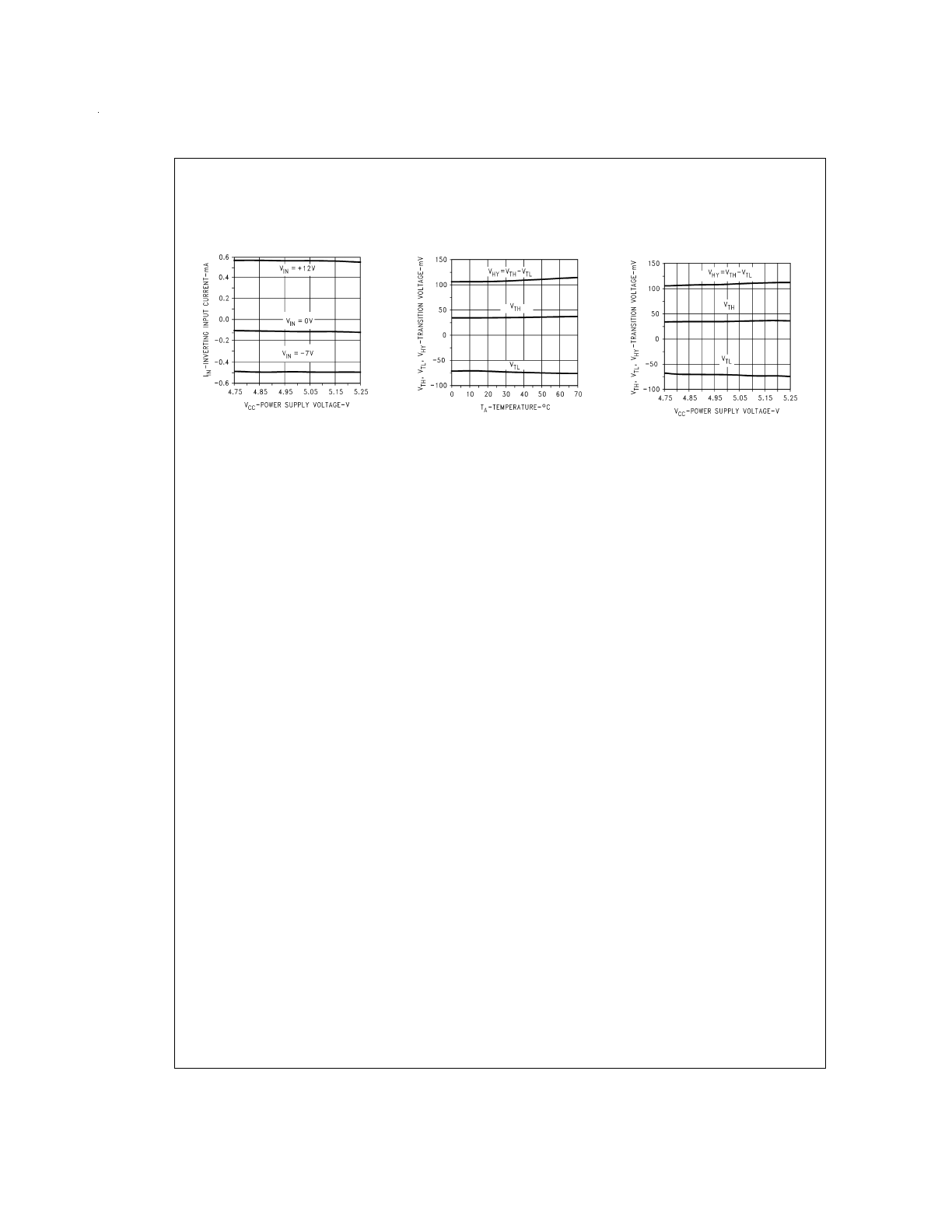
Receiver Inverting
Input Current
vs Temperature
DS010408-44
www.national.com
9
Typical Performance Characteristics
(Continued)
Receiver Inverting
Input Current vs
Power Supply Voltage
DS010408-45
Hysteresis and Differential
Transition Voltage
vs Temperature
DS010408-46
Hysteresis and
Differential Transition
Voltage vs V
CC
DS010408-47
www.national.com
10

11
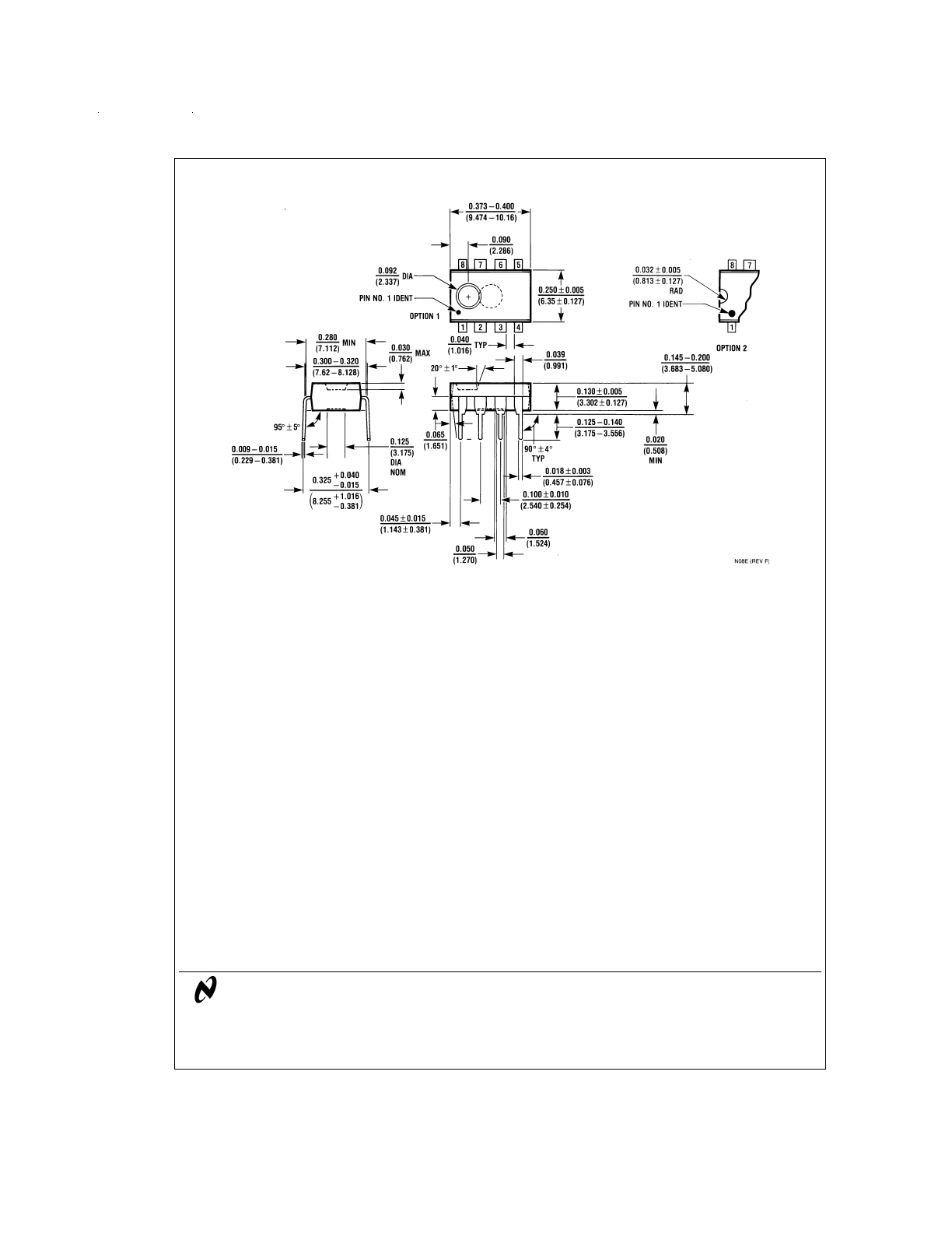
Physical Dimensions
inches (millimeters) unless otherwise noted
LIFE SUPPORT POLICY
NATIONAL’S PRODUCTS ARE NOT AUTHORIZED FOR USE AS CRITICAL COMPONENTS IN LIFE SUPPORT DE-
VICES OR SYSTEMS WITHOUT THE EXPRESS WRITTEN APPROVAL OF THE PRESIDENT OF NATIONAL SEMI-
CONDUCTOR CORPORATION. As used herein:
1. Life support devices or systems are devices or sys-
tems which, (a) are intended for surgical implant into
the body, or (b) support or sustain life, and whose fail-
ure to perform when properly used in accordance
with instructions for use provided in the labeling, can
be reasonably expected to result in a significant injury
to the user.
2. A critical component in any component of a life support
device or system whose failure to perform can be rea-
sonably expected to cause the failure of the life support
device or system, or to affect its safety or effectiveness.
National Semiconductor
Corporation
Americas
Tel: 1-800-272-9959
Fax: 1-800-737-7018
Email: support@nsc.com
www.national.com
National Semiconductor
Europe
Fax: +49 (0) 1 80-530 85 86
Email: europe.support@nsc.com
Deutsch Tel: +49 (0) 1 80-530 85 85
English
Tel: +49 (0) 1 80-532 78 32
Français Tel: +49 (0) 1 80-532 93 58
Italiano
Tel: +49 (0) 1 80-534 16 80
National Semiconductor
Asia Pacific Customer
Response Group
Tel: 65-2544466
Fax: 65-2504466
Email: sea.support@nsc.com
National Semiconductor
Japan Ltd.
Tel: 81-3-5620-6175
Fax: 81-3-5620-6179
8-Lead Molded Dual-In-Line Package (N)
Order Number DS3695N, DS3696N, DS3697N, or DS3695TN
NS Package Number N08E
DS3695/DS3695T/DS3696/DS3697
Multipoint
RS485/RS422
T
ransceivers/Repeaters
National does not assume any responsibility for use of any circuitry described, no circuit patent licenses are implied and National reserves the right at any time without notice to change said circuitry and specifications.