
DS26LS32C/DS26LS32M/DS26LS32AC/DS26LS33C/
DS26LS33M/DS26LS33AC
Quad Differential Line Receivers
General Description
The DS26LS32 and DS26LS32A are quad differential line re-
ceivers designed to meet the RS-422, RS-423 and Federal
Standards 1020 and 1030 for balanced and unbalanced digi-
tal data transmission.
The DS26LS32 and DS26LS32A have an input sensitivity of
200 mV over the input voltage range of
±
7V and the
DS26LS33 and DS26LS33A have an input sensitivity of
500 mV over the input voltage range of
±
15V.
Both the DS26LS32A and DS26LS33A differ in function from
the popular DS26LS32 and DS26LS33 in that input pull-up
and pull-down resistors are included which prevent output
oscillation on unused channels.
Each version provides an enable and disable function com-
mon to all four receivers and features TRI-STATE
®
outputs
with 8 mA sink capability. Constructed using low power
Schottky processing, these devices are available over the
full military and commerical operating temperature ranges.
Features
n
High differential or common-mode input voltage ranges
of
±
7V on the DS26LS32 and DS26LS32A and
±
15V
on the DS26LS33 and DS26LS33A
n
±
0.2V sensitivity over the input voltage range on the
DS26LS32 and DS26LS32A,
±
0.5V sensitivity on the
DS26LS33 and DS26LS33A
n
DS26LS32 and DS26LS32A meet all requirements of
RS-422 and RS-423
n
6k minimum input impedance
n
100 mV input hysteresis on the DS26LS32 and
DS26LS32A, 200 mV on the DS26LS33 and
DS26LS33A
n
Operation from a single 5V supply
n
TRI-STATE outputs, with choice of complementary
output enables for receiving directly onto a data bus
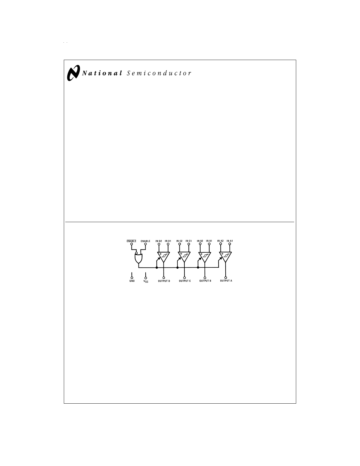
Logic Diagram
TRI-STATE
®
is a registered trademark of National Semiconductor Corporation.
DS005255-1
December 1998
DS26LS32C/DS26LS32M/DS26LS32AC/DS26LS33C/DS26LS33M/DS26LS33AC
Quad
Differential
Line
Receivers
© 1998 National Semiconductor Corporation
DS005255
www.national.com
Connection Diagram
Truth Table
ENABLE
ENABLE
Input
Output
0
1
X
Hi-Z
See
V
ID
≥
V
TH
(Max)
1
Note Below
V
ID
≤
V
TH
(Min)
0
Hi-Z = TRI-STATE
®
Note: Input conditions may be any combination not defined for ENABLE and ENABLE .
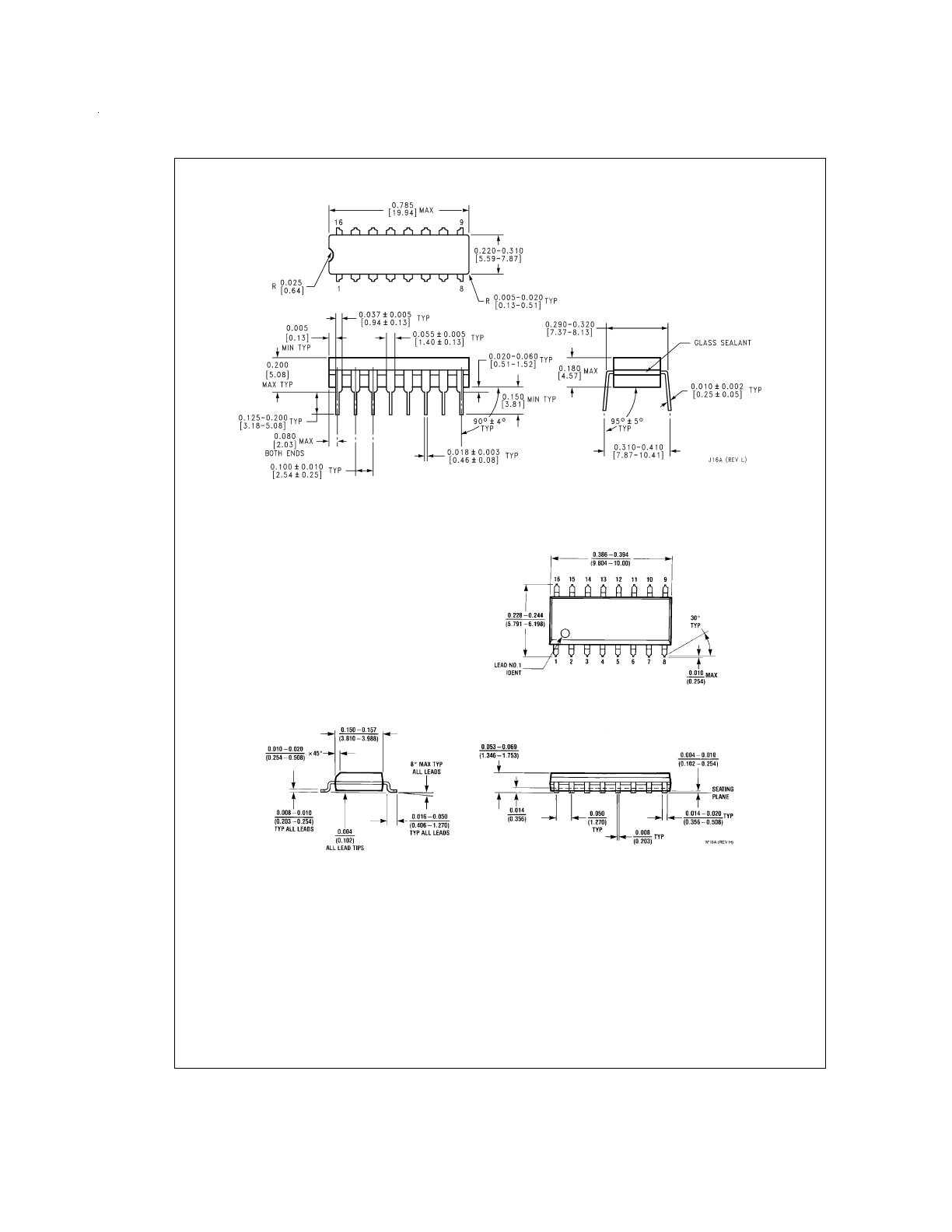
Dual-In-Line Package
DS005255-2
Top View
Order Number DS26LS32CM, DS26LS32CN,
DS26LS32ACM, DS26LS32ACN, DS26LS33ACM
or DS26LS33ACN
See NS Package Number M16A or N16E
For Complete Military Product Specifications,
refer to the appropriate SMD or MDS.
Order Number DS26LS32MJ/883, DS26LS32MW/883,
DS26LS32ME/883, DS26LS33MW/883
See NS Package Number E20A, J16A or W16A
20-Lead Ceramic Leadless Chip Carrier
DS005255-12
www.national.com
2
Absolute Maximum Ratings
(Note 3)
If Military/Aerospace specified devices are required,
please contact the National Semiconductor Sales Office/
Distributors for availability and specifications.
Supply Voltage
7V
Common-Mode Range
±
25V
Differential Input Voltage
±
25V
Enable Voltage
7V
Output Sink Current
50 mA
Maximum Power Dissipation (Note 1) at 25˚C
Cavity Package
1433 mW
Molded Dip Package
1362 mW
SO Package DS26LS32
1002 mW
DS26LS32A
1051 mW
Storage Temperature Range
−65˚C to
+165˚C
Lead Temperature (Soldering, 4 seconds)
260˚C
Operating Conditions
Min
Max
Units
Supply Voltage, (V
CC
)
DS26LS32M, DS26LS33M
4.5
5.5
V
(MIL)
DS26LS32C, DS26LS33C
4.75
5.25
V
DS26LS32AC, DS26LS33AC
(COML)
Temperature, (T
A
)
DS26LS32M, DS26LS33M
−55
+125
˚C
(MIL)
DS26LS32C, DS26LS33C
0
+70
˚C
DS26LS32AC, DS26LS33AC
(COML)
Note 1: Derate cavity package 9.6 mW/˚C above 25˚C; derate molded DIP
package 10.9 mW/˚C above 25˚C.
Note 2: Derate SO Package 8.01 mW/˚C for DS26LS32
8.41 mW/˚C for DS26LS32A
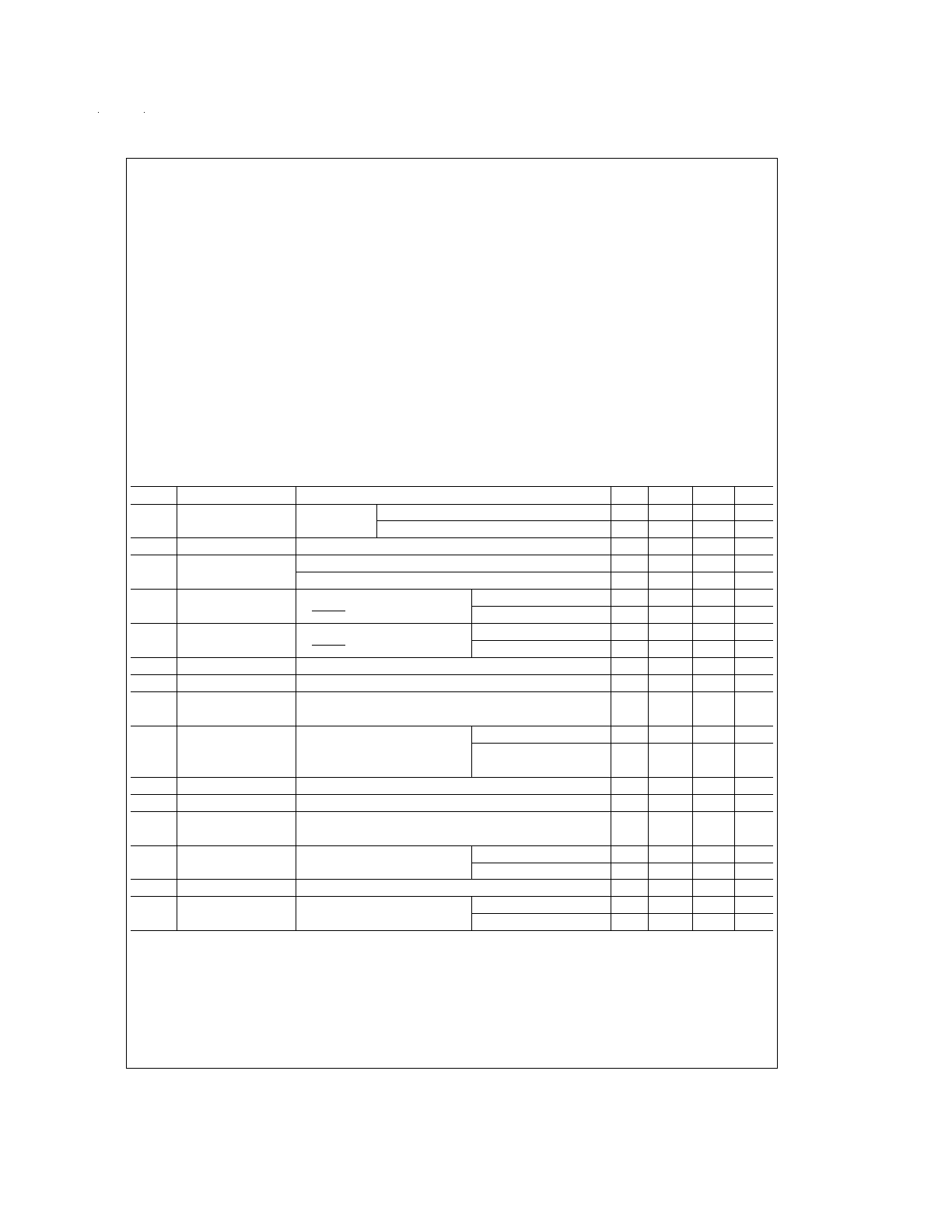
Electrical Characteristics
(Notes 4, 5, 6)
over the operating temperature range unless otherwise specified
Symbol
Parameter
Conditions
Min
Typ
Max
Units
V
TH
Differential Input
V
OUT
= V
OH
DS26LS32, DS26LS32A, −7V
≤
V
CM
≤
+7V
−0.2
±
0.07
0.2
V
Voltage
or V
OL
DS26LS33, DS26LS33A, −15V
≤
V
CM
+15V
−0.5
±
0.14
0.5
V
R
IN
Input Resistance
−15V
≤
V
CM
≤
+15V (One Input AC GND)
6.0
8.5
k
Ω
I
IN
Input Current (Under
V
IN
= 15V, Other Input −15V
≤
V
IN
≤
+15V
2.3
mA
Test)
V
IN
= −15V, Other Input −15V
≤
V
IN
≤
+15V
−2.8
mA
V
OH
Output High Voltage
V
CC
= MIN,
∆
V
IN
= 1V,
Commercial
2.7
4.2
V
V
ENABLE
= 0.8V, I
OH
= −440 µA
Military
2.5
4.2
V
V
OL
Output Low Voltage
V
CC
= Min,
∆
V
IN
= −1V,
I
OL
= 4 mA
0.4
V
V
ENABLE
= 0.8V
I
OL
= 8 mA
0.45
V
V
IL
Enable Low Voltage
0.8
V
V
IH
Enable High Voltage
2.0
V
V
I
Enable Clamp
V
CC
= Min, I
IN
= −18 mA
−1.5
V
Voltage
I
O
OFF-State (High
V
CC
= Max
V
O
= 2.4V
20
µA
Impedance) Output
V
O
= 0.4V
−20
µA
Current
I
IL
Enable Low Current
V
IN
= 0.4V
−0.36
mA
I
IH
Enable High Current
V
IN
= 2.7V
20
µA
I
SC
Output Short-Circuit
V
O
= 0V, V
CC
= Max,
∆
V
IN
= 1V
−15
−85
mA
Current
I
CC
Power Supply
V
CC
= Max, All V
IN
= GND,
DS26LS32, DS26LS32A
52
70
mA
Current
Outputs Disabled
DS26LS33, DS26LS33A
57
80
mA
I
I
Input High Current
V
IN
= 5.5V
100
µA
V
HYST
Input Hysteresis
T
A
= 25˚C, V
CC
= 5V,
DS26LS32, DS26S32A
100
mV
V
CM
= 0V
DS26LS33, DS26LS33A
200
mV
Note 3: “Absolute Maximum Ratings” are those values beyond which the safety of the device cannot be guaranteed. They are not meant to imply that the device
should be operated at these limits. The table of “Electrical Characteristics” provides conditions for actual device operation.
Note 4: All currents into device pins are shown as positive, all currents out of device pins are shown as negative, all voltages are referenced to ground, unless oth-
erwise specified. All values shown as max or min are so classified on absolute value basis.
Note 5: All typical values are V
CC
= 5V, T
A
= 25˚C.
Note 6: Only one output at a time should be shorted.
www.national.com
3
Switching Characteristics
V
CC
= 5V, T
A
= 25˚C
Symbol
Parameter
Conditions
DS26LS32/DS26LS33
DS26LS32A/DS26LS33A
Units
Min
Typ
Max
Min
Typ
Max
t
PLH
Input to Output
C
L
= 15 pF
17
25
23
35
ns
t
PHL
17
25
23
35
ns
t
LZ
ENABLE to Output
C
L
= 5 pF
20
30
15
30
ns
t
HZ
15
22
20
25
ns
t
ZL
ENABLE to Output
C
L
= 15 pF
15
22
14
22
ns
t
ZH
15
22
15
22
ns
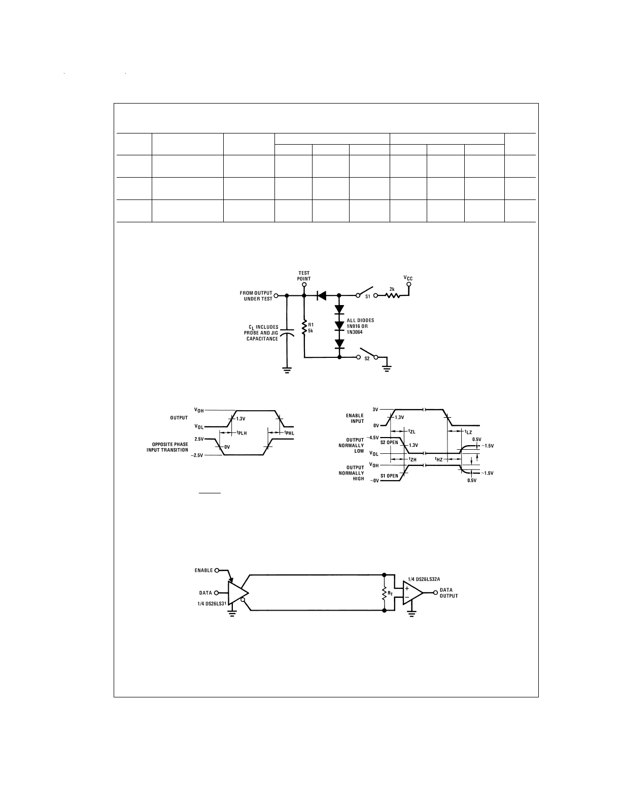
AC Test Circuit and Switching Time Waveforms
Typical Applications
Load Test Circuit for TRI-STATE
®
Outputs
DS005255-3
Propagation Delay (Notes 7, 9)
DS005255-4
Enable and Disable Times (Notes 8, 9)
DS005255-5
Note 7: Diagram shown for ENABLE low.
Note 8: S1 and S2 of load circuit are closed except where shown.
Note 9: Pulse generator for all pulses: Rate = 1.0 MHz; Z
O
= 50
Ω
; t
r
≤
6 ns; t
f
≤
6.0 ns.
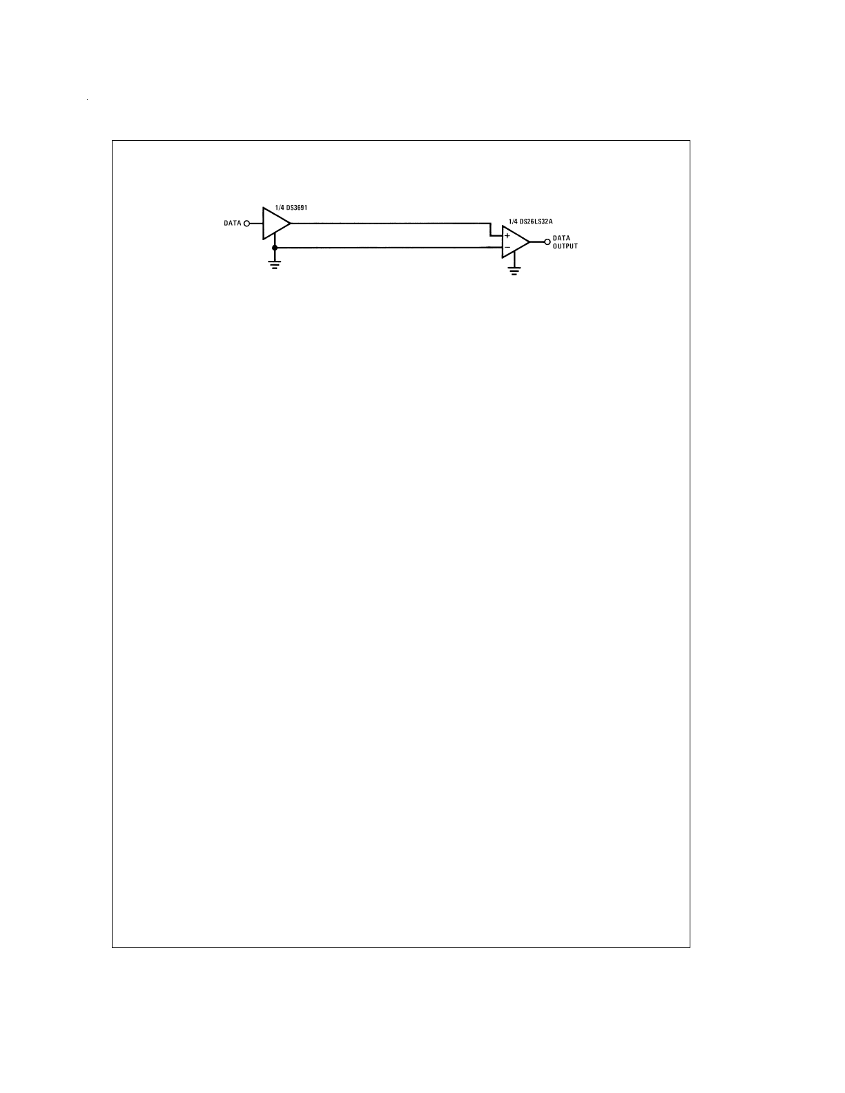
Two-Wire Balanced Interface — RS-422
DS005255-6
www.national.com
4
Typical Applications
(Continued)
Single Wire with Driver Ground Reference — RS-423
DS005255-7
www.national.com
5
Physical Dimensions
inches (millimeters) unless otherwise noted
Ceramic Dual-In-Line Package (J)
Order Number DS26LS32MJ/883 or DS26LS33MJ/883
NS Package Number J16A
Small Outline Package (M)
Order Number DS26LS32CM, DS26LS32ACM, or DS26LS33ACM
NS Package Number M16A
www.national.com
6
Physical Dimensions
inches (millimeters) unless otherwise noted (Continued)
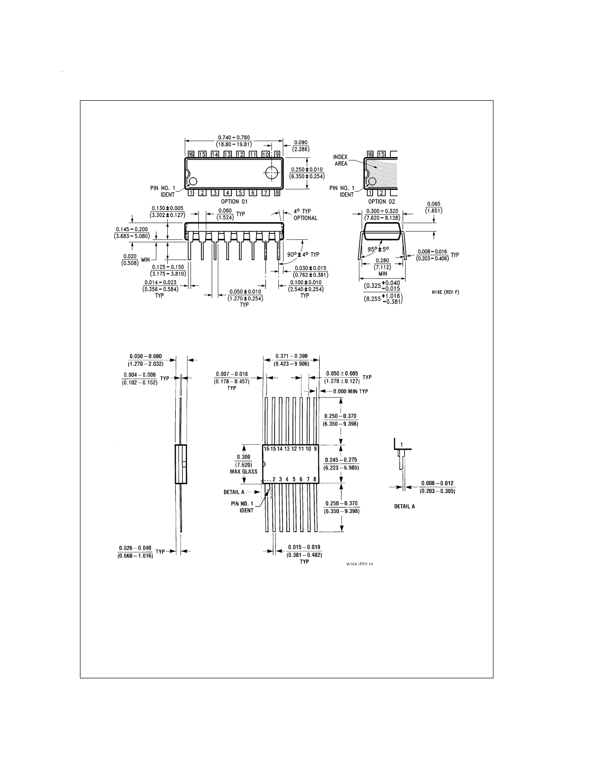
Molded Dual-In-Line Package (N)
Order Number DS26LS32CN, DS26LS32ACN, or DS26LS33ACN
NS Package Number N16E
16 Lead Ceramic Flatpak (W)
Order Number DS26LS32MW/883 or DS26LS33MW/883
NS Package Number W16A
www.national.com
7
Physical Dimensions
inches (millimeters) unless otherwise noted (Continued)
LIFE SUPPORT POLICY
NATIONAL’S PRODUCTS ARE NOT AUTHORIZED FOR USE AS CRITICAL COMPONENTS IN LIFE SUPPORT DE-
VICES OR SYSTEMS WITHOUT THE EXPRESS WRITTEN APPROVAL OF THE PRESIDENT OF NATIONAL SEMI-
CONDUCTOR CORPORATION. As used herein:
1. Life support devices or systems are devices or sys-
tems which, (a) are intended for surgical implant into
the body, or (b) support or sustain life, and whose fail-
ure to perform when properly used in accordance
with instructions for use provided in the labeling, can
be reasonably expected to result in a significant injury
to the user.
2. A critical component in any component of a life support
device or system whose failure to perform can be rea-
sonably expected to cause the failure of the life support
device or system, or to affect its safety or effectiveness.
National Semiconductor
Corporation
Americas
Tel: 1-800-272-9959
Fax: 1-800-737-7018
Email: support@nsc.com
www.national.com
National Semiconductor
Europe
Fax: +49 (0) 1 80-530 85 86
Email: europe.support@nsc.com
Deutsch Tel: +49 (0) 1 80-530 85 85
English
Tel: +49 (0) 1 80-532 78 32
Français Tel: +49 (0) 1 80-532 93 58
Italiano
Tel: +49 (0) 1 80-534 16 80
National Semiconductor
Asia Pacific Customer
Response Group
Tel: 65-2544466
Fax: 65-2504466
Email: sea.support@nsc.com
National Semiconductor
Japan Ltd.
Tel: 81-3-5639-7560
Fax: 81-3-5639-7507
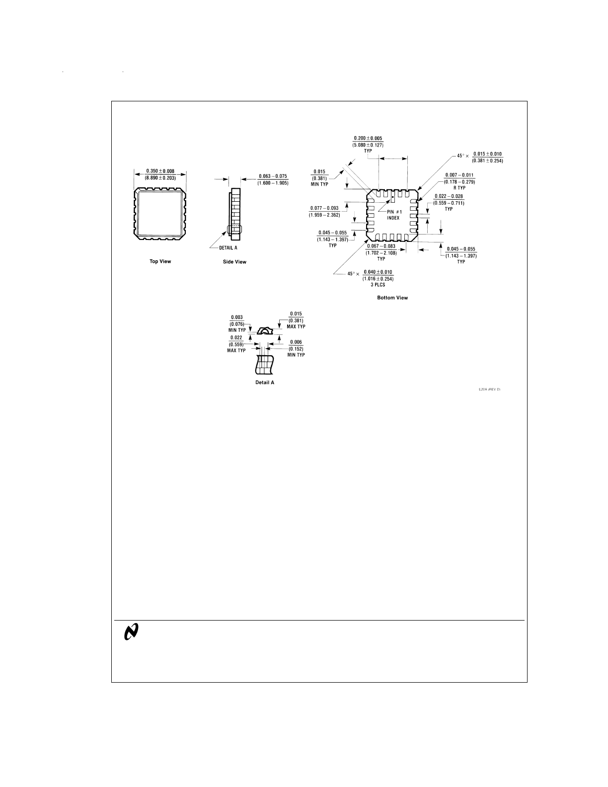
20 Lead Ceramic Leadless Chip Carrier (E)
Order Number DS26LS32ME/883
NS Package Number E20A
DS26LS32C/DS26LS32M/DS26LS32AC/DS26LS33C/DS26LS33M/DS26LS33AC
Quad
Differential
Line
Receivers
National does not assume any responsibility for use of any circuitry described, no circuit patent licenses are implied and National reserves the right at any time without notice to change said circuitry and specifications.