
DS1489/DS1489A
Quad Line Receiver
General Description
The DS1489/DS1489A are quad line receivers designed to
interface data terminal equipment with data communications
equipment. They are constructed on a single monolithic sili-
con chip. These devices satisfy the specifications of EIA
Standard RS-232D. The DS1489/DS1489A meet and ex-
ceed the specifications of MC1489/MC1489A and are
pin-for-pin replacements.
Features
n
Four separate receivers per package
n
Programmable threshold
n
Built-in input threshold hysteresis
n
“Fail safe” operating mode: high output for open inputs
n
Inputs withstand
±
30V
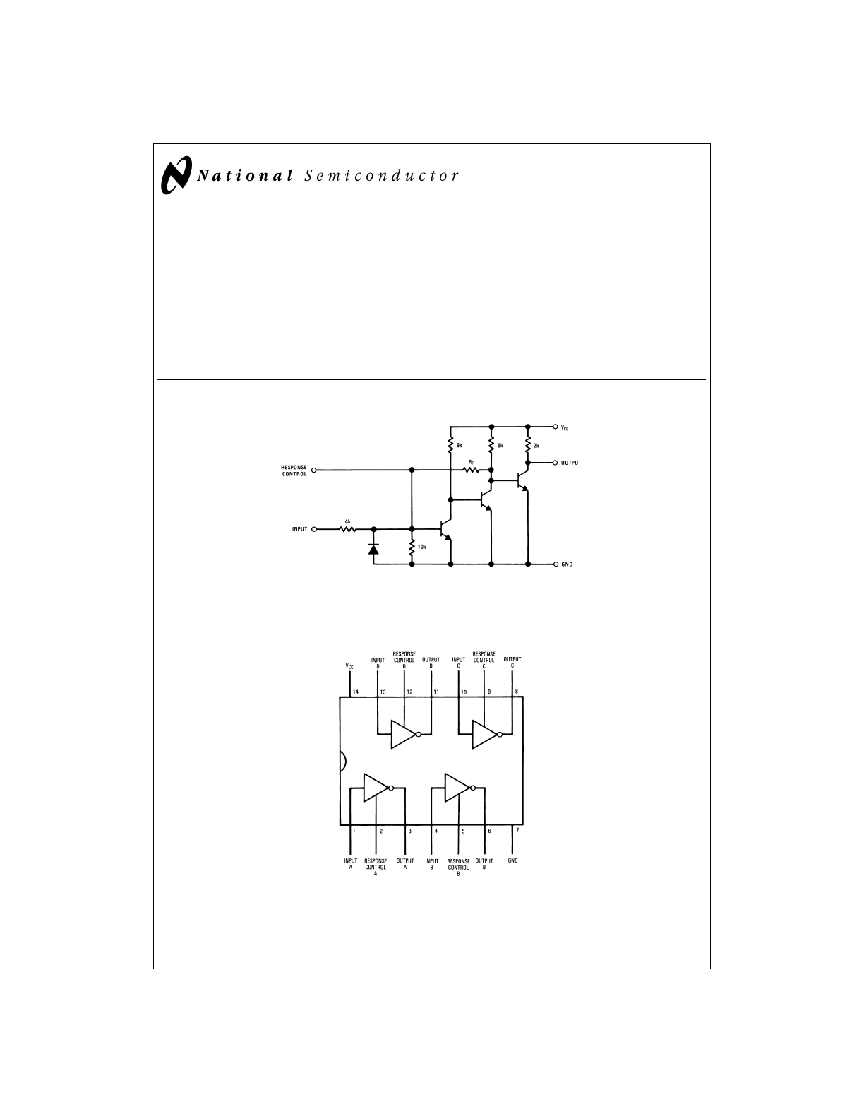
Schematic and Connection Diagrams
DS005777-1
(
1
⁄
4
of unit shown)
DS1489: R
F
= 10k
DS1489A: R
F
= 2k
Dual-In-Line Package
DS005777-2
Top View
Order Number DS1489M, DS1489N
DS1489AM or DS1489AN
See NS Package Number M14A or N14A
May 1998
DS1489/DS1489A
Quad
Line
Receiver
© 1998 National Semiconductor Corporation
DS005777
www.national.com
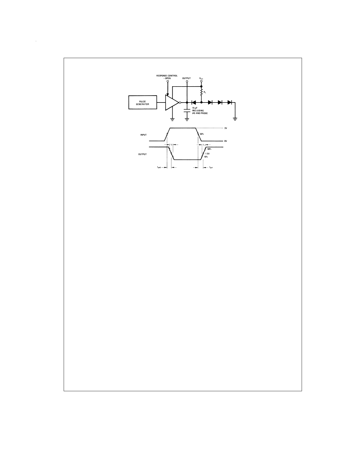
AC Test Circuit and Voltage Waveforms
DS005777-3
DS005777-4
FIGURE 1.
www.national.com
2
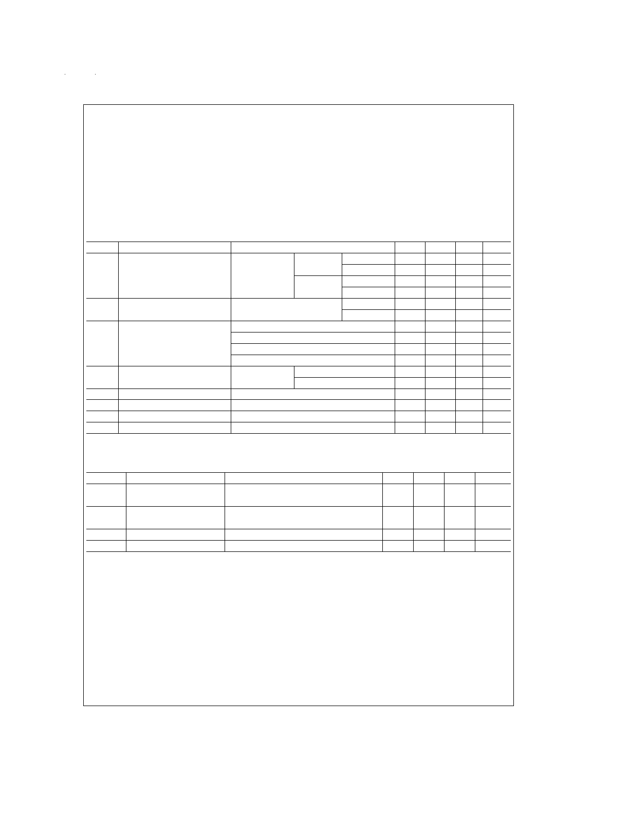
Absolute Maximum Ratings
(Note 2)
If Military/Aerospace specified devices are required,
please contact the National Semiconductor Sales Office/
Distributors for availability and specifications.
Power Supply Voltage
10V
Input Voltage Range
±
30V
Output Load Current
20 mA
Power Dissipation (Note 3)
1W
Operating Temperature Range
0˚C to +75˚C
Storage Temperature Range
−65˚C to +150˚C
Maximum Power Dissipation (Note 1) at 25˚C
Molded DIP Package
1207 mW
SO Package
1042 mW
Lead Temperature (Soldering, 4
sec.)
260˚C
Note 1: Derate molded DIP package 9.7 mW/˚C above 25˚C; derate SO
package 8.33 mW/˚C above 25˚C.
Electrical Characteristics
(Notes 3, 4, 5)
DS1489/DS1489A: The following apply for V
CC
= 5.0V
±
1%, 0˚C
≤
T
A
≤
+75˚C unless otherwise specified.
Symbol
Parameter
Conditions
Min
Typ
Max
Units
V
TH
Input High Threshold Voltage
V
OUT
≤
0.45V,
DS1489
T
A
= 25˚C
1.0
1.25
1.5
V
I
OUT
= 10 mA
0.9
1.6
V
DS1489A
T
A
= 25˚C
1.75
2.00
2.25
V
1.55
2.40
V
V
TL
Input Low Threshold Voltage
V
OUT
≥
2.5V,
T
A
= 25˚C
0.75
1.00
1.25
V
I
OUT
= −0.5 mA
0.65
1.35
V
I
IN
Input Current
V
IN
= +25V
+3.6
+5.6
+8.3
mA
V
IN
= −25V
−3.6
−5.6
−8.3
mA
V
IN
= +3V
+0.43
+0.53
mA
V
IN
= −3V
−0.43
−0.53
mA
V
OH
Output High Voltage
I
OUT
= −0.5 mA
V
IN
= 0.75V
2.6
3.8
5.0
V
Input = Open
2.6
3.8
5.0
V
V
OL
Output Low Voltage
V
IN
= 3.0V, I
OUT
= 10 mA
0.33
0.45
V
I
SC
Output Short Circuit Current
V
IN
= 0.75V
−3.0
mA
I
CC
Supply Current
V
IN
= 5.0V
14
26
mA
P
d
Power Dissipation
V
IN
= 5.0V
70
130
mW
Switching Characteristics
V
CC
= 5V, T
A
= 25˚C
Symbol
Parameter
Conditions
Min
Typ
Max
Units
t
pd1
Input to Output “High”
R
L
= 3.9k, (
Figure 1
) (AC Test Circuit)
28
85
ns
Propagation Delay
t
pd0
Input to Output “Low”
R
L
= 390
Ω
, (
Figure 1
) (AC Test Circuit)
20
50
ns
Propagation Delay
t
r
Output Rise Time
R
L
= 3.9k, (
Figure 1
) (AC Test Circuit)
110
175
ns
t
f
Output Fall Time
R
L
= 390
Ω
, (
Figure 1
) (AC Test Circuit)
9
20
ns
Note 2: “Absolute Maximum Ratings” are those values beyond which the safety of the device cannot be guaranteed. Except for “Operating Temperature Range” they
are not meant to imply that the devices should be operated at these limits. The table of “Electrical Characteristics” provides conditions for actual device operation.
Note 3: Unless otherwise specified min/max limits apply across the 0˚C to +75˚C temperature range for the DS1489 and DS1489A.
Note 4: All currents into device pins shown as positive, out of device pins as negative, all voltages referenced to ground unless otherwise noted. All values shown
as max or min on absolute value basis.
Note 5: These specifications apply for response control pin = open.
www.national.com
3

Typical Characteristics
V
CC
= 5.0V, T
A
= +25˚C unless otherwise noted
DS005777-7
FIGURE 2. Input Current
DS005777-8
FIGURE 3. DS1489 Input Threshold Voltage Adjustment
DS005777-9
FIGURE 4. DS1489A Input Threshold Voltage
Adjustment
DS005777-10
FIGURE 5. Input Threshold Voltage vs Temperature
DS005777-11
FIGURE 6. Input Threshold vs Power Supply Voltage
DS005777-12
FIGURE 7. Noise Rejection vs Capacitance for
DS1489A
www.national.com
4
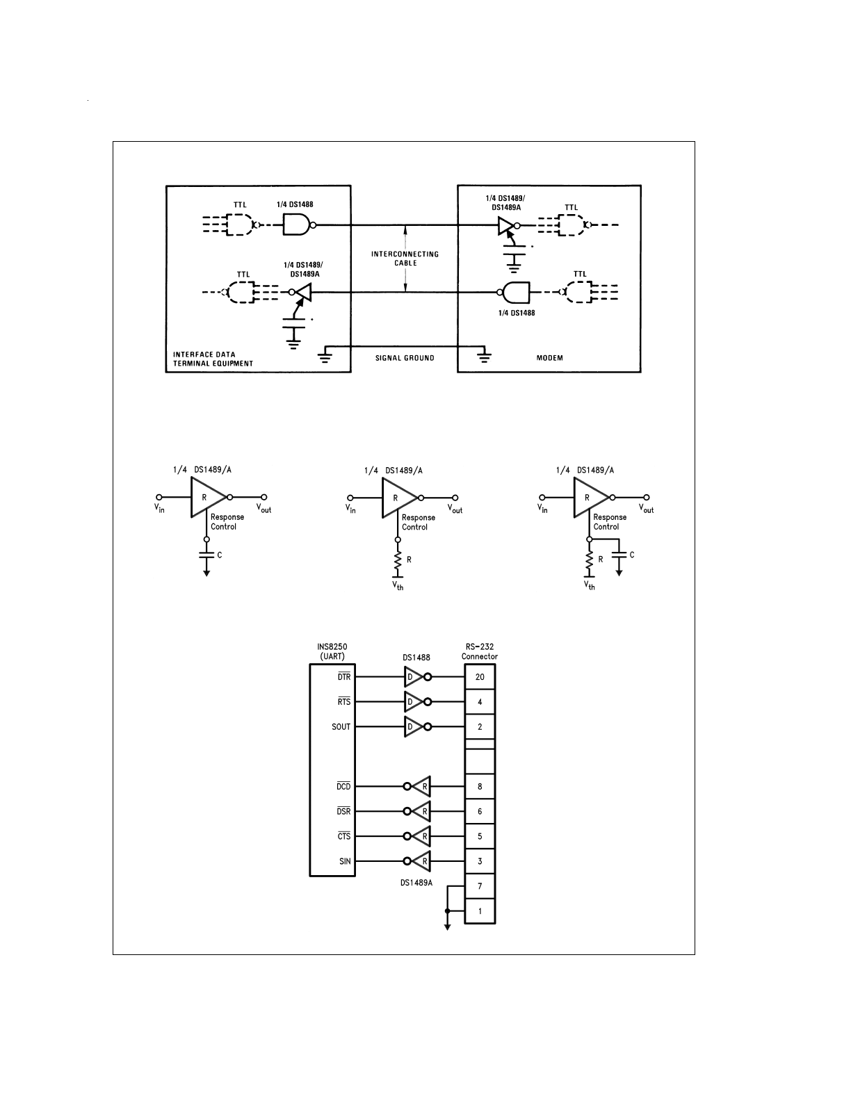
Typical Application Information
DS005777-5
*Optional for noise filtering.
Applications Using the Response Control Pin
Noise Filter
See
Figure 7
DS005777-13
Threshold Shift
See
Figures 3, 4
DS005777-14
Noise Filter and Threshold Shift
See
Figures 3, 4, 7
DS005777-15
Application of DS1488, DS1489A and INS8250
DS005777-16
www.national.com
5

6
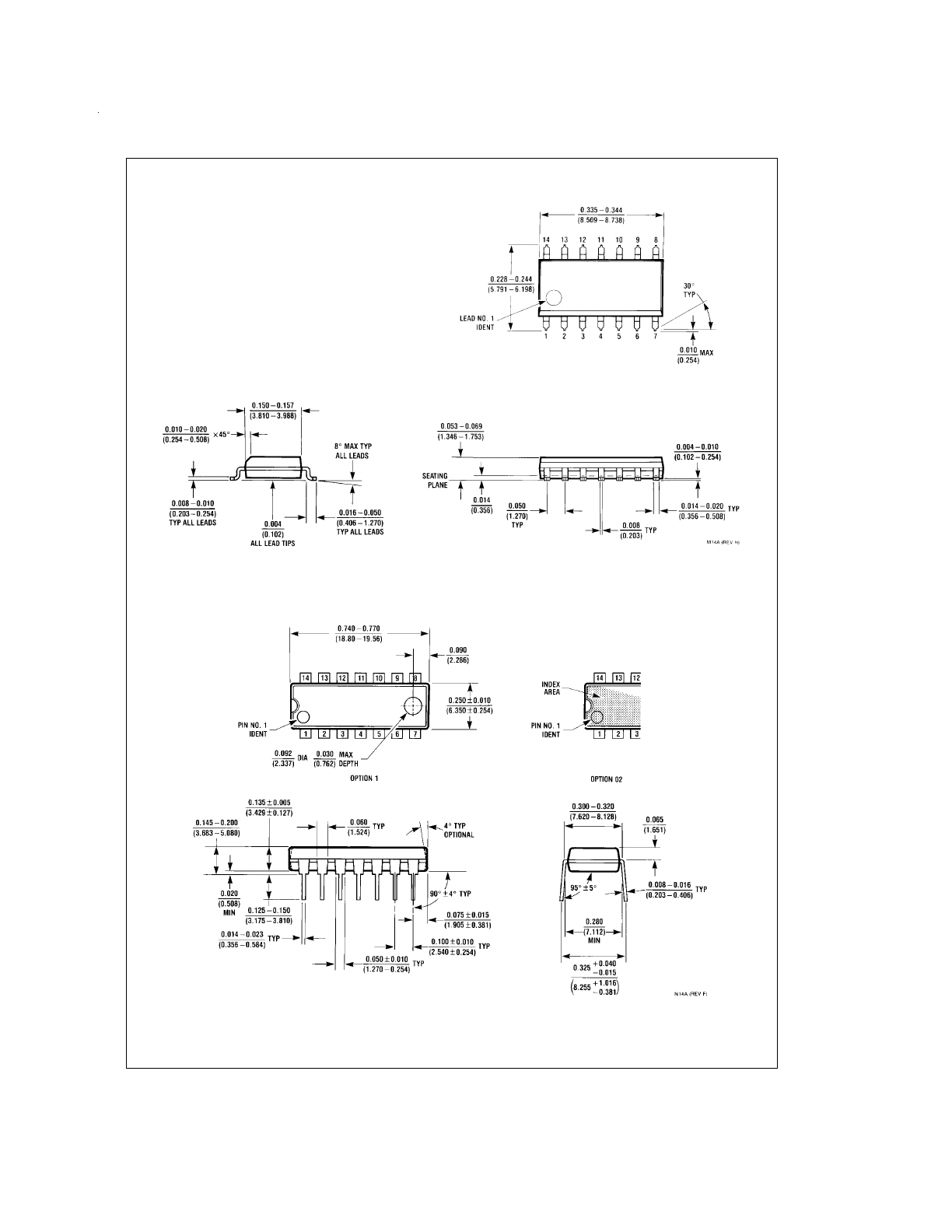
Physical Dimensions
inches (millimeters) unless otherwise noted
SO Package (M)
Order Number DS1489M or DS1489AM
NS Package Number M14A
Molded Dual-In-Line Package (N)
Order Number DS1489N or DS1489AN
NS Package Number N14A
www.national.com
7

LIFE SUPPORT POLICY
NATIONAL’S PRODUCTS ARE NOT AUTHORIZED FOR USE AS CRITICAL COMPONENTS IN LIFE SUPPORT DE-
VICES OR SYSTEMS WITHOUT THE EXPRESS WRITTEN APPROVAL OF THE PRESIDENT OF NATIONAL SEMI-
CONDUCTOR CORPORATION. As used herein:
1. Life support devices or systems are devices or sys-
tems which, (a) are intended for surgical implant into
the body, or (b) support or sustain life, and whose fail-
ure to perform when properly used in accordance
with instructions for use provided in the labeling, can
be reasonably expected to result in a significant injury
to the user.
2. A critical component in any component of a life support
device or system whose failure to perform can be rea-
sonably expected to cause the failure of the life support
device or system, or to affect its safety or effectiveness.
National Semiconductor
Corporation
Americas
Tel: 1-800-272-9959
Fax: 1-800-737-7018
Email: support@nsc.com
www.national.com
National Semiconductor
Europe
Fax: +49 (0) 1 80-530 85 86
Email: europe.support@nsc.com
Deutsch Tel: +49 (0) 1 80-530 85 85
English
Tel: +49 (0) 1 80-532 78 32
Français Tel: +49 (0) 1 80-532 93 58
Italiano
Tel: +49 (0) 1 80-534 16 80
National Semiconductor
Asia Pacific Customer
Response Group
Tel: 65-2544466
Fax: 65-2504466
Email: sea.support@nsc.com
National Semiconductor
Japan Ltd.
Tel: 81-3-5620-6175
Fax: 81-3-5620-6179
DS1489/DS1489A
Quad
Line
Receiver
National does not assume any responsibility for use of any circuitry described, no circuit patent licenses are implied and National reserves the right at any time without notice to change said circuitry and specifications.