
LM2940/LM2940C
1A Low Dropout Regulator
General Description
The LM2940/LM2940C positive voltage regulator features
the ability to source 1A of output current with a dropout volt-
age of typically 0.5V and a maximum of 1V over the entire
temperature range. Furthermore, a quiescent current reduc-
tion circuit has been included which reduces the ground cur-
rent when the differential between the input voltage and the
output voltage exceeds approximately 3V. The quiescent
current with 1A of output current and an input-output differ-
ential of 5V is therefore only 30 mA. Higher quiescent cur-
rents only exist when the regulator is in the dropout mode
(V
IN
− V
OUT
≤
3V).
Designed also for vehicular applications, the LM2940/
LM2940C and all regulated circuitry are protected from re-
verse battery installations or 2-battery jumps. During line
transients, such as load dump when the input voltage can
momentarily exceed the specified maximum operating volt-
age, the regulator will automatically shut down to protect
both the internal circuits and the load. The LM2940/
LM2940C cannot be harmed by temporary mirror-image in-
sertion. Familiar regulator features such as short circuit and
thermal overload protection are also provided.
Features
n
Dropout voltage typically 0.5V
@
I
O
= 1A
n
Output current in excess of 1A
n
Output voltage trimmed before assembly
n
Reverse battery protection
n
Internal short circuit current limit
n
Mirror image insertion protection
n
P
+
Product Enhancement tested
Typical Application
Ordering Information
Temperature
Range
Output Voltage
Package
5.0
8.0
9.0
10
12
15
0˚C
≤
T
J
≤
125˚C
LM2940CT-5.0
LM2940CT-9.0
LM2940CT-12
LM2940CT-15
TO-220
LM2940CS-5.0
LM2940CS-9.0
LM2940CS-12
LM2940CS-15
TO-263
−40˚C
≤
T
J
≤
125˚C
LM2940T-5.0
LM2940T-8.0
LM2940T-9.0
LM2940T-10
LM2940T-12
TO-220
LM2940S-5.0
LM2940S-8.0
LM2940S-9.0
LM2940S-10
LM2940S-12
TO-263
−40˚C
≤
T
J
≤
85˚C
LM2940IMP-5.0
LM2940IMP-8.0
LM2940IMP-9.0
LM2940IMP-10
LM2940IMP-12
LM2940IMP-15
SOT-223
LM2940IMPX-5.0 LM2940IMPX-8.0 LM2940IMPX-9.0 LM2940IMPX-10 LM2940IMPX-12 LM2940IMPX-15 SOT-223
in Tape
and Reel
SOT-223 Package
Marking
L53B
L54B
L0EB
L55B
L56B
L70B
The physical size of the SOT-223 is too small to contain the full device part number. The package markings indicated are what will appear on the actual device.
Temperature
Range
Output Voltage
Package
5.0
8.0
12
15
−55˚C
≤
T
J
≤
125˚C
LM2940J-5.0/883
5962-8958701EA
LM2940J-8.0/883
5962-9088301QEA
LM2940J-12/883
5962-9088401QEA
LM2940J-15/883
5962-9088501QEA
J16A
LM2940WG5.0/883
5962-8958701XA
WG16A
For information on military temperature range products, please go to the Mil/Aero Web Site at http://www.national.com/appinfo/milaero/index.html.
DS008822-3
*
Required if regulator is located far from power supply filter.
**
C
OUT
must be at least 22 µF to maintain stability. May be increased without bound to maintain regulation during transients. Locate as close as possible
to the regulator. This capacitor must be rated over the same operating temperature range as the regulator and the ESR is critical; see curve.
July 2000
LM2940/LM2940C
1A
Low
Dropout
Regulator
© 2000 National Semiconductor Corporation
DS008822
www.national.com
Connection Diagrams
(TO-220) Plastic Package
DS008822-2
Front View
Order Number LM2940CT-5.0, LM2940CT-9.0,
LM2940CT-12, LM2940CT-15, LM2940T-5.0,
LM2940T-8.0, LM2940T-9.0,
LM2940T-10 or LM2940T-12
See NS Package Number TO3B
3-Lead SOT-223
DS008822-42
Front View
Order Part Number LM2940IMP-5.0,
LM2940IMP-8.0, LM2940IMP-9.0,
LM2940IMP-10, LM2940IMP-12 or LM2940IMP-15
See NS Package Number MP04A
16-Lead Dual-in-Line Package (J)
DS008822-43
Top View
Order Number LM2940J-5.0/883 (5962-8958701EA),
LM2940J-8.0/883 (5962-9088301QEA),
LM2940J-12/883 (5962-9088401QEA),
LM2940J-15/883 (5962-9088501QEA)
See NS Package Number J16A
16-Lead Ceramic Surface-Mount Package (WG)
DS008822-44
Top View
Order Number LM2940WG5.0/883 (5962-8958701XA)
See NS Package Number WG16A
(TO-263) Surface-Mount Package
DS008822-11
Top View
DS008822-12
Side View
Order Number LM2940CS-5.0, LM2940CS-9.0,
LM2940CS-12, LM2940CS-15,
LM2940S-5.0, LM2940S-8.0,
LM2940S-9.0, LM2940S-10 or LM2940S-12
See NS Package Number TS3B
LM2940/LM2940C
www.national.com
2
Absolute Maximum Ratings
(Note 1)
If Military/Aerospace specified devices are required,
please contact the National Semiconductor Sales Office/
Distributors for availability and specifications.
LM2940S, T, MP
≤
100 ms
60V
LM2940CS, T
≤
1 ms
45V
Internal Power Dissipation
(Note 2)
Internally Limited
Maximum Junction Temperature
150˚C
Storage Temperature Range
−65˚C
≤
T
J
≤
+150˚C
Lead Temperature, Time for Wave Soldering
TO-220 (T) Package
260˚C, 10s
TO-263 (S) Package
260˚C, 4s
SOT-223 (MP) Package
260˚C, 4s
ESD Susceptibility (Note 3)
2 kV
Operating Conditions
(Note 1)
Input Voltage
26V
Temperature Range
LM2940T, LM2940S
−40˚C
≤
T
J
≤
125˚C
LM2940CT, LM2940CS
0˚C
≤
T
J
≤
125˚C
LM2940IMP
−40˚C
≤
T
J
≤
85˚C
LM2940J, LM2940WG
−55˚C
≤
T
J
≤
125˚C
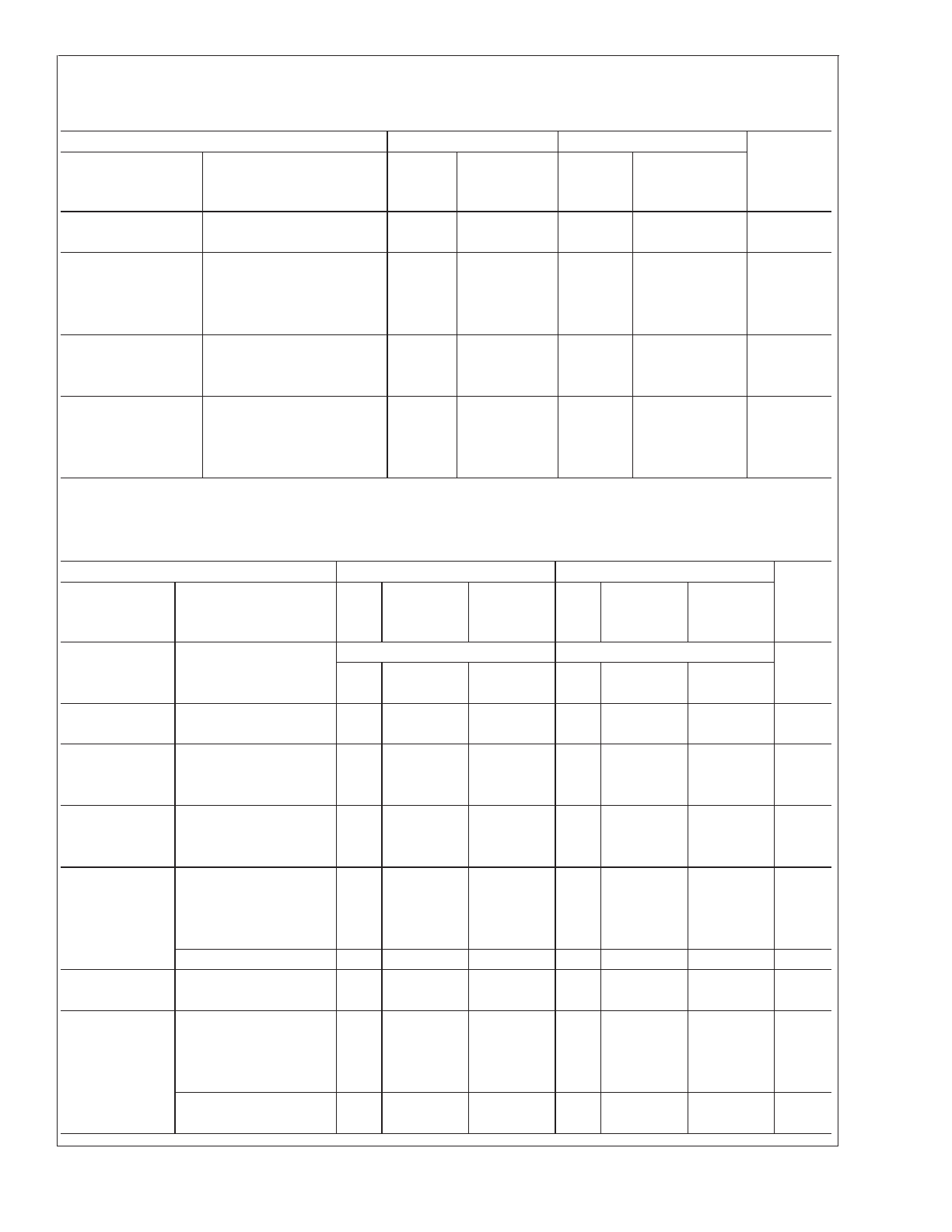
Electrical Characteristics
V
IN
= V
O
+ 5V, I
O
= 1A, C
O
= 22 µF, unless otherwise specified. Boldface limits apply over the entire operating tempera-
ture range of the indicated device. All other specifications apply for T
A
= T
J
= 25˚C.
Output Voltage (V
O
)
5V
8V
Units
LM2940
LM2940/883
LM2940
LM2940/883
Parameter
Conditions
Typ
Limit
Limit
Typ
Limit
Limit
(Note 4)
(Note 5)
(Note 4)
(Note 5)
6.25V
≤
V
IN
≤
26V
9.4V
≤
V
IN
≤
26V
Output Voltage
5 mA
≤
I
O
≤
1A
5.00
4.85/4.75
4.85/4.75
8.00
7.76/7.60
7.76/7.60
V
MIN
5.15/5.25
5.15/5.25
8.24/8.40
8.24/8.40
V
MAX
Line Regulation
V
O
+ 2V
≤
V
IN
≤
26V,
20
50
40/50
20
80
50/80
mV
MAX
I
O
= 5 mA
Load Regulation
50 mA
≤
I
O
≤
1A
LM2940, LM2940/883
35
50/80
50/100
55
80/130
80/130
mV
MAX
LM2940C
35
50
55
80
Output
100 mADC and
Impedance
20 mArms,
35
1000/1000
55
1000/1000
m
Ω
f
O
= 120 Hz
Quiescent
V
O
+2V
≤
V
IN
≤
26V,
Current
I
O
= 5 mA
LM2940, LM2940/883
10
15/20
15/20
10
15/20
15/20
mA
MAX
LM2940C
10
15
V
IN
= V
O
+ 5V,
30
45/60
50/60
30
45/60
50/60
mA
MAX
I
O
= 1A
Output Noise
10 Hz − 100 kHz,
150
700/700
240
1000/1000
µV
rms
Voltage
I
O
= 5 mA
Ripple Rejection
f
O
= 120 Hz, 1 V
rms
,
I
O
= 100 mA
LM2940
72
60/54
66
54/48
dB
MIN
LM2940C
72
60
66
54
f
O
= 1 kHz, 1 V
rms
,
60/50
54/48
dB
MIN
I
O
= 5 mA
Long Term
20
32
mV/
Stability
1000 Hr
Dropout Voltage
I
O
= 1A
0.5
0.8/1.0
0.7/1.0
0.5
0.8/1.0
0.7/1.0
V
MAX
I
O
= 100 mA
110
150/200
150/200
110
150/200
150/200
mV
MAX
Short Circuit
Current
(Note 6)
1.9
1.6
1.5/1.3
1.9
1.6
1.6/1.3
A
MIN
LM2940/LM2940C
www.national.com
3
Electrical Characteristics
(Continued)
V
IN
= V
O
+ 5V, I
O
= 1A, C
O
= 22 µF, unless otherwise specified. Boldface limits apply over the entire operating tempera-
ture range of the indicated device. All other specifications apply for T
A
= T
J
= 25˚C.
Output Voltage (V
O
)
5V
8V
Units
LM2940
LM2940/883
LM2940
LM2940/883
Parameter
Conditions
Typ
Limit
Limit
Typ
Limit
Limit
(Note 4)
(Note 5)
(Note 4)
(Note 5)
Maximum Line
R
O
= 100
Ω
V
MIN
Transient
LM2940, T
≤
100 ms
75
60/60
75
60/60
LM2940/883, T
≤
20 ms
40/40
40/40
LM2940C, T
≤
1 ms
55
45
55
45
Reverse Polarity
R
O
= 100
Ω
DC Input Voltage
LM2940, LM2940/883
−30
−15/−15
−15/−15
−30
−15/−15
−15/−15
V
MIN
LM2940C
−30
−15
−30
−15
Reverse Polarity
R
O
= 100
Ω
Transient Input
LM2940, T
≤
100 ms
−75
−50/−50
−75
−50/−50
V
MIN
Voltage
LM2940/883, T
≤
20 ms
−45/−45
−45/−45
LM2940C, T
≤
1 ms
−55
−45/−45
Electrical Characteristics
V
IN
= V
O
+ 5V, I
O
= 1A, C
O
= 22 µF, unless otherwise specified. Boldface limits apply over the entire operating tempera-
ture range of the indicated device. All other specifications apply for T
A
= T
J
= 25˚C.
Output Voltage (V
O
)
9V
10V
Units
Parameter
Conditions
Typ
LM2940
Typ
LM2940
Limit
Limit
(Note 4)
(Note 4)
10.5V
≤
V
IN
≤
26V
11.5V
≤
V
IN
≤
26V
Output Voltage
5 mA
≤
I
O
≤
1A
9.00
8.73/8.55
10.00
9.70/9.50
V
MIN
9.27/9.45
10.30/10.50
V
MAX
Line Regulation
V
O
+ 2V
≤
V
IN
≤
26V,
20
90
20
100
mV
MAX
I
O
= 5 mA
Load Regulation
50 mA
≤
I
O
≤
1A
LM2940
60
90/150
65
100/165
mV
MAX
LM2940C
60
90
Output Impedance
100 mADC and
20 mArms,
60
65
m
Ω
f
O
= 120 Hz
Quiescent
V
O
+2V
≤
V
IN
<
26V,
Current
I
O
= 5 mA
LM2940
10
15/20
10
15/20
mA
MAX
LM2940C
10
15
V
IN
= V
O
+ 5V, I
O
= 1A
30
45/60
30
45/60
mA
MAX
Output Noise
10 Hz − 100 kHz,
270
300
µV
rms
Voltage
I
O
= 5 mA
Ripple Rejection
f
O
= 120 Hz, 1 V
rms
,
I
O
= 100 mA
LM2940
64
52/46
63
51/45
dB
MIN
LM2940C
64
52
Long Term
Stability
34
36
mV/
1000 Hr
Dropout Voltage
I
O
= 1A
0.5
0.8/1.0
0.5
0.8/1.0
V
MAX
I
O
= 100 mA
110
150/200
110
150/200
mV
MAX
LM2940/LM2940C
www.national.com
4
Electrical Characteristics
(Continued)
V
IN
= V
O
+ 5V, I
O
= 1A, C
O
= 22 µF, unless otherwise specified. Boldface limits apply over the entire operating tempera-
ture range of the indicated device. All other specifications apply for T
A
= T
J
= 25˚C.
Output Voltage (V
O
)
9V
10V
Units
Parameter
Conditions
Typ
LM2940
Typ
LM2940
Limit
Limit
(Note 4)
(Note 4)
Short Circuit
(Note 6)
1.9
1.6
1.9
1.6
A
MIN
Current
Maximum Line
R
O
= 100
Ω
Transient
T
≤
100 ms
LM2940
75
60/60
75
60/60
V
MIN
LM2940C
55
45
Reverse Polarity
R
O
= 100
Ω
DC Input Voltage
LM2940
−30
−15/−15
−30
−15/−15
V
MIN
LM2940C
−30
−15
Reverse Polarity
R
O
= 100
Ω
Transient Input
T
≤
100 ms
Voltage
LM2940
−75
−50/−50
−75
−50/−50
V
MIN
LM2940C
−55
−45/−45
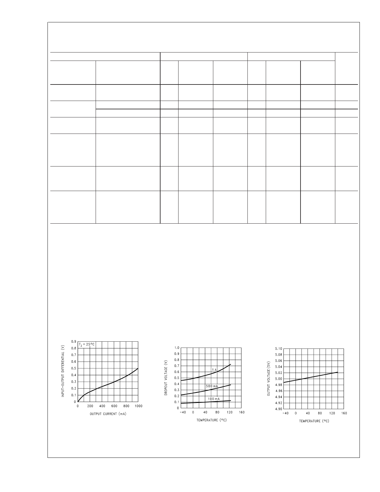
Electrical Characteristics
V
IN
= V
O
+ 5V, I
O
= 1A, C
O
= 22 µF, unless otherwise specified. Boldface limits apply over the entire operating tempera-
ture range of the indicated device. All other specifications apply for T
A
= T
J
= 25˚C.
Output Voltage (V
O
)
12V
15V
Units
LM2940
LM2940/833
LM2940
LM2940/833
Parameter
Conditions
Typ
Limit
Limit
Typ
Limit
Limit
(Note 4)
(Note 5)
(Note 4)
(Note 5)
13.6V
≤
V
IN
≤
26V
16.75V
≤
V
IN
≤
26V
Output Voltage
5 mA
≤
I
O
≤
1A
12.00
11.64/11.40
11.64/11.40
15.00
14.55/14.25
14.55/14.25
V
MIN
12.36/12.60
12.36/12.60
15.45/15.75
15.45/15.75
V
MAX
Line Regulation
V
O
+ 2V
≤
V
IN
≤
26V,
20
120
75/120
20
150
95/150
mV
MAX
I
O
= 5 mA
Load Regulation
50 mA
≤
I
O
≤
1A
LM2940, LM2940/883
55
120/200
120/190
150/240
mV
MAX
LM2940C
55
120
70
150
Output
100 mADC and
Impedance
20 mArms,
80
1000/1000
100
1000/1000
m
Ω
f
O
= 120 Hz
Quiescent
Current
V
O
+2V
≤
V
IN
≤
26V,
I
O
= 5 mA
LM2940, LM2940/883
10
15/20
15/20
15/20
mA
MAX
LM2940C
10
15
10
15
V
IN
= V
O
+ 5V, I
O
= 1A
30
45/60
50/60
30
45/60
50/60
mA
MAX
Output Noise
10 Hz − 100 kHz,
360
1000/1000
450
1000/1000
µV
rms
Voltage
I
O
= 5 mA
Ripple Rejection
f
O
= 120 Hz, 1 V
rms
,
I
O
= 100 mA
LM2940
66
54/48
dB
MIN
LM2940C
66
54
64
52
f
O
= 1 kHz, 1 V
rms
,
52/46
48/42
dB
MIN
I
O
= 5 mA
LM2940/LM2940C
www.national.com
5
Electrical Characteristics
(Continued)
V
IN
= V
O
+ 5V, I
O
= 1A, C
O
= 22 µF, unless otherwise specified. Boldface limits apply over the entire operating tempera-
ture range of the indicated device. All other specifications apply for T
A
= T
J
= 25˚C.
Output Voltage (V
O
)
12V
15V
Units
LM2940
LM2940/833
LM2940
LM2940/833
Parameter
Conditions
Typ
Limit
Limit
Typ
Limit
Limit
(Note 4)
(Note 5)
(Note 4)
(Note 5)
Long Term
48
60
mV/
Stability
1000 Hr
Dropout Voltage
I
O
= 1A
0.5
0.8/1.0
0.7/1.0
0.5
0.8/1.0
0.7/1.0
V
MAX
I
O
= 100 mA
110
150/200
150/200
110
150/200
150/200
mV
MAX
Short Circuit
(Note 6)
1.9
1.6
1.6/1.3
1.9
1.6
1.6/1.3
A
MIN
Current
Maximum Line
R
O
= 100
Ω
Transient
LM2940, T
≤
100 ms
75
60/60
LM2940/883, T
≤
20 ms
40/40
40/40
V
MIN
LM2940C, T
≤
1 ms
55
45
55
45
Reverse Polarity
R
O
= 100
Ω
DC Input
LM2940, LM2940/883
−30
−15/−15
−15/−15
−15/−15
V
MIN
Voltage
LM2940C
−30
−15
−30
−15
Reverse Polarity
R
O
= 100
Ω
Transient Input
LM2940, T
≤
100 ms
−75
−50/−50
Voltage
LM2940/883, T
≤
20 ms
−45/−45
−45/−45
V
MIN
LM2940C, T
≤
1 ms
−55
−45/−45
−55
−45/−45
Note 1: Absolute Maximum Ratings are limits beyond which damage to the device may occur. Operating Conditions are conditions under which the device functions
but the specifications might not be guaranteed. For guaranteed specifications and test conditions see the Electrical Characteristics.
Note 2: The maximum allowable power dissipation is a function of the maximum junction temperature, T
J
, the junction-to-ambient thermal resistance,
θ
J−A
, and the
ambient temperature, T
A
. Exceeding the maximum allowable power dissipation will cause excessive die temperature, and the regulator will go into thermal shutdown.
The value of
θ
J−A
(for devices in still air with no heatsink) is 60˚C/W for the TO-220 package, 80˚C/W for the TO-263 package, and 174˚C/W for the SOT-223 package.
The effective value of
θ
J−A
can be reduced by using a heatsink (see Application Hints for specific information on heatsinking). The values of
θ
J−A
and
θ
J−C
for the K02A
package are 39˚C/W and 4˚C/W respectively.
Note 3: ESD rating is based on the human body model, 100 pF discharged through 1.5 k
Ω
.
Note 4: All limits are guaranteed at T
A
= T
J
= 25˚C only (standard typeface) or over the entire operating temperature range of the indicated device (boldface type).
All limits at T
A
= T
J
= 25˚C are 100% production tested. All limits at temperature extremes are guaranteed via correlation using standard Statistical Quality Control
methods.
Note 5: All limits are guaranteed at T
A
= T
J
= 25˚C only (standard typeface) or over the entire operating temperature range of the indicated device (boldface type).
All limits are 100% production tested and are used to calculate Outgoing Quality Levels.
Note 6: Output current will decrease with increasing temperature but will not drop below 1A at the maximum specified temperature.
Typical Performance Characteristics
Dropout Voltage
DS008822-13
Dropout Voltage
vs Temperature
DS008822-14
Output Voltage
vs Temperature
DS008822-15
LM2940/LM2940C
www.national.com
6
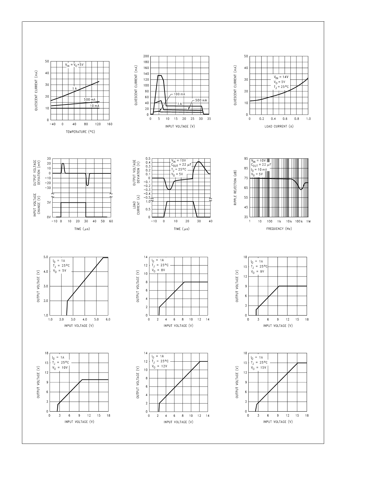
Typical Performance Characteristics
(Continued)
Quiescent Current
vs Temperature
DS008822-16
Quiescent Current
DS008822-17
Quiescent Current
DS008822-18
Line Transient Response
DS008822-19
Load Transient Response
DS008822-20
Ripple Rejection
DS008822-21
Low Voltage Behavior
DS008822-25
Low Voltage Behavior
DS008822-26
Low Voltage Behavior
DS008822-27
Low Voltage Behavior
DS008822-28
Low Voltage Behavior
DS008822-29
Low Voltage Behavior
DS008822-30
LM2940/LM2940C
www.national.com
7
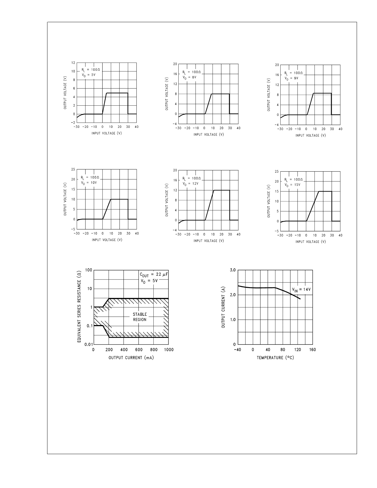
Typical Performance Characteristics
(Continued)
Output at
Voltage Extremes
DS008822-31
Output at
Voltage Extremes
DS008822-32
Output at
Voltage Extremes
DS008822-33
Output at
Voltage Extremes
DS008822-34
Output at
Voltage Extremes
DS008822-35
Output at
Voltage Extremes
DS008822-36
Output Capacitor ESR
DS008822-6
Peak Output Current
DS008822-8
LM2940/LM2940C
www.national.com
8
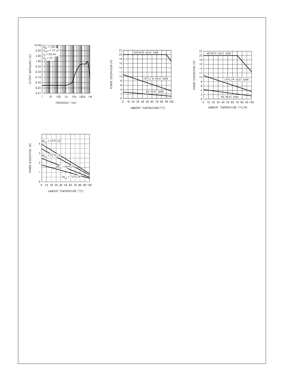
Typical Performance Characteristics
(Continued)
Output Impedance
DS008822-22
Maximum Power
Dissipation (TO-220)
DS008822-23
Maximum Power
Dissipation (TO-3)
DS008822-24
Maximum Power Dissipation
(TO-263) See (Note 2)
DS008822-10
LM2940/LM2940C
www.national.com
9
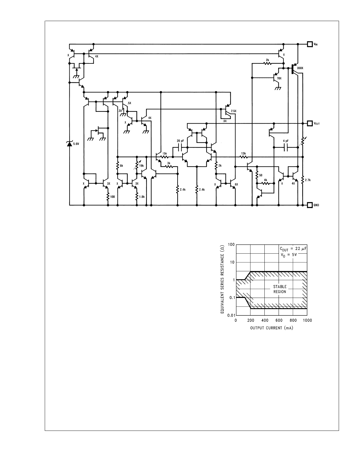
Equivalent Schematic Diagram
Application Hints
EXTERNAL CAPACITORS
The output capacitor is critical to maintaining regulator stabil-
ity, and must meet the required conditions for both ESR
(Equivalent Series Resistance) and minimum amount of ca-
pacitance.
MINIMUM CAPACITANCE:
The minimum output capacitance required to maintain stabil-
ity is 22 µF (this value may be increased without limit).
Larger values of output capacitance will give improved tran-
sient response.
ESR LIMITS:
The ESR of the output capacitor will cause loop instability if
it is too high or too low. The acceptable range of ESR plotted
versus load current is shown in the graph below.
It is essen-
tial that the output capacitor meet these requirements,
or oscillations can result.
It is important to note that for most capacitors, ESR is speci-
fied only at room temperature. However, the designer must
ensure that the ESR will stay inside the limits shown over the
entire operating temperature range for the design.
For aluminum electrolytic capacitors, ESR will increase by
about 30X as the temperature is reduced from 25˚C to
−40˚C. This type of capacitor is not well-suited for low tem-
perature operation.
Solid tantalum capacitors have a more stable ESR over tem-
perature, but are more expensive than aluminum electrolyt-
ics. A cost-effective approach sometimes used is to parallel
DS008822-1
Output Capacitor ESR
DS008822-6
FIGURE 1. ESR Limits
LM2940/LM2940C
www.national.com
10
Application Hints
(Continued)
an aluminum electrolytic with a solid Tantalum, with the total
capacitance split about 75/25% with the Aluminum being the
larger value.
If two capacitors are paralleled, the effective ESR is the par-
allel of the two individual values. The “flatter” ESR of the Tan-
talum will keep the effective ESR from rising as quickly at low
temperatures.
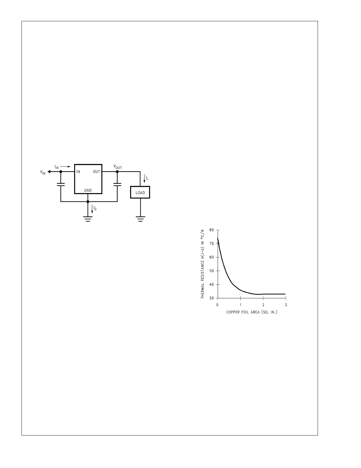
HEATSINKING
A heatsink may be required depending on the maximum
power dissipation and maximum ambient temperature of the
application. Under all possible operating conditions, the junc-
tion temperature must be within the range specified under
Absolute Maximum Ratings.
To determine if a heatsink is required, the power dissipated
by the regulator, P
D
, must be calculated.
The figure below shows the voltages and currents which are
present in the circuit, as well as the formula for calculating
the power dissipated in the regulator:
The next parameter which must be calculated is the maxi-
mum allowable temperature rise, T
R
(max). This is calcu-
lated by using the formula:
T
R
(max) = T
J
(max) − T
A
(max)
where: T
J
(max)
is the maximum allowable junction tem-
perature, which is 125˚C for commercial
grade parts.
T
A
(max)
is the maximum ambient temperature
which will be encountered in the applica-
tion.
Using the calculated values for T
R
(max) and P
D
, the maxi-
mum allowable value for the junction-to-ambient thermal re-
sistance,
θ
(J−A)
, can now be found:
θ
(J−A)
= T
R
(max)/P
D
IMPORTANT: If the maximum allowable value for
θ
(J−A)
is
found to be
≥
53˚C/W for the TO-220 package,
≥
80˚C/W for
the TO-263 package, or
≥
174˚C/W for the SOT-223 pack-
age, no heatsink is needed since the package alone will dis-
sipate enough heat to satisfy these requirements.
If the calculated value for
θ
(J−A)
falls below these limits, a
heatsink is required.
HEATSINKING TO-220 PACKAGE PARTS
The TO-220 can be attached to a typical heatsink, or se-
cured to a copper plane on a PC board. If a copper plane is
to be used, the values of
θ
(J−A)
will be the same as shown in
the next section for the TO-263.
If a manufactured heatsink is to be selected, the value of
heatsink-to-ambient thermal resistance,
θ
(H−A)
, must first be
calculated:
θ
(H−A)
=
θ
(J−A)
−
θ
(C−H)
−
θ
(J−C)
Where:
θ
(J−C)
is defined as the thermal resistance from
the junction to the surface of the case. A
value of 3˚C/W can be assumed for
θ
(J−C)
for this calculation.
θ
(C−H)
is defined as the thermal resistance be-
tween the case and the surface of the heat-
sink. The value of
θ
(C−H)
will vary from
about 1.5˚C/W to about 2.5˚C/W (depend-
ing on method of attachment, insulator,
etc.). If the exact value is unknown, 2˚C/W
should be assumed for
θ
(C−H)
.
When a value for
θ
(H−A)
is found using the equation shown,
a heatsink must be selected that has a value that is less than
or equal to this number.
θ
(H−A)
is specified numerically by the heatsink manufacturer
in the catalog, or shown in a curve that plots temperature rise
vs power dissipation for the heatsink.
HEATSINKING TO-263 AND SOT-223 PACKAGE PARTS
Both the TO-263 (“S”) and SOT-223 (“MP”) packages use a
copper plane on the PCB and the PCB itself as a heatsink.
To optimize the heat sinking ability of the plane and PCB,
solder the tab of the package to the plane.
Figure 3
shows for the TO-263 the measured values of
θ
(J−A)
for different copper area sizes using a typical PCB with 1
ounce copper
and no solder mask over the copper area used
for heatsinking.
As shown in the figure, increasing the copper area beyond 1
square inch produces very little improvement. It should also
be observed that the minimum value of
θ
(J−A)
for the TO-263
package mounted to a PCB is 32˚C/W.
As a design aid,
Figure 4
shows the maximum allowable
power dissipation compared to ambient temperature for the
TO-263 device (assuming
θ
(J−A)
is 35˚C/W and the maxi-
mum junction temperature is 125˚C).
DS008822-37
I
IN
= I
L
÷ I
G
P
D
= (V
IN
− V
OUT
) I
L
+ (V
IN
) I
G
FIGURE 2. Power Dissipation Diagram
DS008822-38
FIGURE 3.
θ
(J−A)
vs Copper (1 ounce) Area for the
TO-263 Package
LM2940/LM2940C
www.national.com
11
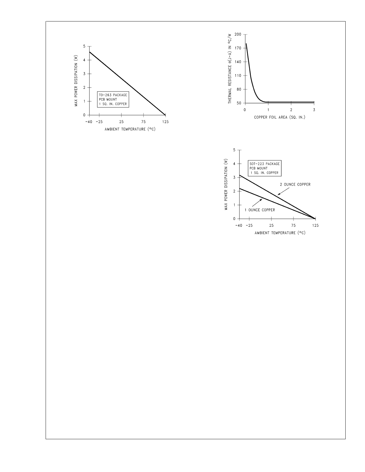
Application Hints
(Continued)
Figure 5
and
Figure 6
show the information for the SOT-223
package.
Figure 6
assumes a
θ
(J−A)
of 74˚C/W for 1 ounce
copper and 51˚C/W for 2 ounce copper and a maximum
junction temperature of 125˚C.
DS008822-39
FIGURE 4. Maximum Power Dissipation vs T
AMB
for
the TO-263 Package
DS008822-40
FIGURE 5.
θ
(J−A)
vs Copper (2 ounce) Area for the
SOT-223 Package
DS008822-41
FIGURE 6. Maximum Power Dissipation vs T
AMB
for
the SOT-223 Package
LM2940/LM2940C
www.national.com
12
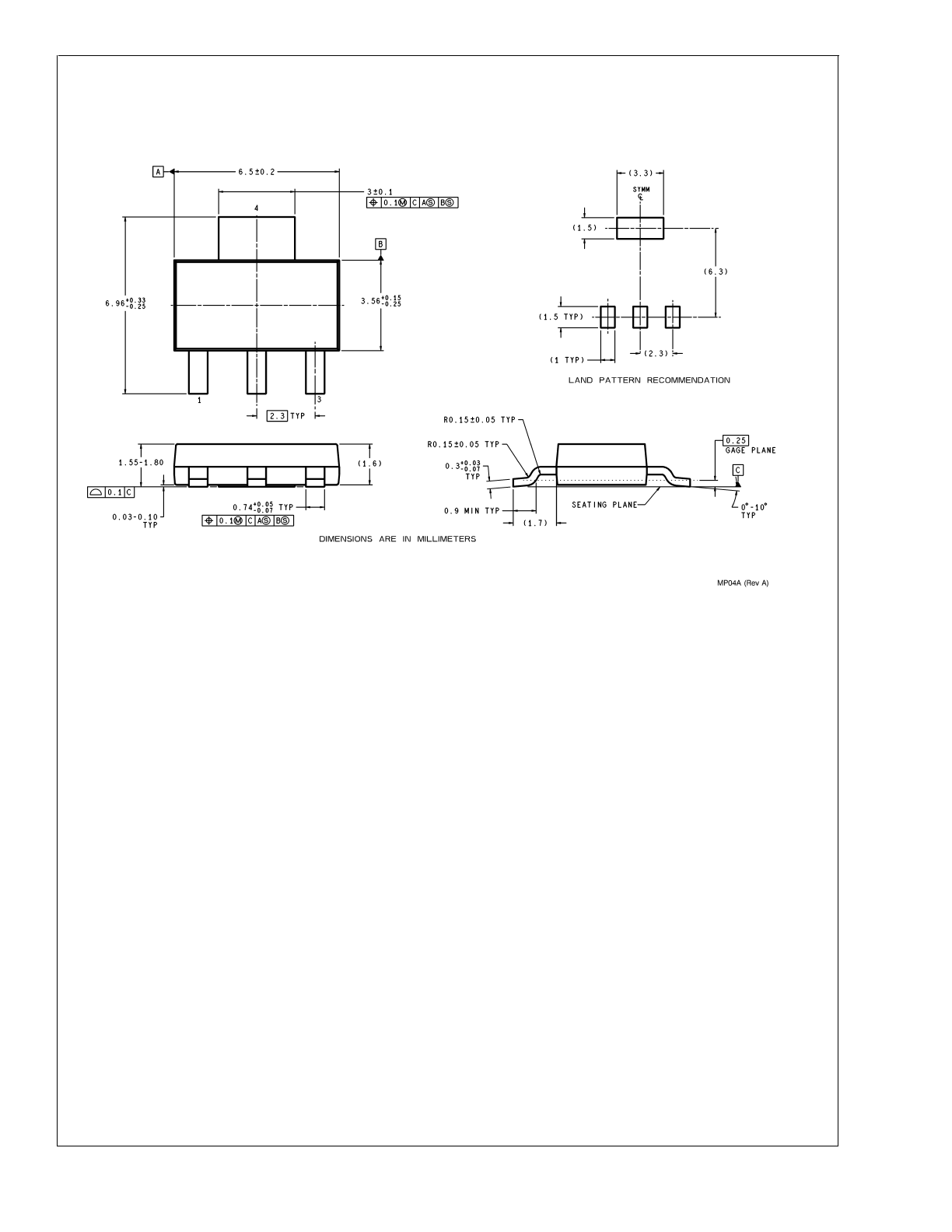
Physical Dimensions
inches (millimeters) unless otherwise noted
3-Lead SOT-223 Package
Order Part Number LM2940IMP-5.0
LM2940IMP-8.0 LM2940IMP-9.0
LM2940IMP-10 LM2940IMP-12 LM2940IMP-15
NS Package Number MP04A
LM2940/LM2940C
www.national.com
13
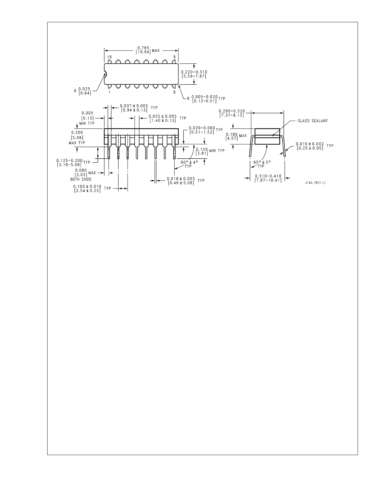
Physical Dimensions
inches (millimeters) unless otherwise noted (Continued)
16 Lead Dual-in-Line Package (J)
Order Number LM2940J-5.0/883 (5962-8958701EA),
LM2940J-8.0/883 (5962-9088301QEA),
LM2940J-12/883 (5962-9088401QEA),
LM2940J-15/883 (5962-9088501QEA)
See NS Package Number J16A
LM2940/LM2940C
www.national.com
14
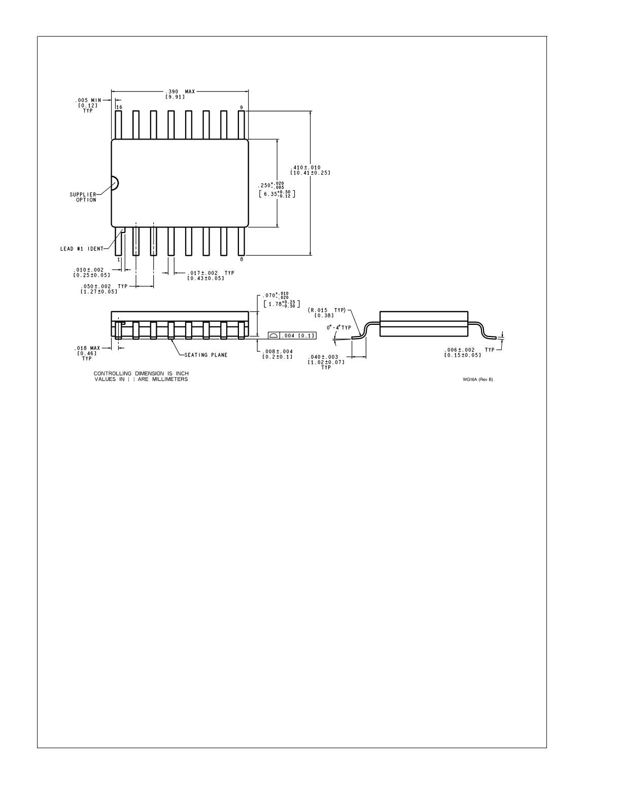
Physical Dimensions
inches (millimeters) unless otherwise noted (Continued)
16 Lead Surface Mount Package (WG)
Order Number LM2940WG5.0/883 (5962-8958701XA)
See NS Package Number WG16A
LM2940/LM2940C
www.national.com
15
Physical Dimensions
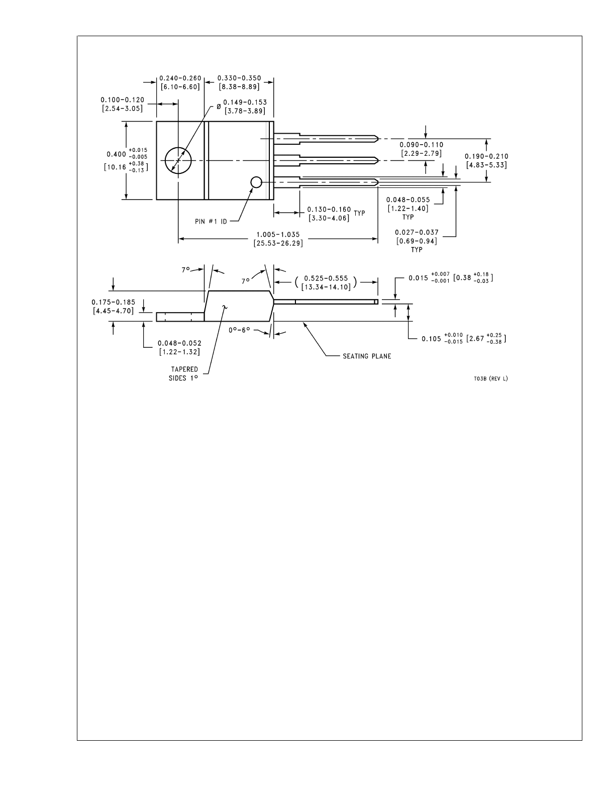
inches (millimeters) unless otherwise noted (Continued)
3-Lead TO-220 Plastic Package (T)
Order Number LM2940T-5.0, LM2940T-8.0,
LM2940T-9.0, LM2940T-10, LM2940T-12, LM2940CT-5.0,
LM2940CT-12 or LM2940CT-15
NS Package Number TO3B
LM2940/LM2940C
www.national.com
16
Physical Dimensions
inches (millimeters) unless otherwise noted (Continued)
LIFE SUPPORT POLICY
NATIONAL’S PRODUCTS ARE NOT AUTHORIZED FOR USE AS CRITICAL COMPONENTS IN LIFE SUPPORT
DEVICES OR SYSTEMS WITHOUT THE EXPRESS WRITTEN APPROVAL OF THE PRESIDENT AND GENERAL
COUNSEL OF NATIONAL SEMICONDUCTOR CORPORATION. As used herein:
1. Life support devices or systems are devices or
systems which, (a) are intended for surgical implant
into the body, or (b) support or sustain life, and
whose failure to perform when properly used in
accordance with instructions for use provided in the
labeling, can be reasonably expected to result in a
significant injury to the user.
2. A critical component is any component of a life
support device or system whose failure to perform
can be reasonably expected to cause the failure of
the life support device or system, or to affect its
safety or effectiveness.
National Semiconductor
Corporation
Americas
Tel: 1-800-272-9959
Fax: 1-800-737-7018
Email: support@nsc.com
National Semiconductor
Europe
Fax: +49 (0) 180-530 85 86
Email: europe.support@nsc.com
Deutsch Tel: +49 (0) 69 9508 6208
English
Tel: +44 (0) 870 24 0 2171
Français Tel: +33 (0) 1 41 91 8790
National Semiconductor
Asia Pacific Customer
Response Group
Tel: 65-2544466
Fax: 65-2504466
Email: ap.support@nsc.com
National Semiconductor
Japan Ltd.
Tel: 81-3-5639-7560
Fax: 81-3-5639-7507
www.national.com
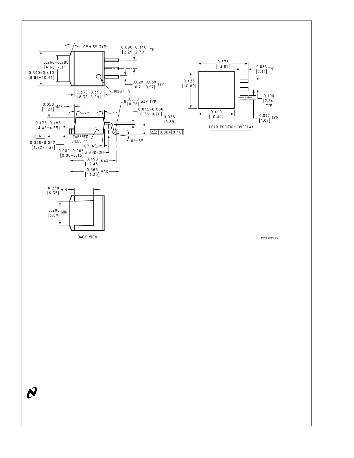
3-Lead TO-263 Surface Mount Package (MP)
Order Number LM2940S-5.0, LM2940S-8.0,
LM2940S-9.0, LM2940S-10, LM2940S-12,
LM2940CS-5.0, LM2940CS-12 or LM2940CS-15
NS Package Number TS3B
LM2940/LM2940C
1A
Low
Dropout
Regulator
National does not assume any responsibility for use of any circuitry described, no circuit patent licenses are implied and National reserves the right at any time without notice to change said circuitry and specifications.