
TL/F/11675
74VHC4046
CMOS
Phase
Lock
Loop
October 1995
74VHC4046
CMOS Phase Lock Loop
General Description
The 74VHC4046 is a low power phase lock loop utilizing
advanced silicon-gate CMOS technology to obtain high fre-
quency operation both in the phase comparator and VCO
sections. This device contains a low power linear voltage
controlled oscillator (VCO), a source follower, and three
phase comparators. The three phase comparators have a
common signal input and a common comparator input. The
signal input has a self biasing amplifier allowing signals to
be either capacitively coupled to the phase comparators
with a small signal or directly coupled with standard input
logic levels. This device is similar to the CD4046 except that
the Zener diode of the metal gate CMOS device has been
replaced with a third phase comparator.
Phase Comparator I is an exclusive OR (XOR) gate. It pro-
vides a digital error signal that maintains a 90 phase shift
between the VCO’s center frequency and the input signal
(50% duty cycle input waveforms). This phase detector is
more susceptible to locking onto harmonics of the input fre-
quency than phase comparator I, but provides better noise
rejection.
Phase comparator III is an SR flip-flop gate. It can be used
to provide the phase comparator functions and is similar to
the first comparator in performance.
Phase comparator II is an edge sensitive digital sequential
network. Two signal outputs are provided, a comparator out-
put and a phase pulse output. The comparator output is a
TRI-STATE
É
output that provides a signal that locks the
VCO output signal to the input signal with 0 phase shift be-
tween them. This comparator is more susceptible to noise
throwing the loop out of lock, but is less likely to lock onto
harmonics than the other two comparators.
In a typical application any one of the three comparators
feed an external filter network which in turn feeds the VCO
input. This input is a very high impedance CMOS input
which also drives the source follower. The VCO’s operating
frequency is set by three external components connected to
the C1A, C1B, R1 and R2 pins. An inhibit pin is provided to
disable the VCO and the source follower, providing a meth-
od of putting the IC in a low power state.
The source follower is a MOS transistor whose gate is con-
nected to the VCO input and whose drain connects the De-
modulator output. This output normally is used by tying a
resistor from pin 10 to ground, and provides a means of
looking at the VCO input without loading down modifying the
characteristics of the PLL filter.
Features
Y
Low dynamic power consumption
(V
CC
e
4.5V)
Y
Maximum VCO operating frequency:
12 MHz
(V
CC
e
4.5V)
Y
Fast comparator response time (V
CC
e
4.5V)
Comparator I:
25 ns
Comparator II:
30 ns
Comparator III:
25 ns
Y
VCO has high linearity and high temperature stability
Y
Pin and function compatible with the 74HC4046
Commercial
Package
Package Description
Number
74VHC4046M
M16A
16-Lead Molded JEDEC SOIC
74VHC4046N
N16E
16-Lead Molded DIP
Note:
Surface mount packages are also available on Tape and Reel. Specify by appending the suffix letter ‘‘X’’ to the ordering code.
TRI-STATE
É
is a registered trademark of National Semiconductor Corporation.
C1995 National Semiconductor Corporation
RRD-B30M125/Printed in U. S. A.
Block and Connection Diagrams
TL/F/11675 – 1
Pin Assignment for
SOIC and PDIP
TL/F/11675 – 2
2
Absolute Maximum Ratings
(Notes 1 & 2)
Supply Voltage (V
CC
)
b
0.5 to
a
7.0V
DC Input Voltage (V
IN
)
b
1.5 to V
CC
a
1.5V
DC Output Voltage (V
OUT
)
b
0.5 to V
CC
a
0.5V
Clamp Diode Current (I
IK
, I
OK
)
g
20 mA
DC Output Current per pin (I
OUT
)
g
25 mA
DC V
CC
or GND Current, per pin (I
CC
)
g
50 mA
Storage Temperature Range (T
STG
)
b
65
§
C
a
150
§
C
Power Dissipation (P
D
)
(Note 3)
600 mW
S.O. Package only
500 mW
Lead Temperature (T
L
)
(Soldering 10 seconds)
260
§
C
Operating Conditions
Min
Max
Units
Supply Voltage (V
CC
)
2
6
V
DC Input or Output Voltage
0
V
CC
V
(V
IN
, V
OUT
)
Operating Temp. Range (T
A
)
74VHC
b
40
a
85
§
C
Input Rise or Fall Times
(t
r
, t
f
)
V
CC
e
2.0V
1000
ns
V
CC
e
4.5V
500
ns
V
CC
e
6.0V
400
ns
DC Electrical Characteristics
(Note 4)
T
A
e
25
§
C
74VHC
Symbol
Parameter
Conditions
V
CC
T
A
e b
40 to 85
§
C
Units
Typ
Guaranteed Limits
V
IH
Minimum High Level Input
2.0V
1.5
1.5
V
Voltage
4.5V
3.15
3.15
V
6.0V
4.2
4.2
V
V
IL
Maximum Low Level Input
2.0V
0.5
0.5
V
Voltage
4.5V
1.35
1.35
V
6.0V
1.8
1.8
V
V
OH
Minimum High Level Output
V
IN
e
V
IH
or V
IL
Voltage
l
I
OUT
l
s
20 mA
2.0V
2.0
1.9
1.9
V
4.5V
4.5
4.4
4.4
V
6.0V
6.0
5.9
5.9
V
V
IN
e
V
IH
or V
IL
l
I
OUT
l
s
4.0 mA
4.5V
4.2
3.98
3.84
V
l
I
OUT
l
s
5.2 mA
6.0V
5.7
5.48
5.34
V
V
OL
Maximum Low Level Output
V
IN
e
V
IH
or V
IL
Voltage
l
I
OUT
l
s
20 mA
2.0V
0
0.1
0.1
V
4.5V
0
0.1
0.1
V
6.0V
0
0.1
0.1
V
V
IN
e
V
IH
or V
IL
l
I
OUT
l
s
4.0 mA
4.5V
0.2
0.26
0.33
V
l
I
OUT
l
s
5.2 mA
6.0V
0.2
0.26
0.33
V
I
IN
Maximum Input Current (Pins 3,5,9)
V
IN
e
V
CC
or GND
6.0V
g
0.1
g
1.0
m
A
I
IN
Maximum Input Current (Pin 14)
V
IN
e
V
CC
or GND
6.0V
20
50
80
m
A
I
OZ
Maximum TRI-STATE Output
V
OUT
e
V
CC
or GND
6.0V
g
0.25
g
2.5
m
A
Leakage Current (Pin 13)
I
CC
Maximum Quiescent Supply
V
IN
e
V
CC
or GND
6.0V
30
40
65
m
A
Current
I
OUT
e
0 mA
V
IN
e
V
CC
or GND
6.0V
600
750
1200
m
A
Pin 14 Open
Note 1:
Maximum Ratings are those values beyond which damage to the device may occur.
Note 2:
Unless otherwise specified all voltages are referenced to ground.
Note 3:
Power Dissipation temperature derating Ð plastic ‘‘N’’ package: b12 mW/
§
C from 65
§
C to 85
§
C.
Note 4:
For a power supply of 5V
g
10% the worst case output voltages (V
OH
, and V
OL
) occur for VHC at 4.5V. Thus the 4.5V values should be used when
designing with this supply. Worst case V
IH
and V
IL
occur at V
CC
e
5.5V and 4.5V respectively. (The V
IH
value at 5.5V is 3.85V.) The worst case leakage current (I
IN
,
I
CC
, and I
OZ
) occur for CMOS at the higher voltage and so the 6.0V values should be used.
3
AC Electrical Characteristics
V
CC
e
2.0 to 6.0V, CL
e
50 pF, t
r
e
t
f
e
6 ns (unless otherwise specified.)
Symbol
Parameters
Conditions
V
CC
T
e
25C
74VHC
Units
Typ
Guaranteed Limits
AC Coupled
C (series)
e
100 pF
2.0V
25
100
150
mV
Input Sensitiv-
f
IN
e
500 kHz
4.5V
50
150
200
mV
ity, Signal In
6.0V
135
250
300
mV
t
r
, t
f
Maximum Output
2.0V
30
75
95
ns
Rise and Fall
4.5V
9
15
19
ns
Time
6.0V
8
12
15
ns
C
IN
Maximum Input
7
pF
Capacitance
Phase Comparator I
t
PHL
, t
PLH
Maximum Prop-
3.3V
65
117
146
ns
agation Delay
4.5V
25
40
50
ns
6.0V
20
34
43
ns
Phase Comparator II
t
PZL
Maximum TRI-
3.3V
75
130
160
ns
STATE Enable
4.5V
25
45
56
ns
Time
6.0V
22
38
48
ns
t
PZH
, t
PHZ
Maximum TRI-
3.3V
88
140
175
ns
STATE Enable
4.5V
30
48
60
ns
Time
6.0V
25
41
51
ns
t
PLZ
Maximum TRI-
3.3V
90
140
175
ns
STATE Disable
4.5V
32
48
60
ns
Time
6.0V
28
41
51
ns
t
PHL
, t
PLH
Maximum Prop-
3.3V
100
146
180
ns
agation Delay
4.5V
34
50
63
ns
High to Low
6.0V
27
43
53
ns
to Phase Pulses
Phase Comparator III
t
PHL
, t
PLH
Maximum Prop-
3.3V
75
117
146
ns
agation Delay
4.5V
25
40
50
ns
6.0V
22
34
43
ns
C
PD
Maximum Power
All Comparators
130
pF
Dissipation
V
IN
e
V
CC
and GND
Capacitance
Voltage Controlled Oscillator (Specified to operate from V
CC
e
3.0V to 6.0V)
f
MAX
Maximum
C1
e
50 pF
Operating
R1
e
100X
4.5V
7
4.5
MHz
Frequency
R2
e
%
6.0V
11
7
MHz
VCO
in
e
V
CC
C1
e
0 pF
4.5V
12
MHz
R1
e
100X
6.0
14
MHz
VCO
in
e
V
CC
Duty Cycle
50
%
Demodulator Output
Offset Voltage
R
s
e
20 kX
4.5V
0.75
1.3
1.5
V
VCO
in
– V
dem
Offset
R
s
e
20 kX
4.5V
Variation
VCO
in
e
1.75V
0.65
V
2.25V
0.1
2.75V
0.75
4
Typical Performance Characteristics
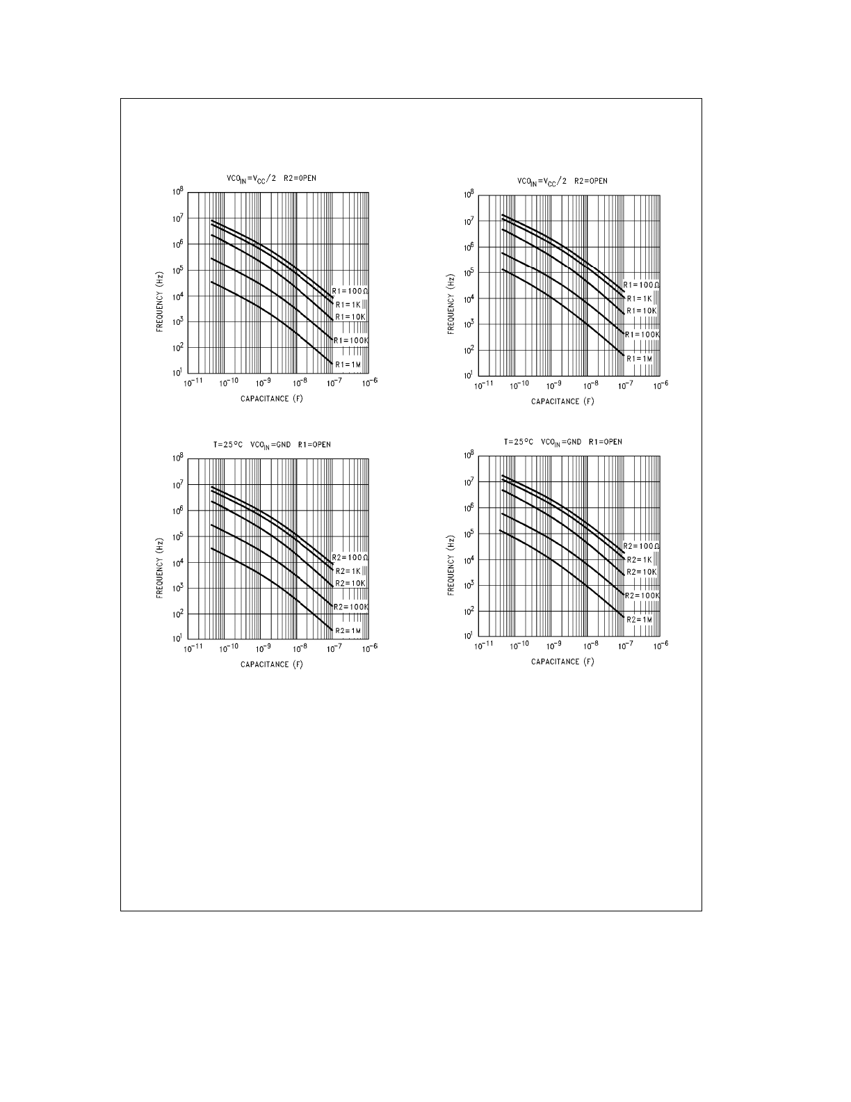
Typical Center Frequency
vs R1, C1
V
CC
e
4.5V
TL/F/11675 – 3
Typical Center Frequency
vs R1, C1
V
CC
e
6V
TL/F/11675 – 4
Typical Offset Frequency
vs R2, C1
V
CC
e
4.5V
TL/F/11675 – 5
Typical Offset Frequency
vs R2, C1
V
CC
e
6V
TL/F/11675 – 6
5
Typical Performance Characteristics
(Continued)
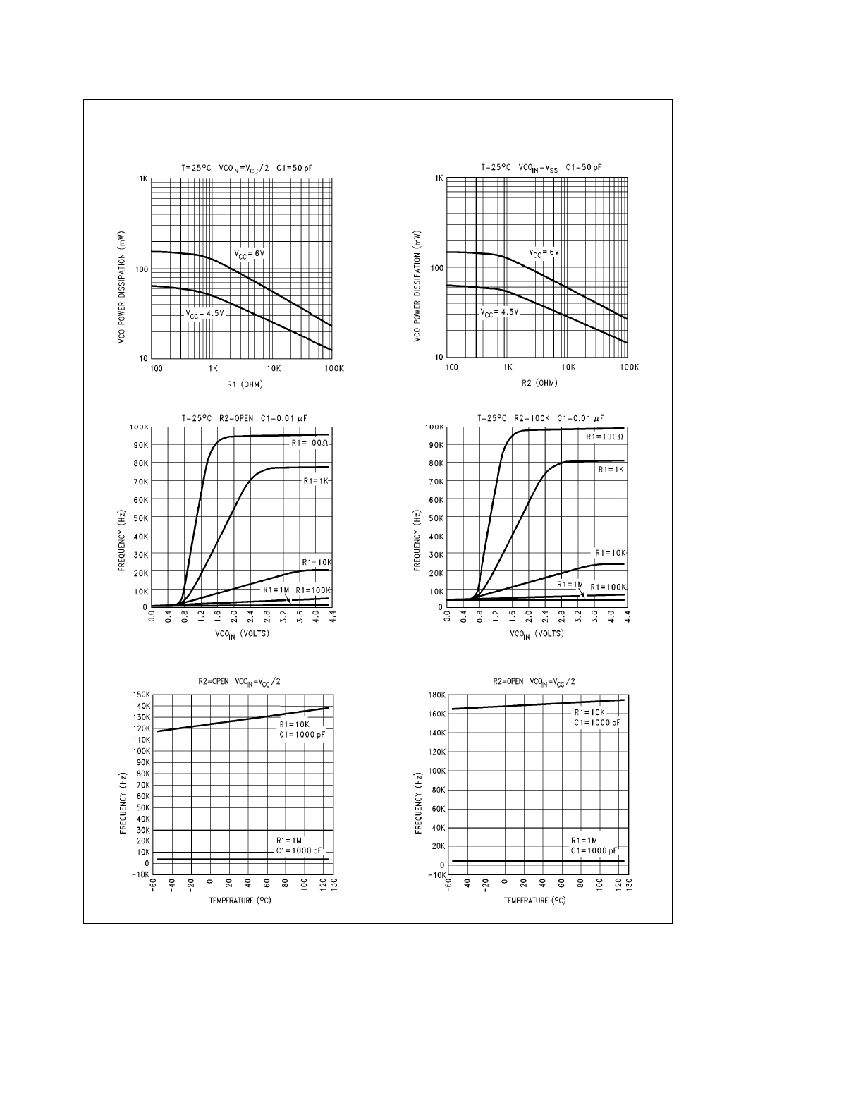
VHC4046 Typical VCO Power Dissipation
@
Center Frequency vs R1
TL/F/11675 – 7
VHC4046 Typical VCO Power
Dissipation
@
f
min
vs R2
TL/F/11675 – 8
VHC4046 VCO
in
vs f
out
V
CC
e
4.5V
TL/F/11675 – 9
VHC4046 VCO
in
vs f
out
V
CC
e
4.5V
TL/F/11675 – 10
VHC4046 VCO
out
vs
Temperature
V
CC
e
4.5V
TL/F/11675 – 11
VHC4046 VCO
out
vs
Temperature
V
CC
e
6V
TL/F/11675 – 12
6
Typical Performance Characteristics
(Continued)
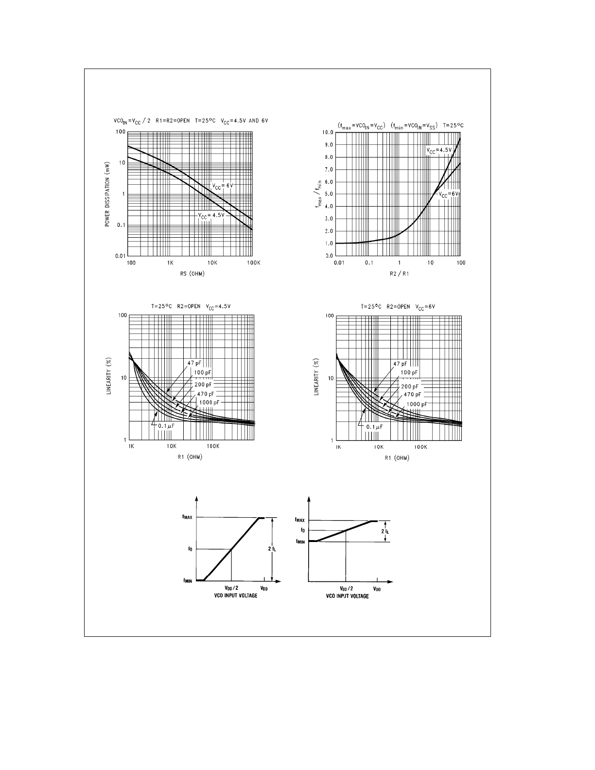
VHC4046 Typical Source Follower
Power Dissipation vs RS
TL/F/11675 – 13
Typical f
max
/f
min
vs R2/R1
V
CC
e
4.5V & 6V f
max
/f
min
TL/F/11675 – 14
VHC4046 Typical VCO Linearity vs R1 & C1
TL/F/11675 – 15
VHC4046 Typical VCO Linearity vs R1 & C1
TL/F/11675 – 16
VCO WITHOUT OFFSET
R2
e
%
VCO WITH OFFSET
(a)
TL/F/11675 – 17
FIGURE 1
7
Comparator I
Comparator II & III
R
2
e
%
R
2
i
%
R
2
e
%
R
2
i
%
– Given: f
0
– Given: f
0
and f
L
– Given: f
max
– Given: f
min
and f
max
– Use f
0
with curve titled
– Calculate f
min
from the
– Calculate f
0
from the
– Use f
min
with curve titled
center frequency vs R1, C
equation f
min
e
f
o
b
f
L
equation f
o
e
f
max
/2
offset frequency vs R2,
to determine R1 and C1
– Use f
min
with curve titled
– Use f
0
with curve titled
C to determine R2 and C1
offset frequency vs R2, C
center frequency vs R1, C
– Calculate f
max
/f
min
to determine R2 and C1
to determine R1 and C1
– Use f
max
/f
min
with curve
– Calculate f
max
/f
min
from
titled f
max
/f
min
vs R2/R1
the equation f
max
/f
min
e
to determine ratio R2/R1
f
o
a
f
L
/f
o
b
f
L
to obtain R1
– Use f
max
/f
min
with curve
titled f
max
/f
min
vs R2/R1
to determine ratio R2/R1
to obtain R1
(b)
FIGURE 1
(Continued)
Detailed Circuit Description
VOLTAGE CONTROLLED OSCILLATOR/SOURCE
FOLLOWER
The VCO requires two or three external components to op-
erate. These are R1, R2, C1. Resistor R1 and capacitor C1
are selected to determine the center frequency of the VCO.
R1 controls the lock range. As R1’s resistance decreases
the range of f
min
to f
max
increases. Thus the VCO’s gain
decreases. As C1 is changed the offset (if used) of R2, and
the center frequency is changed. (See typical performance
curves) R2 can be used to set the offset frequency with 0V
at VCO input. If R2 is omitted the VCO range is from 0Hz. As
R2 is decreased the offset frequency is increased. The ef-
fect of R2 is shown in the design information table and typi-
cal performance curves. By increasing the value of R2 the
lock range of the PLL is offset above 0Hz and the gain
(Volts/rad.) does not change. In general, when offset is de-
sired, R2 and C1 should be chosen first, and then R1 should
be chosen to obtain the proper center frequency.
Internally the resistors set a current in a current mirror as
shown in
Figure 1
. The mirrored current drives one side of
TL/F/11675 – 18
FIGURE 2. Logic Diagram for VCO
8
Detailed Circuit Description
(Continued)
the capacitor once the capacitor charges up to the thresh-
old of the schmitt trigger the oscillator logic flips the capaci-
tor over and causes the mirror to charge the opposite side
of the capacitor. The output from the internal logic is then
taken to pin 4.
The input to the VCO is a very high impedance CMOS input
and so it will not load down the loop filter, easing the filters
design. In order to make signals at the VCO input accessible
without degrading the loop performance a source follower
transistor is provided. This transistor can be used by con-
necting a resistor to ground and its drain output will follow
the VCO input signal.
An inhibit signal is provided to allow disabling of the VCO
and the source follower. This is useful if the internal VCO is
not being used. A logic high on inhibit disables the VCO and
source follower.
The output of the VCO is a standard high speed CMOS
output with an equivalent LSTTL fanout of 10. The VCO
output is approximately a square wave. This output can ei-
ther directly feed the comparator input of the phase compar-
ators or feed external prescalers (counters) to enable fre-
quency synthesis.
PHASE COMPARATORS
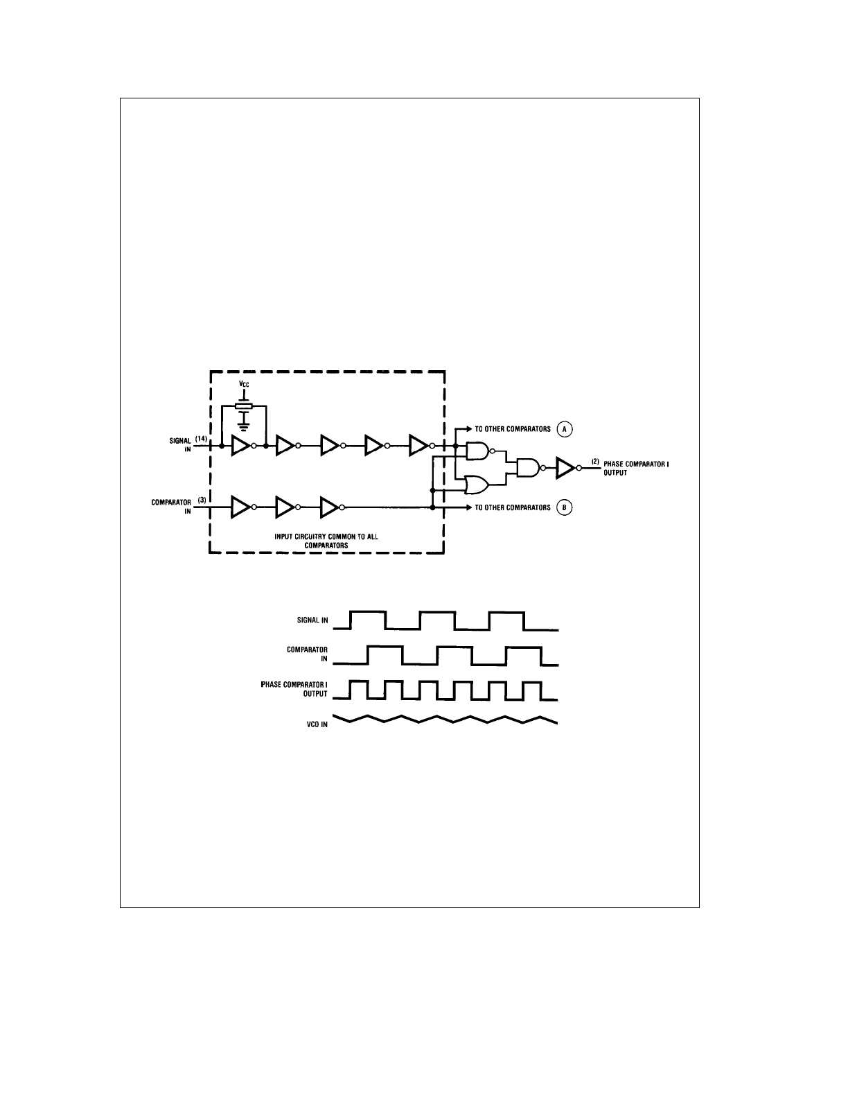
All three phase comparators share two inputs, Signal In and
Comparator In. The Signal In has a special DC bias network
that enables AC coupling of input signals. If the signals are
not AC coupled then this input requires logic levels the
same as standard 74VHC. The Comparator input is a stan-
dard digital input. Both input structures are shown in
Figure
3
.
The outputs of these comparators are essentially standard
74VHC voltage outputs. (Comparator II is TRI-STATE.)
TL/F/11675-19
FIGURE 3. Logic Diagram for Phase Comparator I and the Common Input Circuit for All Three Comparators
TL/F/11675 – 20
FIGURE 4. Typical Phase Comparator I. Waveforms
9
Detailed Circuit Description
(Continued)
Thus in normal operation V
CC
and ground voltage levels are
fed to the loop filter. This differs from some phase detectors
which supply a current output to the loop filter and this
should be considered in the design. (The CD4046 also pro-
vides a voltage.)
Figure 5
shows the state tables for all three comparators.
PHASE COMPARATOR I
This comparator is a simple XOR gate similar to the
54/74HC86, and its operation is similar to an overdriven
balanced modulator. To maximize lock range the input fre-
quencies must have a 50% duty cycle. Typical input and
output waveforms are shown in
Figure 4
. The output of the
phase detector feeds the loop filter which averages the out-
put voltage. The frequency range upon which the PLL will
lock onto if initially out of lock is defined as the capture
range. The capture range for phase detector I is dependent
on the loop filter employed. The capture range can be as
large as the lock range which is equal to the VCO frequency
range.
To see how the detector operates refer to
Figure 4
. When
two square wave inputs are applied to this comparator, an
output waveform whose duty cycle is dependent on the
phase difference between the two signals results. As the
phase difference increases the output duty cycle increases
and the voltage after the loop filter increases. Thus in order
to achieve lock, when the PLL input frequency increases the
VCO input voltage must increase and the phase difference
between comparator in and signal in will increase. At an
input frequency equal f
min
, the VCO input is at 0V and this
requires the phase detector output to be ground hence the
two input signals must be in phase. When the input frequen-
cy is f
max
then the VCO input must be V
CC
and the phase
detector inputs must be 180
§
out of phase.
The XOR is more susceptible to locking onto harmonics of
the signal input than the digital phase detector II. This can
be seen by noticing that a signal 2 times the VCO frequency
results in the same output duty cycle as a signal equal the
VCO frequency. The difference is that the output frequency
of the 2f example is twice that of the other example. The
loop filter and the VCO range should be designed to prevent
locking on to harmonics.
PHASE COMPARATOR II
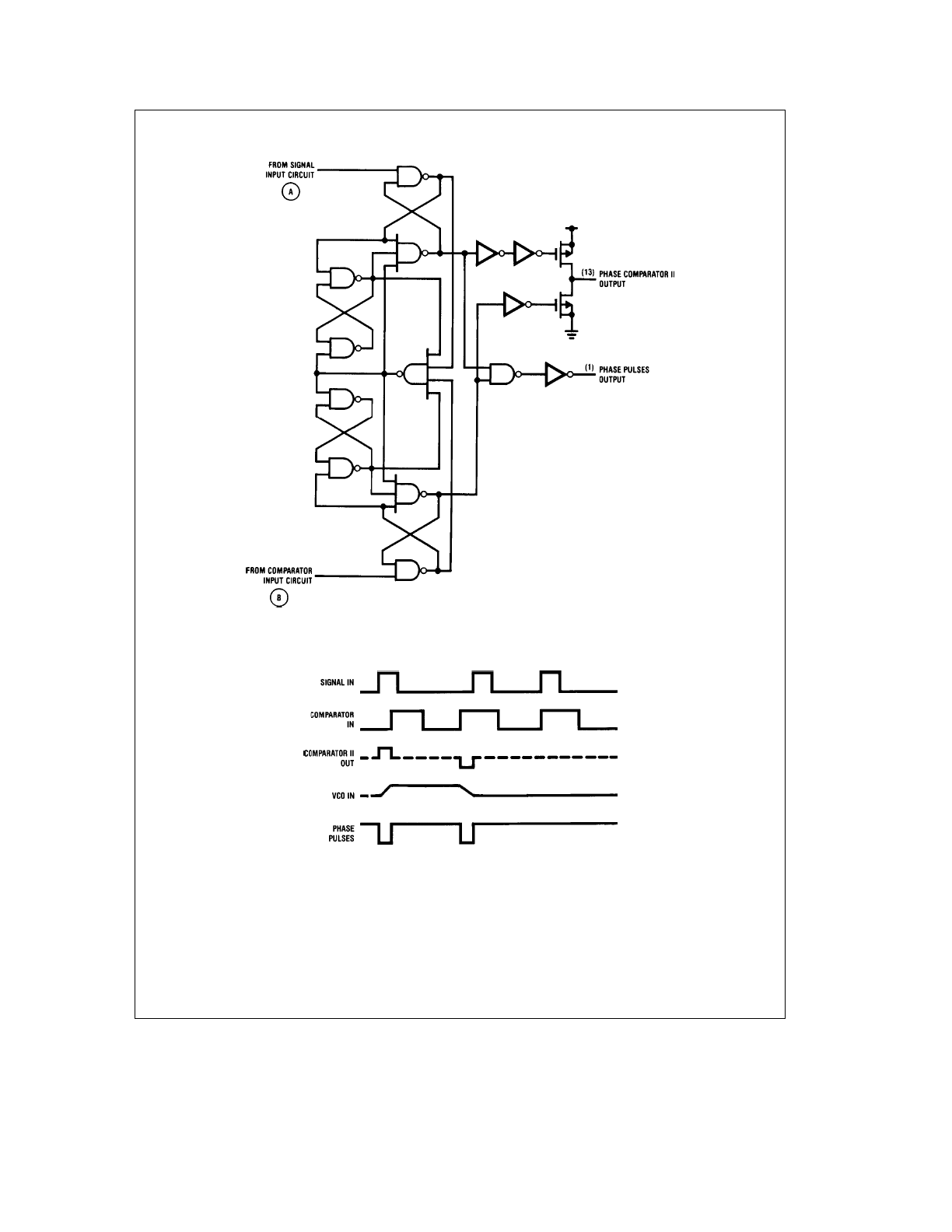
This detector is a digital memory network. It consists of four
flip-flops and some gating logic, a three state output and a
phase pulse output as shown in
Figure 6
. This comparator
acts only on the positive edges of the input signals and is
thus independent of signal duty cycle.
Phase comparator II operates in such a way as to force the
PLL into lock with 0 phase difference between the VCO
output and the signal input positive waveform edges.
Figure
7
shows some typical loop waveforms. First assume that
the signal input phase is leading the comparator input. This
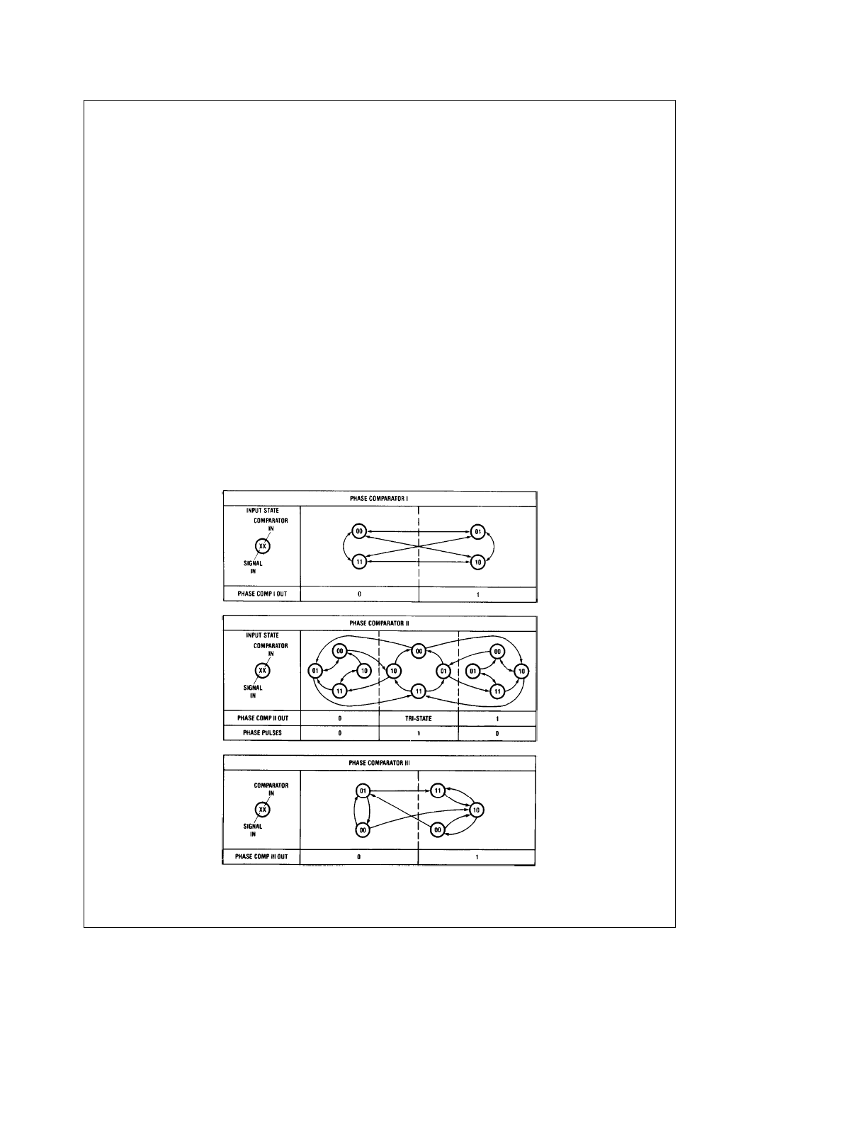
Phase Comparator State Diagrams
TL/F/11675 – 21
FIGURE 5. PLL State Tables
10
Detailed Circuit Description
(Continued)
TL/F/11675 – 22
FIGURE 6. Logic Diagram for Phase Comparator II
TL/F/11675 – 23
FIGURE 7. Typical Phase Comparator II Output Waveforms
11
Detailed Circuit Description
(Continued)
means that the VCO’s frequency must be increased to bring
its leading edge into proper phase alignment. Thus the
phase detector II output is set high. This will cause the loop
filter to charge up the VCO input increasing the VCO fre-
quency. Once the leading edge of the comparator input is
detected the output goes TRI-STATE holding the VCO input
at the loop filter voltage. If the VCO still lags the signal then
the phase detector will again charge up to VCO input for the
time between the leading edges of both waveforms.
If the VCO leads the signal then when the leading edge of
the VCO is seen the output of the phase comparator goes
low. This discharges the loop filter until the leading edge of
the signal is detected at which time the output TRI-STATE
itself again. This has the effect of slowing down the VCO to
again make the rising edges of both waveform coincident.
When the PLL is out of lock the VCO will be running either
slower or faster than the signal input. If it is running slower
the phase detector will see more signal rising edges and so
the output of the phase comparator will be high a majority of
the time, raising the VCO’s frequency. Conversely, if the
VCO is running faster than the signal the output of the de-
tector will be low most of the time and the VCO’s output
frequency will be decreased.
As one can see when the PLL is locked the output of phase
comparator II will be almost always TRI-STATE except for
minor corrections at the leading edge of the waveforms.
When the detector is TRI-STATE the phase pulse output is
high. This output can be used to determine when the PLL is
in the locked condition.
This detector has several interesting characteristics. Over
the entire VCO frequency range there is no phase differ-
ence between the comparator input and the signal input.
The lock range of the PLL is the same as the capture range.
Minimal power is consumed in the loop filter since in lock
the detector output is a high impedance. Also when no sig-
nal is present the detector will see only VCO leading edges,
and so the comparator output will stay low forcing the VCO
to f
min
operating frequency.
Phase comparator II is more susceptible to noise causing
the phase lock loop to unlock. If a noise pulse is seen on the
signal input, the comparator treats it as another positive
edge of the signal and will cause the output to go high until
the VCO leading edge is seen, potentially for a whole signal
input period. This would cause the VCO to speed up during
that time. When using the phase comparator I the output of
that phase detector would be disturbed for only the short
duration of the noise spike and would cause less upset.
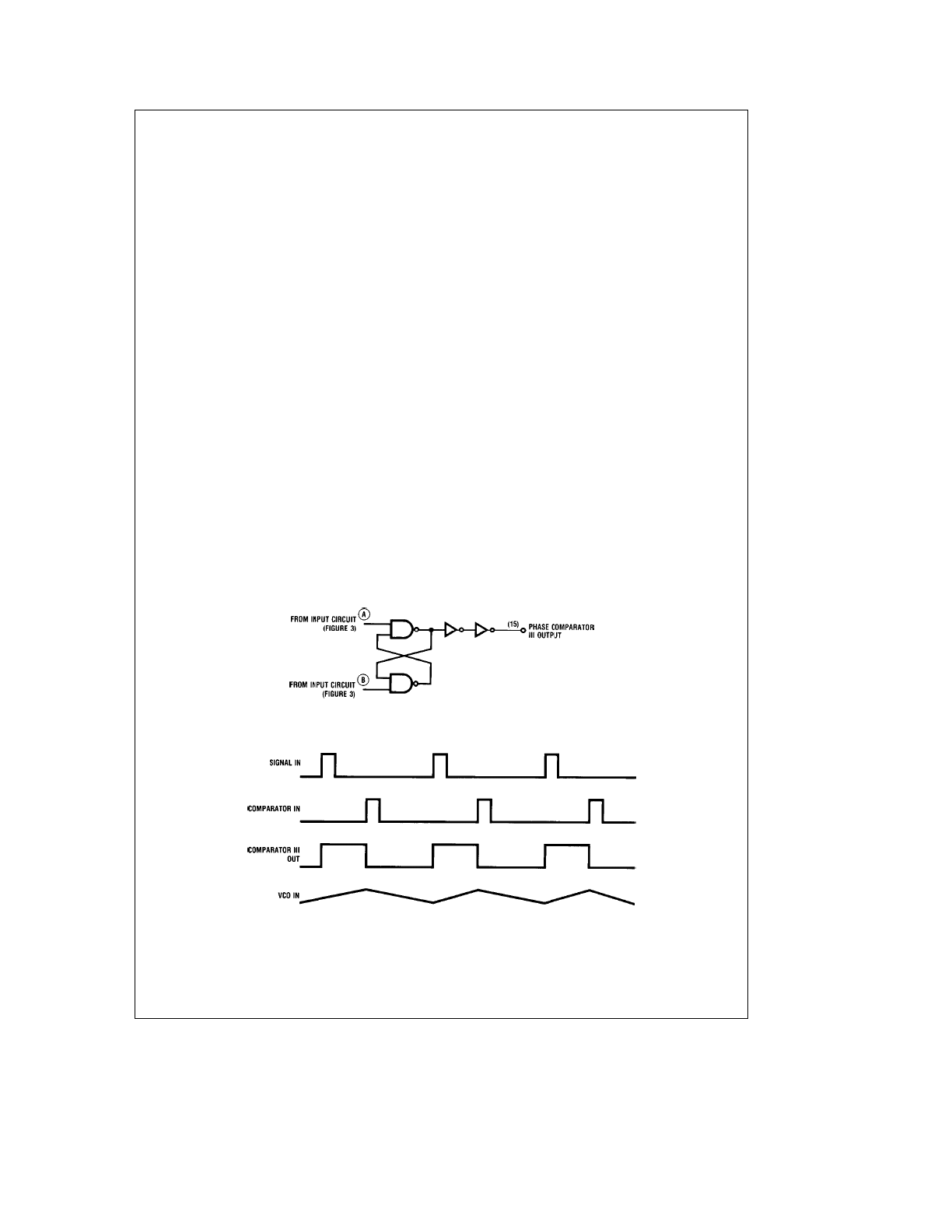
PHASE COMPARATOR III
This comparator is a simple S-R Flip-Flop which can func-
tion as a phase comparator
Figure 8
. It has some similar
characteristics to the edge sensitive comparator. To see
how this detector works assume input pulses are applied to
the signal and comparator inputs as shown in
Figure 9
.
When the signal input leads the comparator input the flop is
set. This will charge up the loop filter and cause the VCO to
speed up, bringing the comparator into phase with the sig-
nal input. When using short pulses as input this comparator
behaves very similar to the second comparator. But one can
see that if the signal input is a long pulse, the output of the
comparator will be forced to a one no matter how many
comparator input pulses are received. Also if the VCO input
is a square wave (as it is) and the signal input is pulse then
the VCO will force the comparator output low much of the
time. Therefore it is ideal to condition the signal and com-
parator input to short pulses. This is most easily done by
using a series capacitor.
TL/F/11675 – 24
FIGURE 8. Phase Comparator III Logic Diagram
TL/F/11675 – 25
FIGURE 9. Typical Waveforms for Phase Comparator III
12
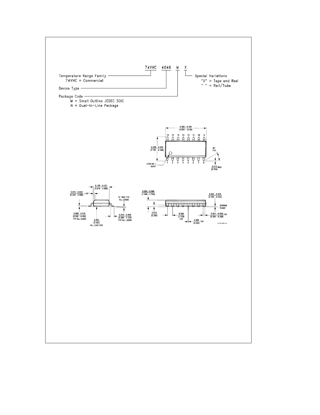
Ordering Information
The device number is used to form part of a simplified purchasing code where the package type and temperature range are
defined as follows:
TL/F/11675 – 26
Physical Dimensions
inches (millimeters)
16-Lead (0.150
×
Wide) Molded Small Outline Package, JEDEC
Order Number 74VHC4046M
NS Package Number M16A
13
74VHC4046
CMOS
Phase
Lock
Loop
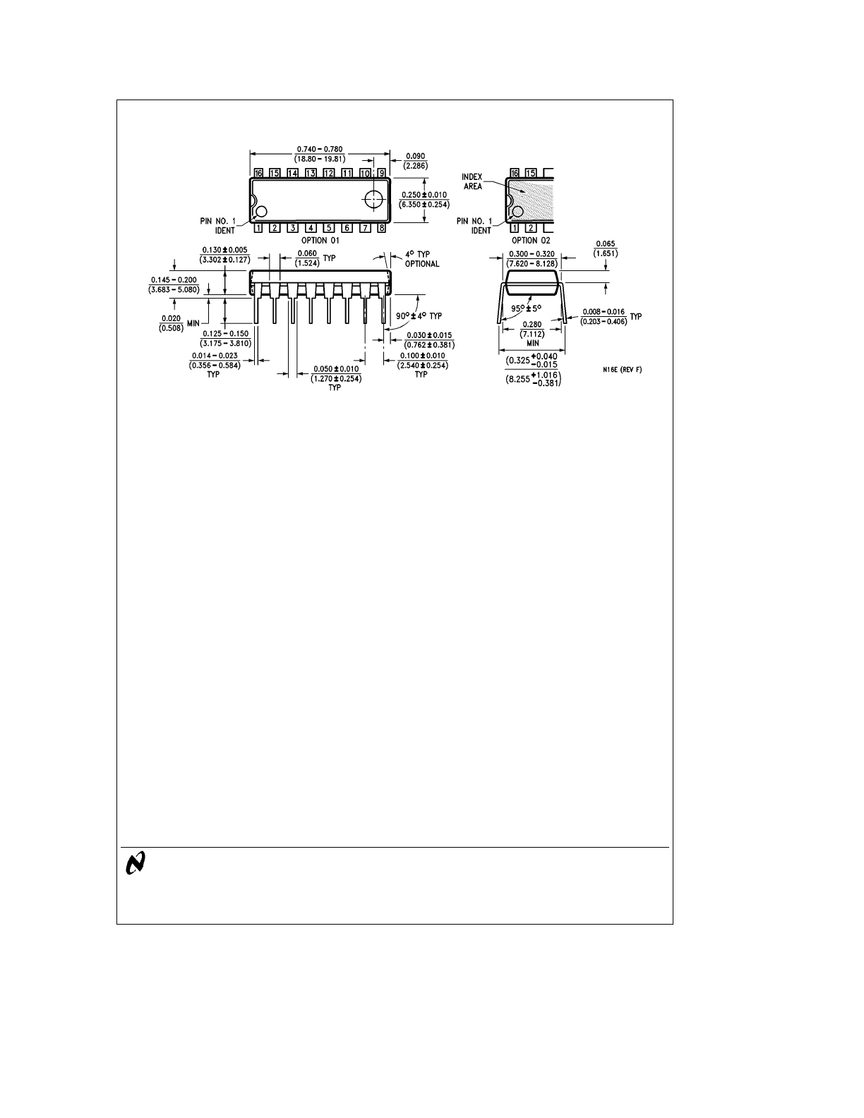
Physical Dimensions
inches (millimeters) (Continued)
Molded Dual-In-Line Package (N)
Order Number 74VHC4046N
NS Package Number N16E
LIFE SUPPORT POLICY
NATIONAL’S PRODUCTS ARE NOT AUTHORIZED FOR USE AS CRITICAL COMPONENTS IN LIFE SUPPORT
DEVICES OR SYSTEMS WITHOUT THE EXPRESS WRITTEN APPROVAL OF THE PRESIDENT OF NATIONAL
SEMICONDUCTOR CORPORATION. As used herein:
1. Life support devices or systems are devices or
2. A critical component is any component of a life
systems which, (a) are intended for surgical implant
support device or system whose failure to perform can
into the body, or (b) support or sustain life, and whose
be reasonably expected to cause the failure of the life
failure to perform, when properly used in accordance
support device or system, or to affect its safety or
with instructions for use provided in the labeling, can
effectiveness.
be reasonably expected to result in a significant injury
to the user.
National Semiconductor
National Semiconductor
National Semiconductor
National Semiconductor
Corporation
Europe
Hong Kong Ltd.
Japan Ltd.
1111 West Bardin Road
Fax: (
a
49) 0-180-530 85 86
13th Floor, Straight Block,
Tel: 81-043-299-2309
Arlington, TX 76017
Email: cnjwge
@
tevm2.nsc.com
Ocean Centre, 5 Canton Rd.
Fax: 81-043-299-2408
Tel: 1(800) 272-9959
Deutsch Tel: (
a
49) 0-180-530 85 85
Tsimshatsui, Kowloon
Fax: 1(800) 737-7018
English
Tel: (
a
49) 0-180-532 78 32
Hong Kong
Fran
3ais Tel: (
a
49) 0-180-532 93 58
Tel: (852) 2737-1600
Italiano
Tel: (
a
49) 0-180-534 16 80
Fax: (852) 2736-9960
National does not assume any responsibility for use of any circuitry described, no circuit patent licenses are implied and National reserves the right at any time without notice to change said circuitry and specifications.