
TL/F/11520
74VHC245
#
74VHCT245
Octal
Bidirectional
Transceiver
with
TRI-STATE
Outputs
October 1995
74VHC245
#
74VHCT245
Octal Bidirectional Transceiver with TRI-STATE
É
Outputs
General Description
The VHC/VHCT245 is an advanced high speed CMOS octal
bus transceiver fabricated with silicon gate CMOS technolo-
gy. It achieves high speed operation similar to equivalent
Bipolar Schottky TTL while maintaining the CMOS low pow-
er dissipation. The ’VHC245 is intended for bidirectional
asynchronous communication between data busses. The di-
rection of data transmission is determined by the level of the
T/R input. The enable input can be used to disable the de-
vice so that the busses are effectively isolated. All inputs
are equipped with protection circuits against static dis-
charge.
Features
Y
High Noise Immunity:
VHC
V
NIH
e
V
NIL
e
28% V
CC
(Min)
VHCT V
IH
e
2.0V, V
IL
e
0.8V
Y
Power Down Protection:
VHC
Inputs Only
VHCT Inputs and Outputs
Y
Low Noise:
VHC
V
OLP
e
0.9V (typ)
VHCT V
OLP
e
1.1V (typ)
Y
Low Power Dissipation:
I
CC
e
4 mA (Max)
@
T
a
e
25
§
C
Y
Balanced Propagation Delays: t
pLH
j
t
pHL
Y
Pin and Function Compatible with 74HC/HCT245
Commercial
Package
Package Description
Number
74VHC245M
M20B
20 Lead Molded JEDEC SOIC
74VHC245SJ
M20D
20 Lead Molded EIAJ SOIC
74VHC245MSC
MSC20
20 Lead Molded EIAJ Type 1 SSOP
74VHC245MTC
MTC20
20 Lead Molded JEDEC Type 1 TSSOP
74VHC245N
N20A
20 Lead Molded DIP
74VHCT245M
M20B
20 Lead Molded JEDEC SOIC
74VHCT245SJ
M20D
20 Lead Molded EIAJ SOIC
74VHCT245MTC
MTC20
20 Lead Molded JEDEC Type 1 TSSOP
74VHCT245N
N20A
20 Lead Molded DIP
Note:
Surface mount packages are also available on Tape and Reel. Specify by appending the suffix letter ‘‘X’’ to the ordering code.
EIAJ Type 1 SSOP available on Tape and Reel only, order MSCX.
Logic Symbol
Connection Diagram
IEEE/IEC
TL/F/11520 – 2
Pin Assignment for DIP,
SSOP, TSSOP and SOIC
TL/F/11520 – 3
Pin Description
Pin
Description
Names
OE
Output Enable Input
T/R
Transmit/Receive Input
A
0
–A
7
Side A Inputs or
TRI-STATE Outputs
B
0
–B
7
Side B Inputs or
TRI-STATE Outputs
Truth Table
Inputs
Outputs
OE
T/R
L
L
Bus B Data to Bus A
L
H
Bus A Data to Bus B
H
X
HIGH-Z State
H e HIGH Voltage Level
X e Immaterial
L e LOW Voltage Level
TRI-STATE
É
is a registered trademark of National Semiconductor Corporation.
C1995 National Semiconductor Corporation
RRD-B30M125/Printed in U. S. A.
Absolute Maximum Ratings
(Note 1)
Supply Voltage (V
CC
)
b
0.5V to
a
7.0V
DC Input Voltage (V
IN
) (T/R, OE)
b
0.5V to 7.0V
DC Output Voltage (V
OUT
)
VHC
b
0.5V to V
CC
a
0.5V
VHCT*
b
0.5V to 7.0V
Input Diode Current (I
IK
) (T/R, OE)
b
20 mA
Output Diode Current (I
OK
)
(VHC)
g
20 mA
(VHCT)
b
20 mA
DC Output Current (I
OUT
)
g
25 mA
DC V
CC
/GND Current (I
CC
)
g
75 mA
Storage Temperature (T
STG
)
b
65
§
C to
a
150
§
C
Lead Temperature (T
L
)
(Soldering, 10 seconds)
260
§
C
*V
OUT
l
V
CC
only if output is in H or Z state.
Note 1:
Absolute Maximum Ratings are values beyond
which the device may be damaged or have its useful life
impaired. The databook specifications should be met, with-
out exception, to ensure that the system design is reliable
over its power supply, temperature, and output/input load-
ing variables. National does not recommend operation out-
side databook specifications.
Recommended Operating
Conditions
Supply Voltage (V
CC
)
VHC
2.0V to 5.5V
VHCT*
4.5V to 5.5V
Input Voltage (V
IN
)(T/R, OE)
0V to 5.5V
Output Voltage (V
OUT
)
0V to V
CC
Operating Temperature (T
OPR
)
74 VHC/VHCT
b
40
§
C to
a
85
§
C
Input Rise and Fall Time (t
r
, t
f
)
V
CC
e
3.3V
g
0.3V (VHC only)
0 E 100 ns/V
V
CC
e
5.0V
g
0.5V
0 E 20 ns/V
DC Characteristics for ’VHC Family Devices
Symbol
Parameter
V
CC
(V)
74VHC
74VHC
Units
Conditions
T
A
e
25
§
C
T
A
e b
40
§
C
to
a
85
§
C
Min
Typ
Max
Min
Max
V
IH
High Level Input Voltage
2.0
1.50
1.50
V
3.0 – 5.5
0.7 V
CC
0.7 V
CC
V
IL
Low Level Input Voltage
2.0
0.50
0.50
V
3.0 – 5.5
0.3 V
CC
0.3 V
CC
V
OH
High Level Output
2.0
1.9
2.0
1.9
V
IN
e
V
IH
I
OH
e b
50 mA
Voltage
3.0
2.9
3.0
2.9
V
or V
IL
4.5
4.4
4.5
4.4
4.5
2.58
2.48
V
I
OH
e b
4 mA
4.5
3.94
3.80
I
OH
e b
8 mA
V
OL
Low Level Output
2.0
0.0
0.1
0.1
V
IN
e
V
IH
I
OL
e
50 mA
Voltage
3.0
0.0
0.1
0.1
V
or V
IL
4.5
0.0
0.1
0.1
3.0
0.36
0.44
V
I
OL
e
4 mA
4.5
0.36
0.44
I
OL
e
8 mA
I
OZ
TRI-STATE Output Off-
V
IN
e
V
CC
or GND
State Current
5.5
g
0.25
g
2.5
m
A
V
OUT
e
V
CC
or GND
V
IN
OE
e
V
IH
or V
IL
I
IN
Input Leakage Current
0 – 5.5
g
0.1
g
1.0
m
A
V
IN
e
5.5V or GND
(T/R, OE)
I
CC
Quiescent Supply
5.5
4.0
40.0
m
A
V
IN
e
V
CC
or GND
Current
2
DC Characteristics for ’VHC Family Devices:
74VHC
Symbol
Parameter
V
CC
T
A
e
25
§
C
Units
Conditions
(V)
Typ
Limits
*V
OLP
Quiet Output Maximum
5.0
0.9
1.2
V
C
L
e
50 pF
Dynamic V
OL
*V
OLV
Quiet Output Minimum
5.0
b
0.9
b
1.2
V
C
L
e
50 pF
Dynamic V
OL
*V
IHD
Minimum High Level
5.0
3.5
V
C
L
e
50 pF
Dynamic Input Voltage
*V
ILD
Maximum Low Level
5.0
1.5
V
C
L
e
50 pF
Dynamic Input Voltage
*Parameter guaranteed by design.
DC Characteristics for ’VHCT Family Devices
74VHCT
74VHCT
Symbol
Parameter
V
CC
T
A
e
25
§
C
T
A
e b
40
§
C
Units
Conditions
(V)
to
a
85
§
C
Min
Typ
Max
Min
Max
V
IH
High Level
4.5
2.0
2.0
V
Input Voltage
5.5
2.0
2.0
V
IL
Low Level
4.5
0.8
0.8
V
Input Voltage
5.5
0.8
0.8
V
OH
High Level
4.5
3.15
3.65
3.15
V
V
IN
e
V
IH
I
OH
e b
50 mA
Output Voltage
or V
IL
4.5
2.5
2.4
V
I
OH
e b
8 mA
V
OL
Low Level
4.5
0.0
0.1
0.1
V
V
IN
e
V
IH
I
OL
e
50 mA
Output Voltage
or V
IL
4.5
0.36
0.44
V
I
OL
e
8 mA
I
OZ
TRI-STATE Output
V
IN
e
V
CC
or GND
Off-State Current
5.5
g
0.25
g
2.5
m
A
V
OUT
e
V
CC
or GND
V
IN
OE
e
V
IH
or V
IL
I
IN
Input Leakage
0 – 5.5
g
0.1
g
1.0
m
A
V
IN
e
5.5V or GND
(T/R, OE)
Current
I
CC
Quiescent Supply
5.5
4.0
40.0
m
A
V
IN
e
V
CC
or GND
Current
I
CCT
Maximum I
CC
/Input
V
IN
e
3.4V
5.5
1.35
1.50
mA
Other Inputs
e
V
CC
or GND
I
OPD
Output Leakage
Current (Power
0.0
a
0.5
a
5.0
m
A
V
OUT
e
5.5V
Down State)
3
DC Characteristics for ’VHCT Family Devices:
74VHCT
Symbol
Parameter
V
CC
T
A
e
25
§
C
Units
Conditions
(V)
Typ
Limits
V
OLP
*
Quiet Output Maximum
1.1
1.6
V
C
L
e
50 pF
Dynamic V
OL
V
OLV
*
Quiet Output Minimum
b
1.1
b
1.6
V
C
L
e
50 pF
Dynamic V
OL
V
IHD
*
Minimum High Level
2.0
V
C
L
e
50 pF
Dynamic Input Voltage
V
ILD
*
Maximum Low Level
0.8
V
C
L
e
50 pF
Dynamic Input Voltage
*Parameter guaranteed by design.
AC Electrical Characteristics for ’VHC Family Devices
74VHC
74VHC
Symbol
Parameter
V
CC
T
A
e
25
§
C
T
A
e b
40
§
C
Units
Conditions
(V)
to
a
85
§
C
Min
Typ
Max
Min
Max
t
PLH
Propagation Delay Time
3.3
g
0.3
5.8
8.4
1.0
10.0
ns
C
L
e
15 pF
t
PHL
8.3
11.9
1.0
13.5
C
L
e
50 pF
5.0
g
0.5
4.0
5.5
1.0
6.5
ns
C
L
e
15 pF
5.5
7.5
1.0
8.5
C
L
e
50 pF
t
PZL
TRI-STATE Output Enable
3.3
g
0.3
8.5
13.2
1.0
15.5
ns
R
L
e
1 kX
C
L
e
15 pF
Time
t
PZH
11.0
16.7
1.0
19.0
C
L
e
50 pF
5.0
g
0.5
5.8
8.5
1.0
10.0
ns
C
L
e
15 pF
7.3
10.6
1.0
12.0
C
L
e
50 pF
t
PLZ
TRI-STATE Output
3.3
g
0.3
11.5
15.8
1.0
18.0
ns
R
L
e
1 kX
C
L
e
50 pF
t
PHZ
Disable Time
5.0
g
0.5
7.0
9.7
1.0
11.0
C
L
e
50 pF
t
OSLH
Output to Output Skew
3.3
g
0.3
1.5
1.5
ns
(Note 1)
C
L
e
50 pF
t
OSHL
5.0
g
0.5
1.0
1.0
C
L
e
50 pF
C
IN
Input Capacitance
4
10
10
pF
V
CC
e
Open
(T/R, OE)
C
I/O
Output Capacitance
8
pF
V
CC
e
5.0V
C
PD
Power Dissipation
21
pF
(Note 2)
Capacitance
Note 1:
Parameter guaranteed by design. t
OSLH
e
l
t
PLH max
b
t
PLH min
l
; t
OSHL
e
l
t
PHL max
b
t
PHL min
l
Note 2:
C
PD
is defined as the value of the internal equivalent capacitance which is calculated from the operating current consumption without load. Average
operating current can be obtained by the equation: I
CC
(opr.) e C
PD
* V
CC
* f
IN
a
I
CC
/8 (per Bit).
4
AC Electrical Characteristics for ’VHCT Family Devices
74VHCT
74VHCT
Symbol
Parameter
V
CC
T
A
e
25
§
C
T
A
e b
40
§
C
Units
Conditions
(V)
to
a
85
§
C
Min
Typ
Max
Min
Max
t
PLH
Propagation Delay Time
5.0
g
0.5
4.5
7.7
1.0
8.5
ns
C
L
e
15 pF
t
PHL
5.3
8.7
1.0
9.5
C
L
e
50 pF
t
PZL
TRI-STATE Output Enable
5.0
g
0.5
8.9
13.8
1.0
15.0
ns
R
L
e
1 kX
C
L
e
15 pF
Time
t
PZH
9.7
14.8
1.0
16.0
C
L
e
50 pF
t
PLZ
TRI-STATE Output
5.0
g
0.5
10.0
15.4
1.0
16.5
ns
R
L
e
1 kX
C
L
e
50 pF
t
PHZ
Disable Time
t
OSLH
Output to Output Skew
5.0
g
0.5
1.0
1.0
ns
(Note 1)
C
L
e
50 pF
t
OSHL
C
IN
Input Capacitance
4
10
10
pF
V
CC
e
Open
C
I/O
Output Capacitance
9
pF
V
CC
e
5.0V
C
PD
Power Dissipation Capacitance
23
pF
(Note 2)
Note 1:
Parameter guaranteed by design. t
OSLH
e
l
t
PLH max
b
t
PLH min
l
; t
OSHL
e
l
t
PHL max
b
t
PHL min
l
Note 2:
C
PD
is defined as the value of the internal equivalent capacitance which is calculated from the operating current consumption without load. Average
operating current can be obtained by the equation: I
CC
(opr.) e C
PD
* V
CC
* f
IN
a
I
CC
/8 (per Bit).
5
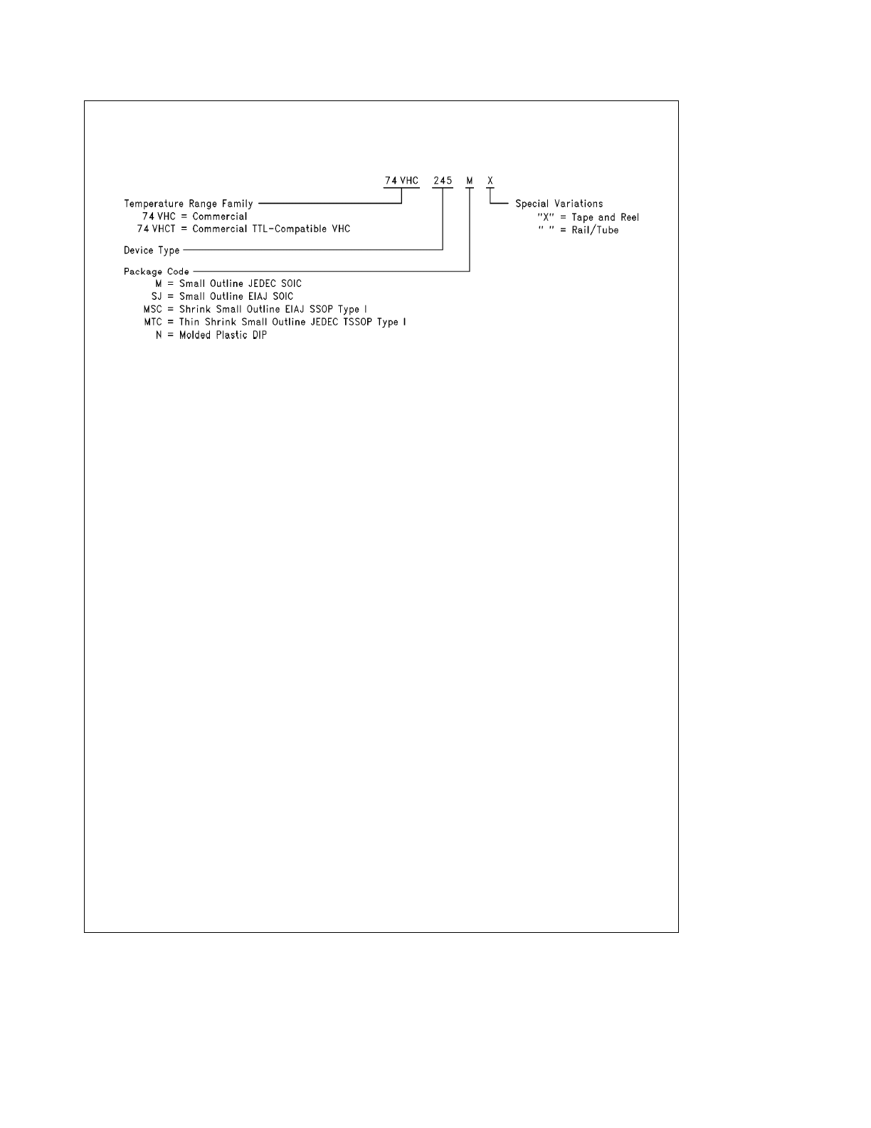
Ordering Information
The device number is used to form part of a simplified purchasing code, where the package type and temperature range are
defined as follows:
TL/F/11520 – 5
6
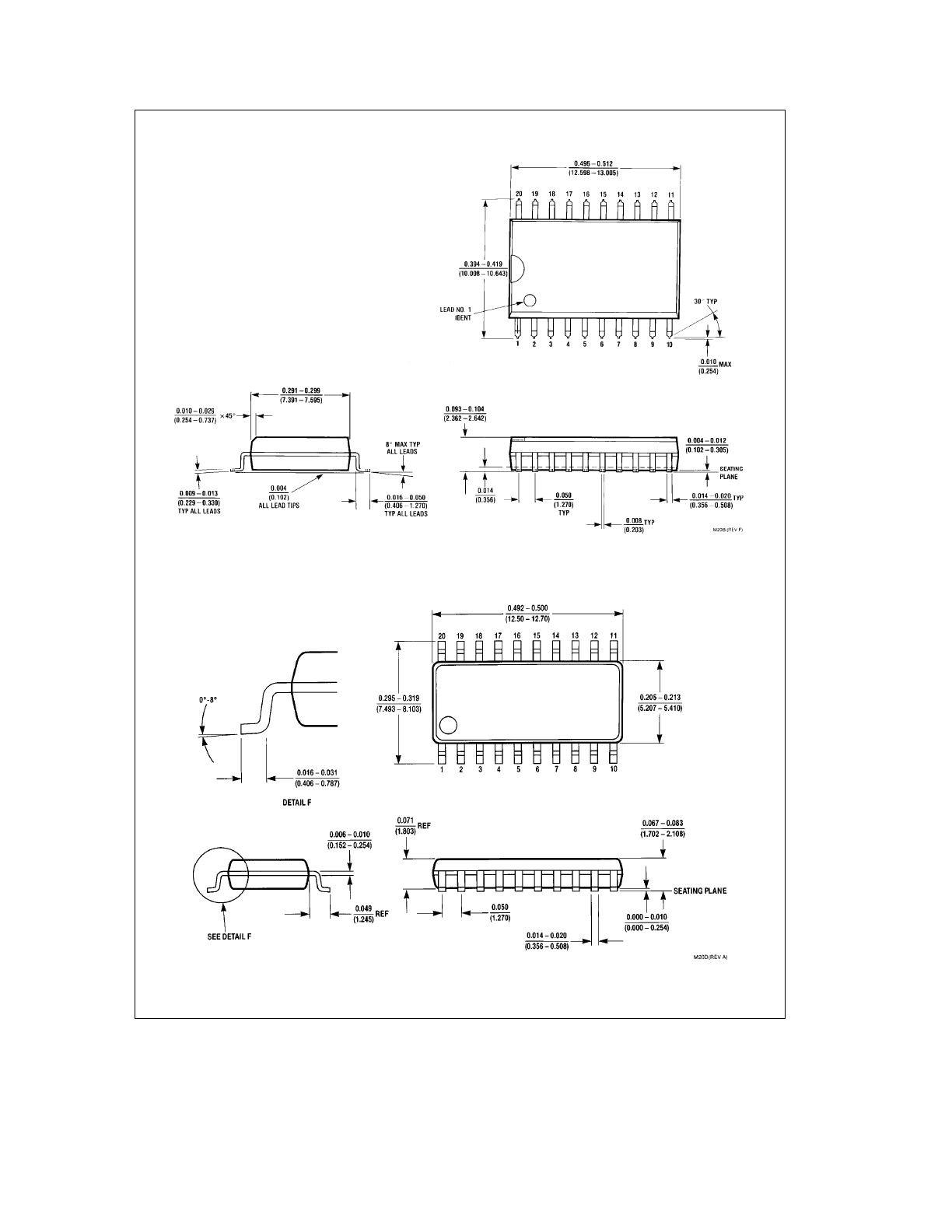
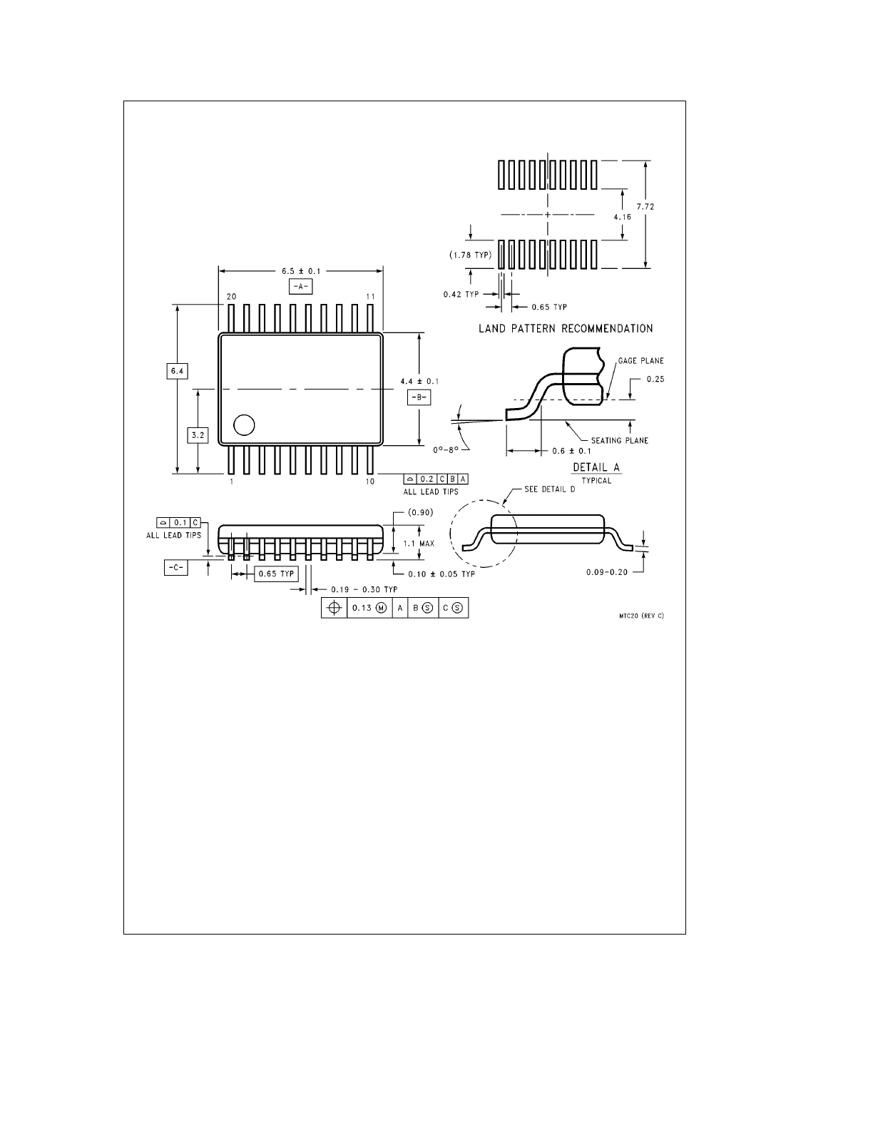
Physical Dimensions
inches (millimeters)
20-Lead Small Outline Integrated CircuitÐJEDEC SOIC (M)
Order Number 74VHC245M, 74VHC245MX, 74VHCT245M, or 74VHCT245MX
NS Package Number M20B
20-Lead Small Outline Package EIAJ SOIC (SJ)
Order Number 74VHC245SJ, 74VHC245SJX, 74VHCT245SJ, or 74VHCT245SJX
NS Package Number M20D
7
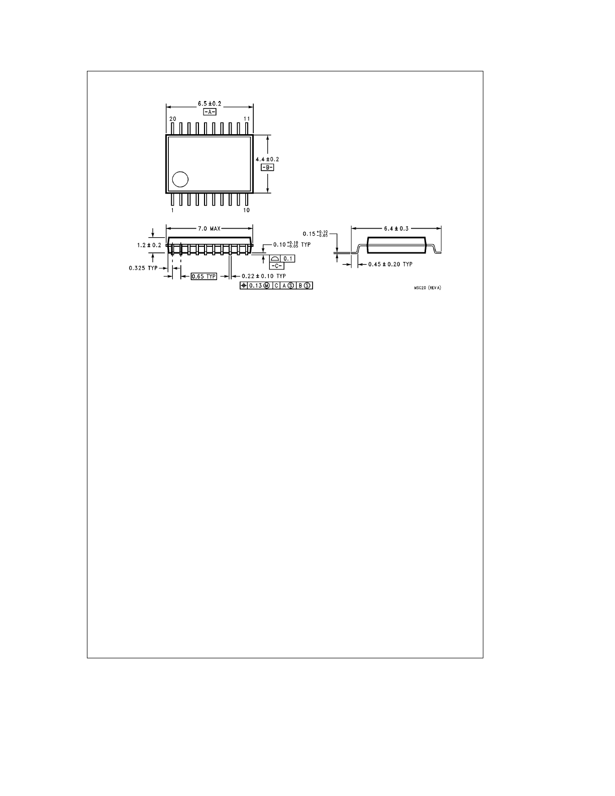
Physical Dimensions
millimeters (Continued)
20-Lead Plastic EIAJ SSOP Type I (MSC)
Order Number 74VHC245MSCX
NS Package Number MSC20
8
Physical Dimensions
millimeters (Continued)
20-Lead Plastic JEDEC TSSOP Type I (MTC)
Order Number 74VHC245MTC, 74VHC245MTCX, 74VHCT245MTC or 74VHCT245MTCX
NS Package Number MTC20
9
74VHC245
#
74VHCT245
Octal
Bidirectional
Transceiver
with
TRI-STATE
Outputs
Physical Dimensions
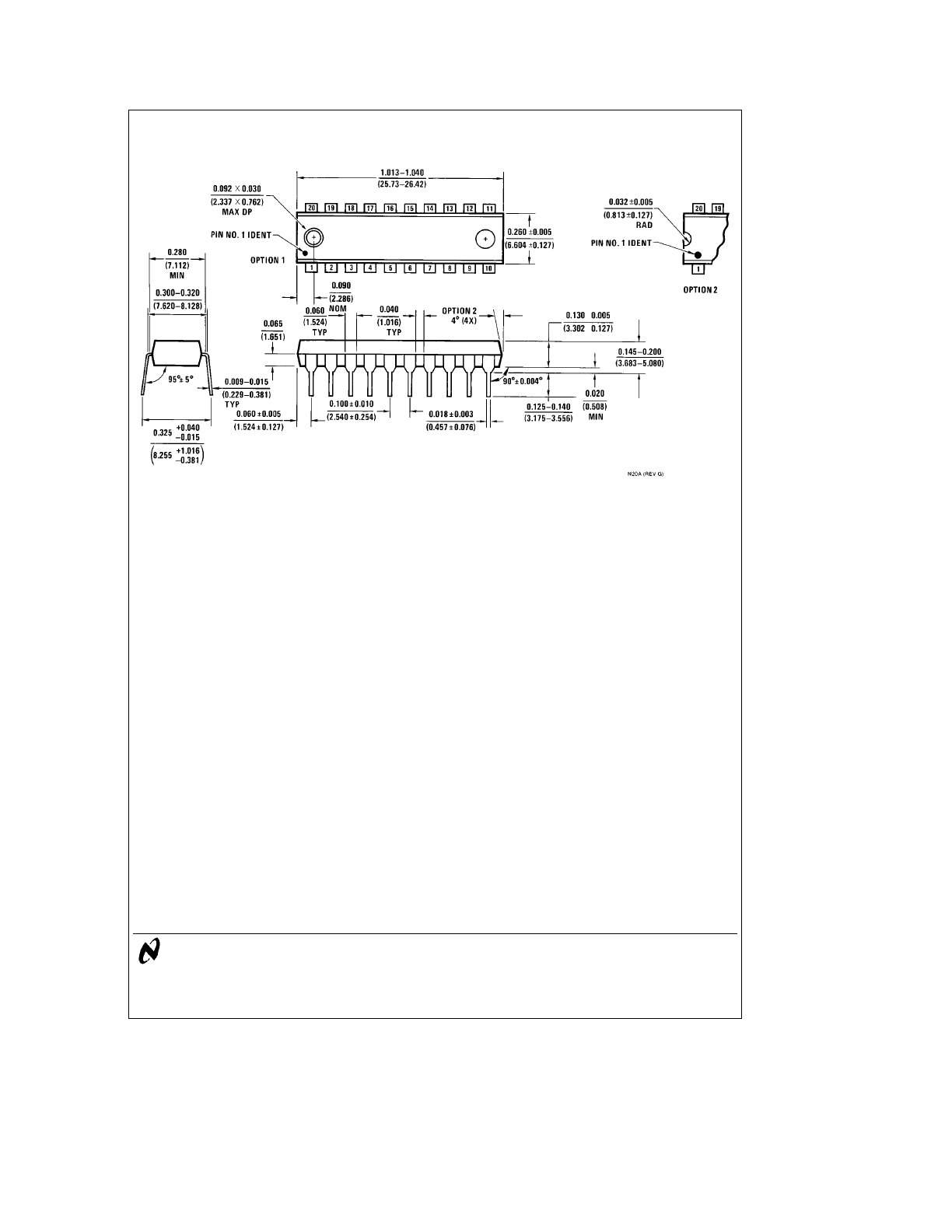
inches (millimeters) (Continued)
20-Lead (0.300
×
Wide) Molded Dual-In-Line Package
Order Number 74VHCT245N
NS Package Number N20A
LIFE SUPPORT POLICY
NATIONAL’S PRODUCTS ARE NOT AUTHORIZED FOR USE AS CRITICAL COMPONENTS IN LIFE SUPPORT
DEVICES OR SYSTEMS WITHOUT THE EXPRESS WRITTEN APPROVAL OF THE PRESIDENT OF NATIONAL
SEMICONDUCTOR CORPORATION. As used herein:
1. Life support devices or systems are devices or
2. A critical component is any component of a life
systems which, (a) are intended for surgical implant
support device or system whose failure to perform can
into the body, or (b) support or sustain life, and whose
be reasonably expected to cause the failure of the life
failure to perform, when properly used in accordance
support device or system, or to affect its safety or
with instructions for use provided in the labeling, can
effectiveness.
be reasonably expected to result in a significant injury
to the user.
National Semiconductor
National Semiconductor
National Semiconductor
National Semiconductor
Corporation
Europe
Hong Kong Ltd.
Japan Ltd.
1111 West Bardin Road
Fax: (
a
49) 0-180-530 85 86
13th Floor, Straight Block,
Tel: 81-043-299-2309
Arlington, TX 76017
Email: cnjwge
@
tevm2.nsc.com
Ocean Centre, 5 Canton Rd.
Fax: 81-043-299-2408
Tel: 1(800) 272-9959
Deutsch Tel: (
a
49) 0-180-530 85 85
Tsimshatsui, Kowloon
Fax: 1(800) 737-7018
English
Tel: (
a
49) 0-180-532 78 32
Hong Kong
Fran
3ais Tel: (
a
49) 0-180-532 93 58
Tel: (852) 2737-1600
Italiano
Tel: (
a
49) 0-180-534 16 80
Fax: (852) 2736-9960
National does not assume any responsibility for use of any circuitry described, no circuit patent licenses are implied and National reserves the right at any time without notice to change said circuitry and specifications.