
TL/F/11504
74VHC00
#
74VHCT00
Quad
2-Input
NAND
Gate
October 1995
74VHC00
#
74VHCT00
Quad 2-Input NAND Gate
General Description
The VHC/VHCT00 is an advanced high-speed CMOS 2-In-
put NAND Gate fabricated with silicon gate CMOS technolo-
gy. It achieves the high-speed operation similar to equiva-
lent Bipolar Schottky TTL while maintaining the CMOS low
power dissipation. The internal circuit is composed of 3
stages, including buffer output, which provide high noise im-
munity and stable output. An input protection circuit insures
that 0V to 7V can be applied to the input pins without regard
to the supply voltage. This device can be used to interface
5V to 3V systems and two supply systems such as battery
backup. This circuit prevents device destruction due to mis-
matched supply and input voltages.
Features
Y
High noise immunity:
VHC
V
NIH
e
V
NIL
e
28% V
CC
(min)
VHCT V
IH
e
2.0V, V
IL
e
0.8V
Y
Power down protection:
VHC
inputs only
VHCT inputs and outputs
Y
Low noise: V
OLP
e
0.8V (max)
Y
Low power dissipation:
I
CC
e
2 mA (max) at T
A
e
25
§
C
Y
Balanced propagation delays: t
PLH
j
t
PHL
Y
Pin and function compatible with 74HC/HCT00
NOTE: ADD EXTERNAL PULL UP RESISTOR TO VHCT
OUTPUTS TO DRIVE CMOS INPUTS
Commercial
Package
Package Description
Number
74VHC00M
M14A
14-Lead Molded JEDEC SOIC
74VHC00SJ
M14D
14-Lead Molded EIAJ SOIC
74VHC00MSC
MSC14
14-Lead Molded EIAJ Type 1 SSOP
74VHC00MTC
MTC14
14-Lead Molded JEDEC Type 1 TSSOP
74VHC00N
N14A
14-Lead Molded DIP
74VHCT00M
M14A
14-Lead Molded JEDEC SOIC
74VHCT00SJ
M14D
14-Lead Molded EIAJ SOIC
74VHCT00MTC
MTC14
14-Lead Molded JEDEC Type 1 TSSOP
74VHCT00N
N14A
14-Lead Molded DIP
Note:
Surface mount packages are also available on Tape and Reel. Specify by appending the suffix letter ‘X’ to the ordering code.
EIAJ Type 1 SSOP available on Tape and Reel only, order MSCX.
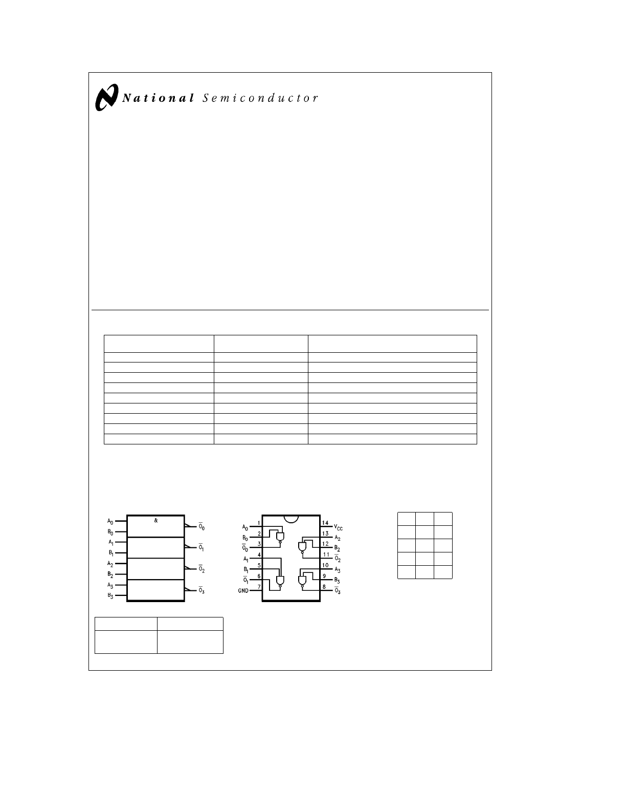
Logic Symbol
IEEE/IEC
TL/F/11504 – 1
Pin Names
Description
An, Bn
Inputs
On
Outputs
Connection Diagram
Pin Assignment for
DIP, SSOP, TSSOP and SOIC
TL/F/11504 – 2
Truth Table
A
B
O
L
L
H
L
H
H
H
L
H
H
H
L
C1995 National Semiconductor Corporation
RRD-B30M125/Printed in U. S. A.
Absolute Maximum Ratings
(Note 1)
Supply Voltage (V
CC
)
b
0.5V to
a
7.0V
DC Input Voltage (V
IN
)
b
0.5V to
a
7.0V
DC Output Voltage (V
OUT
)
VHC
b
0.5V to V
CC
a
0.5V
VHCT*
b
0.5V to 7.0V
Input Diode Current (I
IK
)
b
20 mA
Output Diode Current (I
OK
)
VHC
g
20 mA
VHCT
b
20 mA
DC Output Current (I
OUT
)
g
25 mA
DC V
CC
/GND Current (I
CC
)
g
50 mA
Storage Temperature (T
STG
)
b
65
§
C to
a
150
§
C
Lead Temperature (T
L
)
(Soldering, 10 seconds)
260
§
C
*V
OUT
l
V
CC
only if output is in H state.
Note 1:
Absolute Maximum Ratings are values beyond
which the device may be damaged or have its useful life
impaired. The databook specifications should be met, with-
out exception, to ensure that the system design is reliable
over its power supply, temperature, and output/input load-
ing variables. National does not recommend operation out-
side databook specifications.
Recommended Operating
Conditions
Supply Voltage (V
CC
)
VHC
2.0V to
a
5.5V
VHCT
4.5V to 5.5V
Input Voltage (V
IN
)
0V to
a
5.5V
Output Voltage (V
OUT
)
0V to V
CC
Operating Temperature (T
OPR
)
74VHC/VHCT
b
40
§
C to
a
85
§
C
Input Rise and Fall Time (t
r
, t
f
)
V
CC
e
3.3V
g
0.3V (VHC Only)
0 ns/V E 100 ns/V
V
CC
e
5.0V
g
0.5V
0 ns/V E 20 ns/V
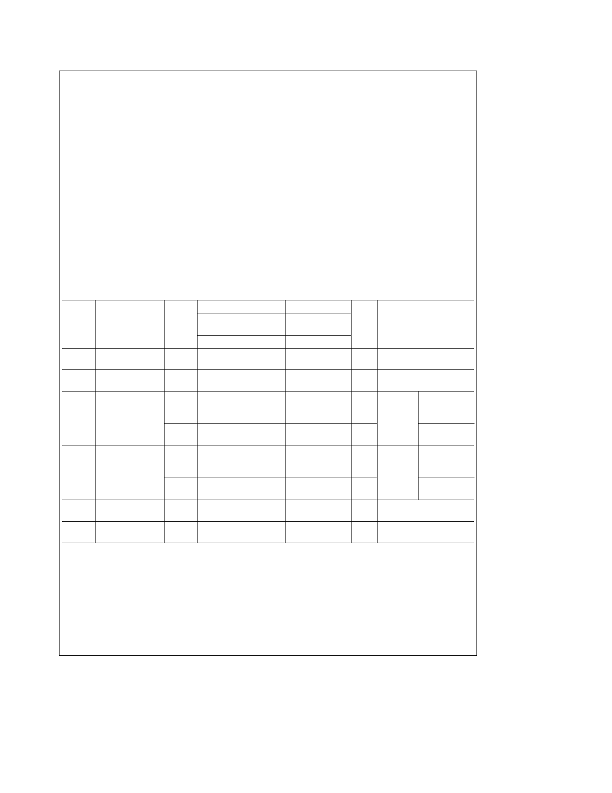
DC Characteristics for ’VHC Family Devices
Symbol
Parameter
V
CC
(V)
74VHC
74VHC
Units
Conditions
T
A
e
25
§
C
T
A
e b
40
§
C
to
a
85
§
C
Min
Typ
Max
Min
Max
V
IH
High Level Input
3.0 – 5.5
2.0
0.7 V
CC
1.50
0.7 V
CC
1.50
V
Voltage
V
IL
Low Level Input
3.0 – 5.5
2.0
0.3 V
CC
0.50
0.3 V
CC
0.50
V
Voltage
V
OH
High Level Output
2.0
1.9
2.0
1.9
V
IN
e
V
IH
I
OH
e b
50 mA
Voltage
3.0
2.9
3.0
2.9
V
or V
IL
4.5
4.4
4.5
4.4
3.0
2.58
2.48
V
I
OH
e b
4 mA
4.5
3.94
3.80
I
OH
e b
8 mA
V
OL
Low Level Output
2.0
0.0
0.1
0.1
V
IN
e
V
IH
I
OL
e
50 mA
Voltage
3.0
0.0
0.1
0.1
V
or V
IL
4.5
0.0
0.1
0.1
3.0
0.36
0.44
V
I
OL
e
4 mA
4.5
0.36
0.50
I
OL
e
8 mA
I
IN
Input Leakage
0 – 5.5
g
0.1
g
1.0
m
A
V
IN
e
5.5V or GND
Current
I
CC
Quiescent Supply
5.5
2.0
20.0
m
A
V
IN
e
V
CC
or GND
Current
2
DC Characteristics for ’VHC Family Devices
Symbol
Parameter
V
CC
(V)
74VHC
Units
Conditions
T
A
e
25
§
C
Typ
Limit
*V
OLP
Quiet Output Maximum
5.0
0.3
0.8
V
C
L
e
50 pF
Dynamic V
OL
*V
OLV
Quiet Output Minimum
5.0
b
0.3
b
0.8
V
C
L
e
50 pF
Dynamic V
OL
*V
IHD
Minimum High Level
5.0
3.5
V
C
L
e
50 pF
Dynamic Input Voltage
*V
ILD
Maximum Low Level
5.0
1.5
V
C
L
e
50 pF
Dynamic Input Voltage
*Parameter guaranteed by design
DC Characteristics for ’VHCT Family Devices
Symbol
Parameter
V
CC
(V)
74VHCT
74VHCT
Units
Conditions
T
A
e
25
§
C
T
A
e b
40
§
C
to
a
85
§
C
Min
Typ
Max
Min
Max
V
IH
High Level Input
4.5
2.0
2.0
V
Voltage
5.5
2.0
2.0
V
IL
Low Level Input
4.5
0.8
0.8
V
Voltage
5.5
0.8
0.8
V
OH
High Level
4.5
3.15
3.65
3.15
V
V
IN
e
V
IH
I
OH
e b
50 mA
Output Voltage
4.5
2.5
2.4
V
I
OH
e b
8 mA
V
OL
Low Level
4.5
0.0
0.1
0.1
V
V
IN
e
V
IH
I
OL
e
50 mA
Output Voltage
4.5
0.36
0.44
V
I
OL
e
8 mA
I
IN
Input Leakage
0 – 5.5
g
0.1
g
1.0
m
A
V
IN
e
5.5V or GND
Current
I
CC
Quiescent
5.5
2.0
20.0
m
A
V
IN
e
V
CC
or GND
Supply Current
I
CCT
Maximum I
CC
/
5.5
1.35
1.50
mA
V
IN
e
3.4V
Input
Other Inputs
e
V
CC
or GND
I
OPD
Output Leakage
0.0
0.5
5.0
m
A
V
OUT
e
5.5V
Current (Power
Down State)
3
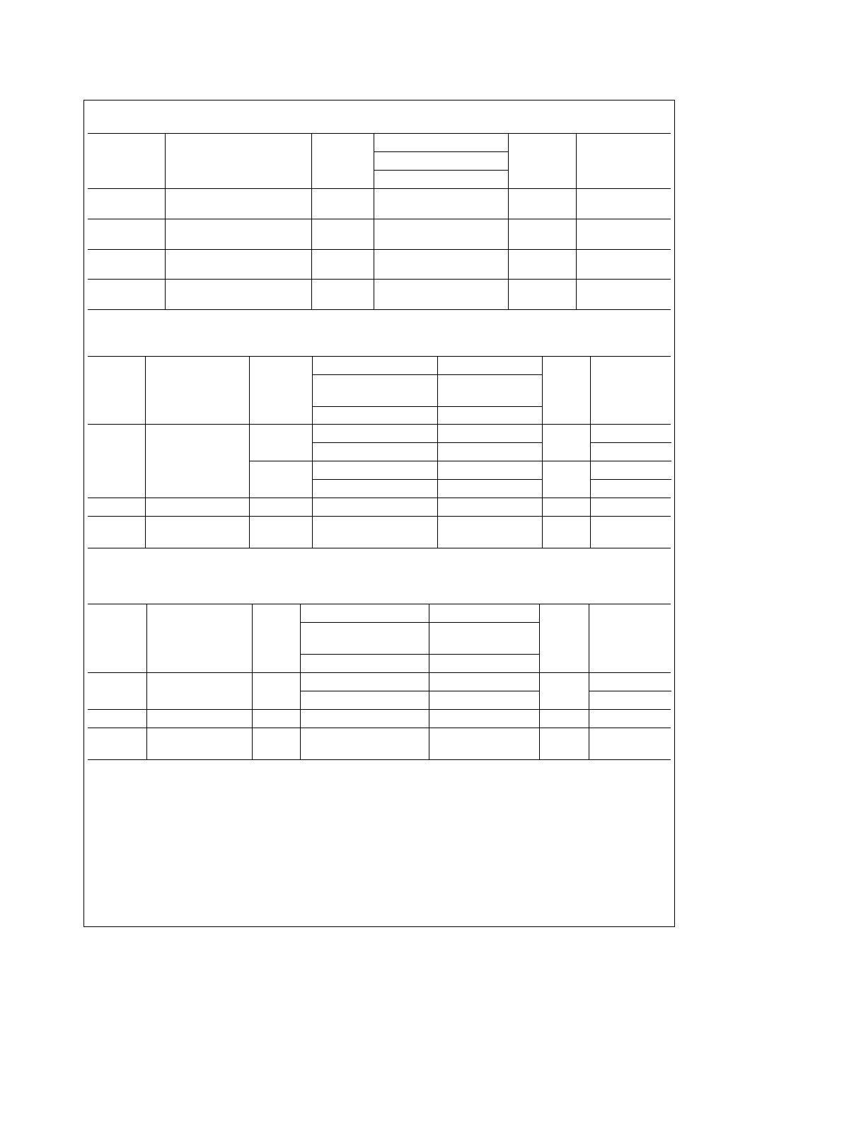
DC Characteristics for ’VHCT Family Devices
Symbol
Parameter
V
CC
(V)
74VHCT
Units
Conditions
T
A
e
25
§
C
Typ
Limit
*V
OLP
Quiet Output Maximum
5.0
0.4
0.8
V
C
L
e
50 pF
Dynamic V
OL
*V
OLV
Quiet Output Minimum
5.0
b
0.4
b
0.8
V
C
L
e
50 pF
Dynamic V
OL
*V
IHD
Minimum High Level
5.0
2.0
V
C
L
e
50 pF
Dynamic Input Voltage
*V
ILD
Maximum Low Level
5.0
0.8
V
C
L
e
50 pF
Dynamic Input Voltage
*Parameter guaranteed by design.
AC Electrical Characteristics for ’VHC Family Devices
Symbol
Parameter
V
CC
(V)
74VHC
74VHC
Units
Conditions
T
A
e
25
§
C
T
A
e b
40
§
C
to
a
85
§
C
Min
Typ
Max
Min
Max
t
PLH
,
Propagation Delay
3.3
g
0.3
5.5
7.9
1.0
9.5
ns
C
L
e
15 pF
t
PHL
8.0
11.4
1.0
13.0
C
L
e
50 pF
5.0
g
0.5
3.7
5.5
1.0
6.5
ns
C
L
e
15 pF
5.2
7.5
1.0
8.5
C
L
e
50 pF
C
IN
Input Capacitance
4
10
10
pF
V
CC
e
Open
C
PD
Power Dissipation
19
pF
(Note 1)
Capacitance
Note 1:
C
PD
is defined as the value of the internal equivalent capacitance which is calculated from the operating current consumption without load. Average
operating current can be obtained from the equation: I
CC
(opr.) e C
PD
* V
CC
* f
IN
a
I
CC
/4 (per gate).
AC Electrical Characteristics for ’VHCT Family Devices
74VHCT
74VHCT
Symbol
Parameter
V
CC
T
A
e
25
§
C
T
A
e b
40
§
C
Units
Conditions
(V)
to
a
85
§
C
Min
Typ
Max
Min
Max
t
PLH
,
Propagation Delay
5.0
5.0
6.9
1.0
8.0
ns
C
L
e
15 pF
t
PHL
g
0.5
5.5
7.9
1.0
9.0
C
L
e
50 pF
C
IN
Input Capacitance
4
10
10
pF
V
CC
e
Open
C
PD
Power Dissipation
17
pF
(Note 1)
Capacitance
Note 1:
C
PD
is defined as the value of the internal equivalent capacitance, which is calculated from the operating current consumption without load. Average
operating current can be obtained from the equation: I
CC
(opr.) e C
PD
* V
CC
* f
IN
a
I
CC
/4 (per gate)
4
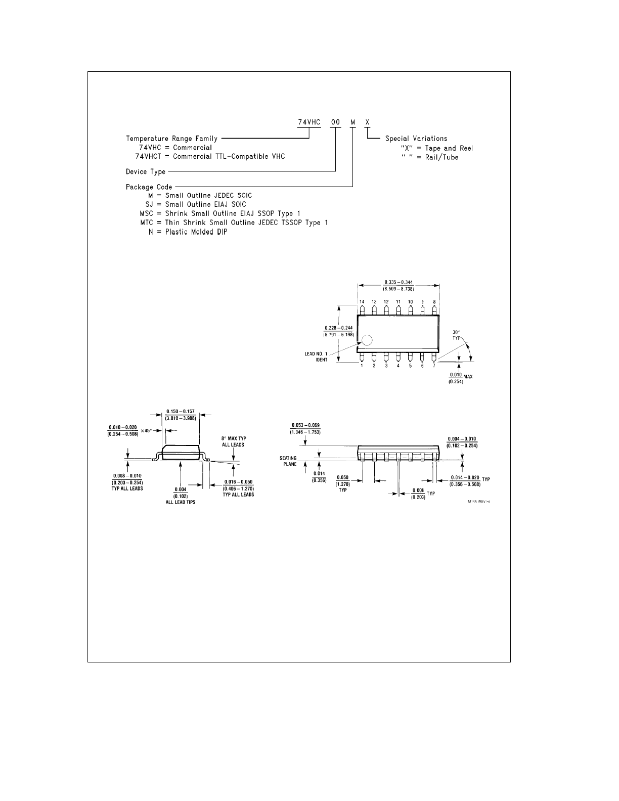
Ordering Information
The device number is used to form part of a simplified purchasing code, where the package type and temperature range are
defined as follows:
TL/F/11504 – 4
Physical Dimensions
inches (millimeters)
14-Lead Small Outline Integrated CircuitÐJEDEC (M)
Order Number 74VHC00M, 74VHC00MX, 74VHCT00M or 74VHCT00MX
NS Package Number M14A
5
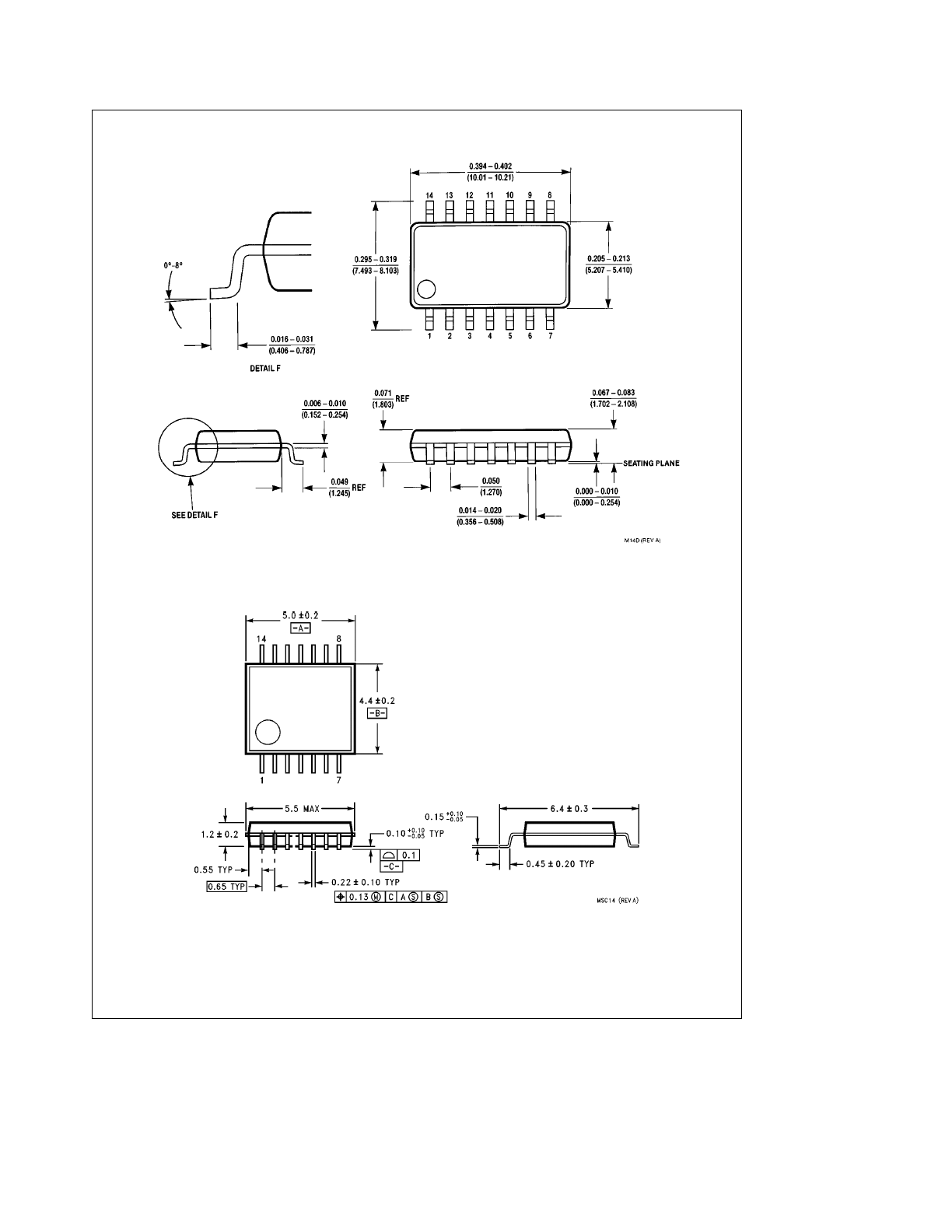
Physical Dimensions
inches (millimeters) (Continued)
14-Lead Plastic EIAJ SOIC (SJ)
Order Number 74VHC00SJ, 74VHC00SJX, 74VHCT00SJ or 74VHCT00SJX
NS Package Number M14D
14-Lead Plastic EIAJ SSOP Type I (MSC)
Order Number 74VHC00MSCX
NS Package Number MSC14
6
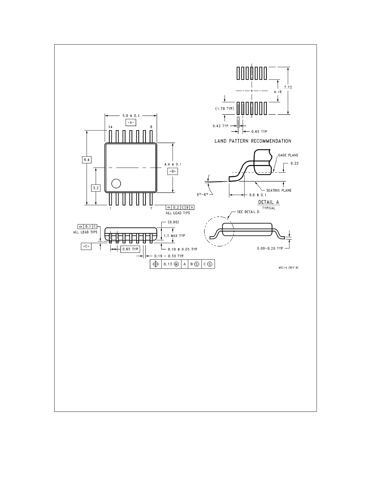
Physical Dimensions
inches (millimeters) (Continued)
14-Lead Plastic JEDEC TSSOP Type 1 (MTC)
Order Number 74VHC00MTC, 74VHC00MTCX, 74VHCT00MTC or 74VHCT00MTCX
NS Package Number MTC14
7
74VHC00
#
74VHCT00
Quad
2-Input
NAND
Gate
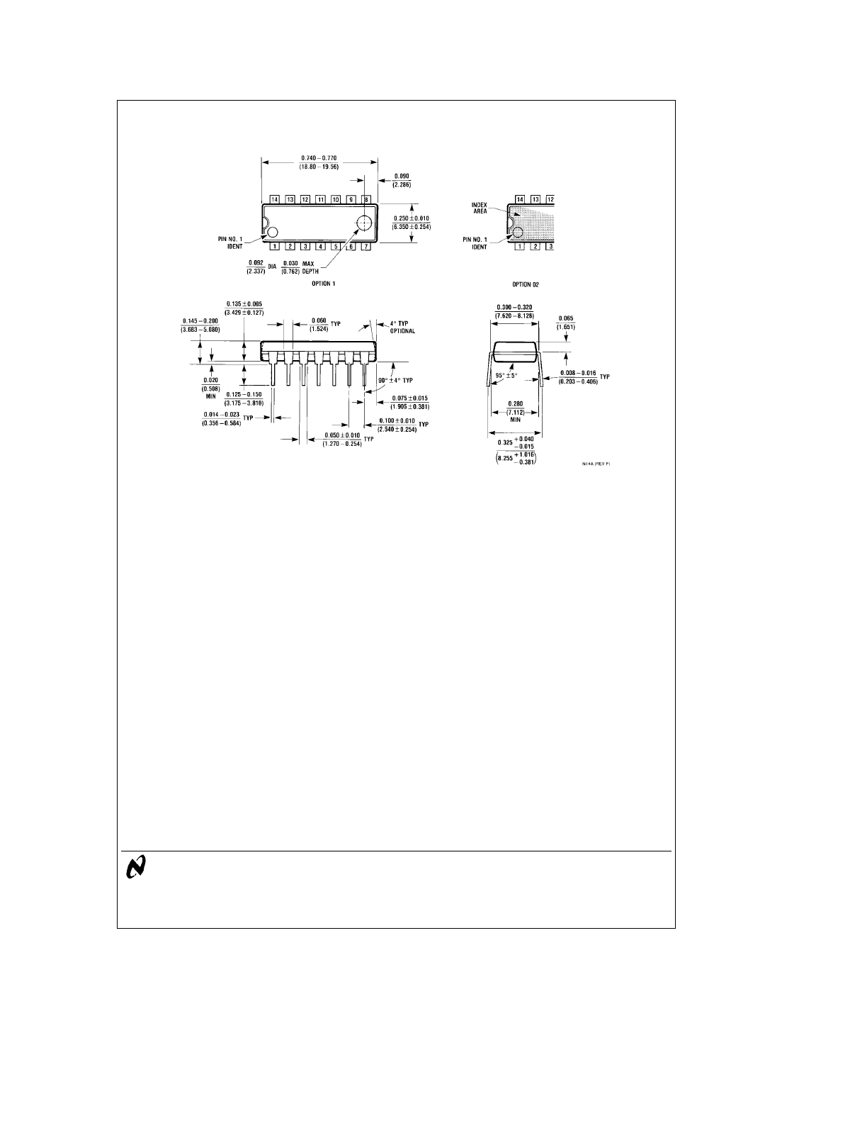
Physical Dimensions
inches (millimeters) (Continued)
14-Lead Molded DIP (P)
Order Number 74VHC00N or 74VHCT00N
NS Package Number N14A
LIFE SUPPORT POLICY
NATIONAL’S PRODUCTS ARE NOT AUTHORIZED FOR USE AS CRITICAL COMPONENTS IN LIFE SUPPORT
DEVICES OR SYSTEMS WITHOUT THE EXPRESS WRITTEN APPROVAL OF THE PRESIDENT OF NATIONAL
SEMICONDUCTOR CORPORATION. As used herein:
1. Life support devices or systems are devices or
2. A critical component is any component of a life
systems which, (a) are intended for surgical implant
support device or system whose failure to perform can
into the body, or (b) support or sustain life, and whose
be reasonably expected to cause the failure of the life
failure to perform, when properly used in accordance
support device or system, or to affect its safety or
with instructions for use provided in the labeling, can
effectiveness.
be reasonably expected to result in a significant injury
to the user.
National Semiconductor
National Semiconductor
National Semiconductor
National Semiconductor
Corporation
Europe
Hong Kong Ltd.
Japan Ltd.
1111 West Bardin Road
Fax: (
a
49) 0-180-530 85 86
13th Floor, Straight Block,
Tel: 81-043-299-2309
Arlington, TX 76017
Email: cnjwge
@
tevm2.nsc.com
Ocean Centre, 5 Canton Rd.
Fax: 81-043-299-2408
Tel: 1(800) 272-9959
Deutsch Tel: (
a
49) 0-180-530 85 85
Tsimshatsui, Kowloon
Fax: 1(800) 737-7018
English
Tel: (
a
49) 0-180-532 78 32
Hong Kong
Fran
3ais Tel: (
a
49) 0-180-532 93 58
Tel: (852) 2737-1600
Italiano
Tel: (
a
49) 0-180-534 16 80
Fax: (852) 2736-9960
National does not assume any responsibility for use of any circuitry described, no circuit patent licenses are implied and National reserves the right at any time without notice to change said circuitry and specifications.