
TL/F/11540
74LVX4245
8-Bit
Dual
Supply
Translating
Transceiver
with
TRI-STATE
Outputs
October 1995
74LVX4245
8-Bit Dual Supply Translating Transceiver
with TRI-STATE
É
Outputs
General Description
The LVX4245 is a dual-supply, 8-bit translating transceiver
that is designed to interface between a 5V bus and a 3V bus
in a mixed 3V/5V supply environment. The Transmit/Re-
ceive (T/R) input determines the direction of data flow.
Transmit (active-HIGH) enables data from A ports to B
ports; Receive (active-LOW) enables data from B ports to A
ports. The Output Enable input, when HIGH, disables both A
and B ports by placing them in a HIGH Z condition. The A
port interfaces with the 5V bus; the B port interfaces with
the 3V bus.
The LVX4245 is suitable for mixed voltage applications such
as laptop computers using 3.3V CPU’s and 5V LCD dis-
plays.
Features
Y
Bidirectional interface between 5V and 3V buses
Y
Control inputs compatible with TTL level
Y
5V data flow at A port and 3V data flow at B port
Y
Outputs source/sink 24 mA at 5V bus; 12 mA at 3V
bus
Y
Guaranteed simultaneous switching noise level and dy-
namic threshold performance
Y
Available in SOIC, QSOP and TSSOP packages
Y
Implements patented Quiet Series EMI reduction
circuitry
Y
Functionally compatible with the 74 series 245
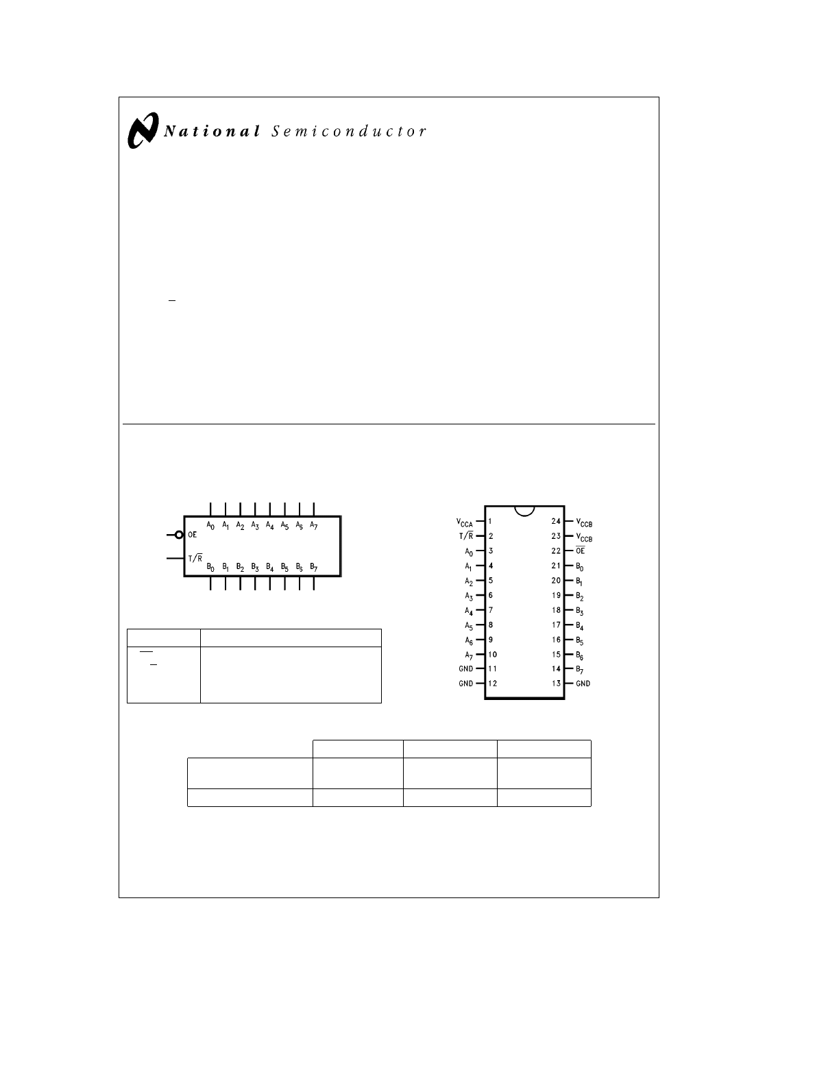
Logic Symbol
TL/F/11540 – 1
Pin Names
Description
OE
Output Enable Input
T/R
Transmit/Receive Input
A
0
– A
7
Side A Inputs or TRI-STATE Outputs
B
0
– B
7
Side B Inputs or TRI-STATE Outputs
Connection Diagram
Pin Assignment
for SOIC, QSOP and TSSOP
TL/F/11540 – 2
SOIC JEDEC
QSOP
TSSOP
Order Number
74LVX4245WM
74LVX4245QSC
74LVX4245MTC
74LVX4245WMX
74LVX4245QSCX
74LVX4245MTCX
See NS Package Number
M24B
MQA24
MTC24
TRI-STATE
É
is a registered trademark of National Semiconductor Corporation.
C1995 National Semiconductor Corporation
RRD-B30M115/Printed in U. S. A.
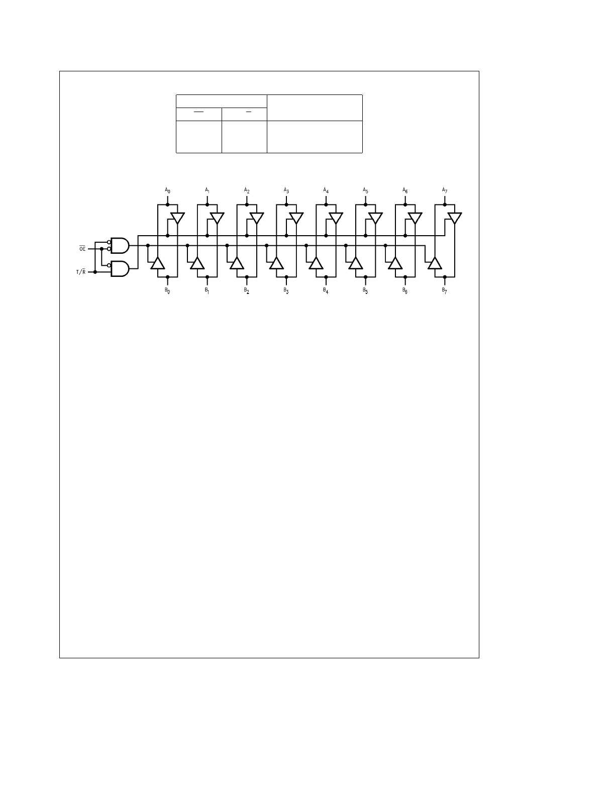
Truth Table
Inputs
Outputs
OE
T/R
L
L
Bus B Data to Bus A
L
H
Bus A Data to Bus B
H
X
HIGH-Z State
Logic Diagram
TL/F/11540 – 6
2
Absolute Maximum Ratings
(Note)
If Military/Aerospace specified devices are required,
please contact the National Semiconductor Sales
Office/Distributors for availability and specifications.
Supply Voltage (V
CCA
, V
CCB
)
b
0.5V to
a
7.0V
DC Input Voltage (V
I
)
@
OE, T/R
b
0.5V to V
CCA
a
0.5V
DC Input/Output Voltage (V
I/O
)
@
A(n)
b
0.5V to V
CCA
a
0.5V
@
B(n)
b
0.5V to V
CCB
a
0.5V
DC Input Diode Current (I
IN
)
@
OE, T/R
g
20 mA
DC Output Diode Current (I
OK
)
g
50 mA
DC Output Source or Sink Current (I
O
)
g
50 mA
DC V
CC
or Ground Current
per Output Pin (I
CC
or I
GND
)
g
50 mA
and Max Current
@
I
CCA
g
200 mA
@
I
CCB
g
100 mA
Storage Temperature Range (T
STG
)
b
65
§
C to
a
150
§
C
DC Latch-Up Source or Sink Current
g
300 mA
Note:
The ‘‘Absolute Maximum Ratings’’ are those values
beyond which the safety of the device cannot be guaran-
teed. The device should not be operated at these limits. The
parametric values defined in the ‘‘Electrical Characteristics’’
table are not guaranteed at the absolute maximum ratings.
The ‘‘Recommended Operating Conditions’’ table will define
the conditions for actual device operation
.
Recommended Operating
Conditions
Supply Voltage
V
CCA
4.5V to 5.5V
V
CCB
2.7V to 3.6V
Input Voltage (V
I
)
@
OE, T/R
0V to V
CCA
Input/Output Voltage (V
I/O
)
@
A(n)
0V to V
CCA
@
B(n)
0V to V
CCB
Free Air Operating Temperature (T
A
)
74LVX
b
40
§
C to
a
85
§
C
Minimum Input Edge Rate (Dt/DV)
8 ns/V
V
IN
from 30% to 70% of V
CC
V
CC
@
3.0V, 4.5V, 5.5V
DC Electrical Characteristics
Symbol
Parameter
V
CCA
(V)
V
CCB
(V)
74LVX4245
74LVX4245
Units
Conditions
T
A
a
25
§
C
T
A
e b
40
§
C
to
a
85
§
C
Typ
Guaranteed Limits
V
IHA
Minimum
A(n), T/R,
5.5
3.3
2.0
2.0
V
V
OUT
s
0.1V or
High Level
OE
4.5
3.3
2.0
2.0
t
V
CC
b
0.1V
V
IHB
Input Voltage
B(n)
5.0
3.6
2.0
2.0
5.0
2.7
2.0
2.0
V
ILA
Maximum Low Level
A(n), T/R,
5.5
3.3
0.8
0.8
V
V
OUT
s
0.1V or
Input Voltage
OE
4.5
3.3
0.8
0.8
t
V
CC
b
0.1V
V
ILB
B(n)
5.0
2.7
0.8
0.8
5.0
3.6
0.8
0.8
V
OHA
Minimum High Level
4.5
3.0
4.5
4.4
4.4
V
I
OUT
e b
100 mA
Output Voltage
4.5
3.0
4.25
3.86
3.76
I
OH
e b
24 mA
V
OHB
4.5
3.0
2.99
2.9
2.9
V
I
OUT
e b
100 mA
4.5
3.0
2.8
2.4
2.4
I
OH
e b
12 mA
4.5
2.7
2.5
2.4
2.4
I
OL
e b
8 mA
V
OLA
Maximum Low Level
4.5
3.0
0.002
0.1
0.1
V
I
OUT
e
100 mA
Output Voltage
4.5
3.0
0.18
0.36
0.44
I
OL
e
24 mA
V
OLB
4.5
3.0
0.002
0.1
0.1
I
OUT
e
100 mA
4.5
3.0
0.1
0.31
0.4
V
I
OL
e
12 mA
4.5
2.7
0.1
0.31
0.4
I
OL
e
8 mA
I
IN
Maximum Input
V
I
e
V
CCA
, GND
Leakage Current
5.5
3.6
g
0.1
g
1.0
m
A
@
OE, T/R
I
OZA
Maximum TRI-STATE
V
I
e
V
IL
, V
IH
Output Leakage
5.5
3.6
g
0.5
g
5.0
m
A
OE
e
V
CCA
@
A(n)
V
O
e
V
CCA
, GND
3
DC Electrical Characteristics
(Continued)
Symbol
Parameter
V
CCA
(V)
V
CCB
(V)
74LVX4245
74LVX4245
Units
Conditions
T
A
e a
25
§
C
T
A
e b
40
§
C
to
a
85
§
C
Typ
Guaranteed Limits
I
OZB
Maximum TRI-STATE
V
I
e
V
IL
, V
IH
Output Leakage
5.5
3.6
g
0.5
g
5.0
m
A
OE
e
V
CCA
@
B(n)
V
O
e
V
CCB
, GND
D
I
CC
Maximum I
CCT
/Input
5.5
3.6
1.0
1.35
1.5
mA
V
I
e
V
CCA
b
2.1V
@
A(n), T/R, OE
Input
@
B(n)
5.5
3.6
0.35
0.5
mA
V
I
e
V
CCB
b
0.6V
I
CCA
Quiescent V
CCA
A(n)
e
V
CCA
or GND
Supply Current
5.5
3.6
8
80
m
A
B(n)
e
V
CCB
or GND,
OE
e
GND T/R
e
GND
I
CCB
Quiescent V
CCB
A(n)
e
V
CCA
or GND
Supply Current
5.5
3.6
5
50
m
A
B(n)
e
V
CCB
or GND,
OE
e
GND T/R
e
V
CCA
V
OLPA
Quiet Output Maximum
5.0
3.3
1.5
V
(Notes 1, 2)
V
OLPB
Dynamic V
OL
5.0
3.3
0.8
V
OLVA
Quiet Output Minimum
5.0
3.3
b
1.2
V
(Notes 1, 2)
V
OLVB
Dynamic V
OL
5.0
3.3
b
0.8
V
IHDA
Minimum High Level
5.0
3.3
2.0
V
(Notes 1, 3)
V
IHDB
Dynamic Input Voltage
5.0
3.3
2.0
V
ILDA
Maximum Low Level
5.0
3.3
0.8
V
(Notes 1, 3)
V
ILDB
Dynamic Input Voltage
5.0
3.3
0.8
²Maximum test duration 2.0 ms, one output loaded at a time.
Note 1:
Worst case package.
Note 2:
Max number of outputs defined as (n). Data inputs are driven 0V to V
CC
level; one output at GND.
Note 3:
Max number of Data Inputs (n) switching. (nb1) inputs switching 0V to V
CC
level. Input-under-test switching: V
CC
level to threshold (V
IHD
), OV to threshold
(V
ILD
), f e 1 MHz.
4
AC Electrical Characteristics
Symbol
Parameters
74LVX4245
74LVX4245
74LVX4245
Units
T
A
e a
25
§
C
T
A
e b
40
§
C to
a
85
§
C
T
A
e b
40
§
C to
a
85
§
C
C
L
e
50 pF
C
L
e
50 pF
C
L
e
50 pF
*V
CCA
e
5V
*V
CCA
e
5V
*V
CCA
e
5V
**V
CCB
e
3.3V
**V
CCB
e
3.3V
V
CCB
e
2.7V
Min
Typ
Max
Min
Max
Min
Max
t
PHL
Propagation Delay
1.0
5.1
8.5
1.0
9.0
1.0
10.0
ns
t
PLH
A to B
1.0
5.3
8.5
1.0
9.0
1.0
10.0
t
PHL
Propagation Delay
1.0
5.4
8.5
1.0
9.0
1.0
10.0
ns
t
PLH
B to A
1.0
5.5
8.5
1.0
9.0
1.0
10.0
t
PZL
Output Enable Time
1.0
6.5
10.0
1.0
10.5
1.0
11.5
ns
t
PZH
OE to B
1.0
6.7
10.0
1.0
10.5
1.0
11.5
t
PZL
Output Enable Time
1.0
5.2
9.0
1.0
9.5
1.0
10.0
ns
t
PZH
OE to A
1.0
5.8
9.0
1.0
9.5
1.0
10.0
t
PHZ
Output Disable Time
1.0
6.0
9.5
1.0
10.0
1.0
10.0
ns
t
PLZ
OE to B
1.0
3.3
6.5
1.0
7.0
1.0
7.5
t
PHZ
Output Disable Time
1.0
3.9
7.0
1.0
7.5
1.0
7.5
ns
t
PLZ
OE to A
1.0
2.9
6.5
1.0
7.0
1.0
7.5
t
OSHL
Output to Output
t
OSLH
Skew***
1.0
1.5
1.5
1.5
ns
Data to Output
*Voltage Range 5.0V is 5.0V
g
0.5V.
**Voltage Range 3.3V is 3.3V
g
0.3V.
***Skew is defined as the absolute value of the difference between the actual propagation delay for any two separate outputs of the same device. The
specification applies to any outputs switching in the same direction, either HIGH to LOW (t
OSHL
) or LOW to HIGH (t
OSLH
). Parameter guaranteed by
design.
Capacitance
Symbol
Parameter
Typ
Units
Conditions
C
IN
Input Capacitance
4.5
pF
V
CC
e
Open
C
I/O
Input/Output
15
pF
V
CCA
e
5.0V
Capacitance
V
CCB
e
3.3V
C
PD
Power Dissipation
B
x
A
55
pF
V
CCA
e
5.0V
Capacitance
A
x
B
40
pF
V
CCB
e
3.3V
C
PD
is measured at 10 MHz
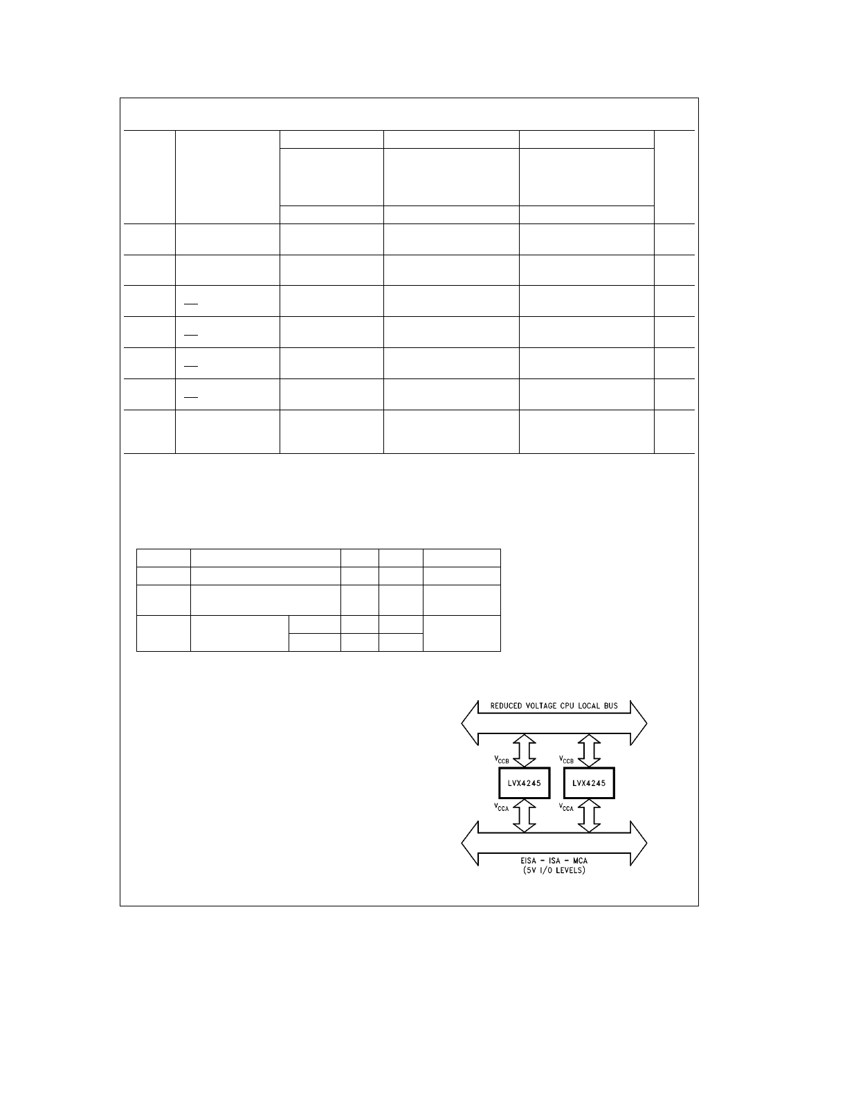
8-Bit Dual Supply Translating Transceiver
The LVX4245 is a dual supply device capable of bidirection-
al signal translation. This level shifting ability provides an
efficient interface between low voltage CPU local bus with
memory and a standard bus defined by 5V I/O levels. The
device control inputs can be controlled by either the low
voltage CPU and core logic or a bus arbitrator with 5V I/O
levels.
Manufactured on a sub-micron CMOS process, the
LVX4245 is ideal for mixed voltage applications such as
notebook computers using 3.3V CPU’s and 5V peripheral
devices.
TL/F/11540 – 3
5
Applications: Mixed Mode Dual Supply Interface Solution
LVX4245 is designed to solve 3V/5V interfacing issues
when CMOS devices cannot tolerate I/O levels above their
applied V
CC
. If an I/O pin of 3V ICs is driven by 5V ICs, the
P-Channel transistor in 3V ICs will conduct causing current
flow from I/O bus to the 3V power supply. The resulting high
current flow can cause destruction of 3V ICs through latch-
up effects. To prevent this problem, a current limiting resis-
tor is used typically under direct connection of 3V ICs and
5V ICs, but it causes speed degradation.
In a better solution, the LVX4245 configures two different
output levels to handle the dual supply interface issues. The
‘‘A’’ port is a dedicated 5V port to interface 5V ICs. The ‘‘B’’
port is a dedicated port to interface 3V ICs.
Figure 1
shows
how LVX4245 fits into a system with 3V subsystem and 5V
subsystem.
This device is also configured as an 8-bit 245 transceiver,
giving the designer TRI-STATE capabilities and the ability to
select either bidirectional or unidirectional modes. Since the
center 20 pins are also pin compatible to 74 series 245, as
shown in
Figure 2
, the designer could use this device in
either a 3V system or a 5V system without any further work
to re-layout the board.
TL/F/11540 – 4
FIGURE 2. LVX4245 Pin Arrangment is Compatible to
20-Pin 74 Series 245
TL/F/11540 – 5
FIGURE 1. LVX4245 Fits into a System with 3V Subsystem and 5V Subsystem
6
74LVX4245 Ordering Information
The device number is used to form part of a simplified purchasing code where the package type and temperature range are
defined as follows:
74LVX
4245
MW
X
Temperature Range Family
Special Variations
74
e
Commercial
‘‘X’’
e
Tape and Reel
‘‘ ’’
e
Rail/Tube
Device Type
Package Code
WM
e
Small Outline JEDEC
SOIC (0.300
×
Wide)
QSC
e
Molded Shrink Small Outline Package, JEDEC
(also known as QSOP)
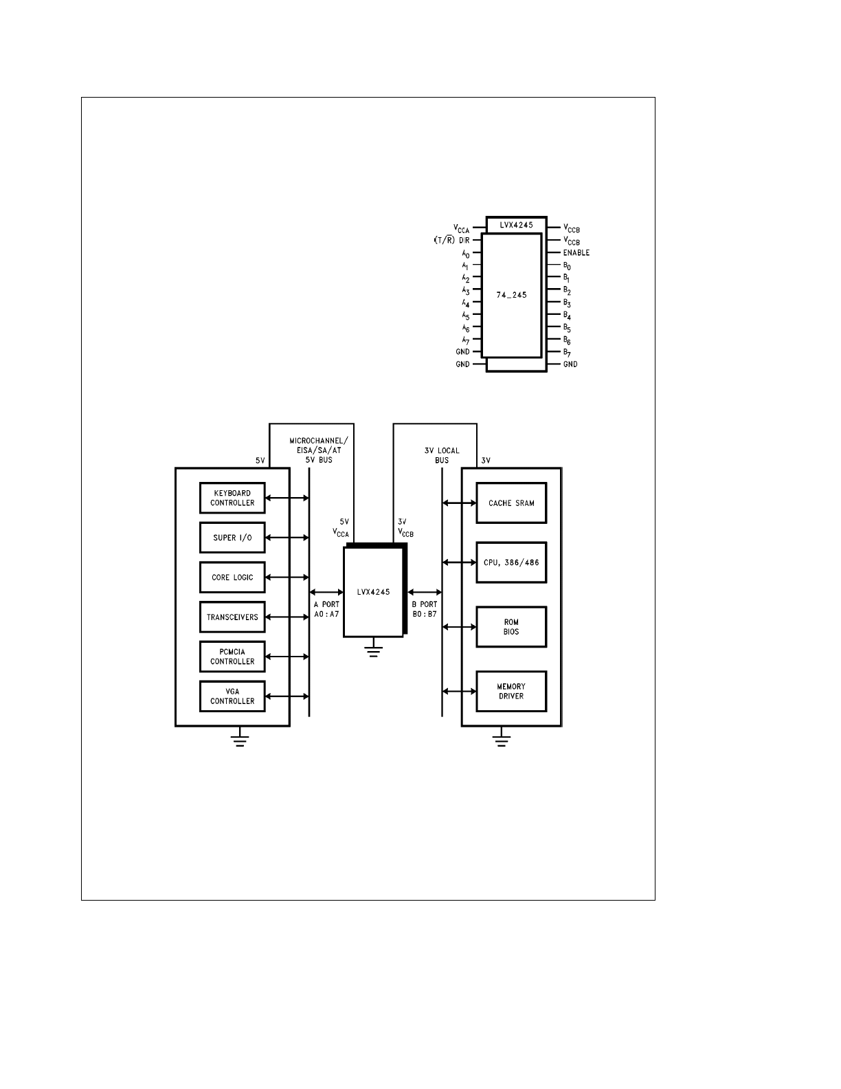
Physical Dimensions
inches
millimeters
24-Lead (0.300
×
Wide) Small Outline Package (WM)
Order Number 74LVX4245WM or 74LVX4245WMX
NS Package Number M24B
7
74LVX4245
8-Bit
Dual
Supply
Translating
Transceiver
with
TRI-STATE
Outputs
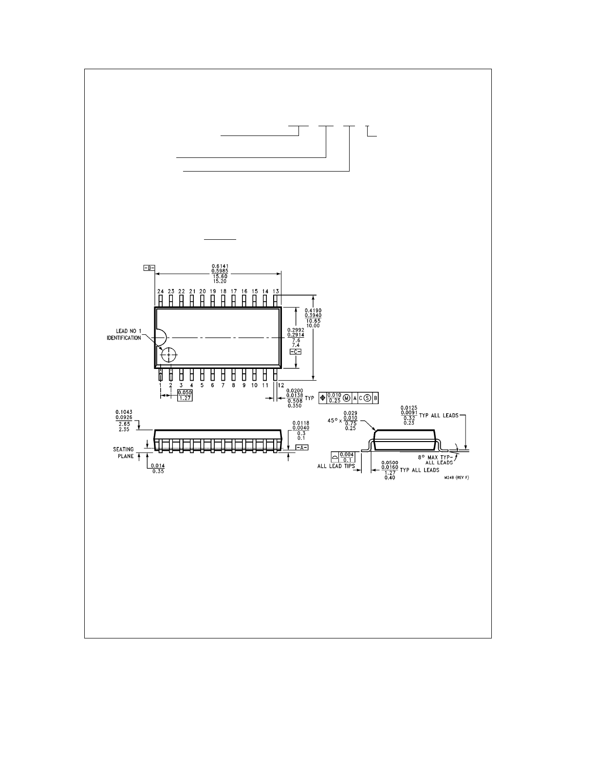
Physical Dimensions
inches (Continued)
24-Lead, Molded Shrink Small Outline Package, JEDEC (QSC)
(also known as: QSOP)
Order Number 74LVX4245QSC or 74LVX4245QSCX
NS Package Number MQA24
LIFE SUPPORT POLICY
NATIONAL’S PRODUCTS ARE NOT AUTHORIZED FOR USE AS CRITICAL COMPONENTS IN LIFE SUPPORT
DEVICES OR SYSTEMS WITHOUT THE EXPRESS WRITTEN APPROVAL OF THE PRESIDENT OF NATIONAL
SEMICONDUCTOR CORPORATION. As used herein:
1. Life support devices or systems are devices or
2. A critical component is any component of a life
systems which, (a) are intended for surgical implant
support device or system whose failure to perform can
into the body, or (b) support or sustain life, and whose
be reasonably expected to cause the failure of the life
failure to perform, when properly used in accordance
support device or system, or to affect its safety or
with instructions for use provided in the labeling, can
effectiveness.
be reasonably expected to result in a significant injury
to the user.
National Semiconductor
National Semiconductor
National Semiconductor
National Semiconductor
Corporation
Europe
Hong Kong Ltd.
Japan Ltd.
1111 West Bardin Road
Fax: (
a
49) 0-180-530 85 86
13th Floor, Straight Block,
Tel: 81-043-299-2309
Arlington, TX 76017
Email: cnjwge
@
tevm2.nsc.com
Ocean Centre, 5 Canton Rd.
Fax: 81-043-299-2408
Tel: 1(800) 272-9959
Deutsch Tel: (
a
49) 0-180-530 85 85
Tsimshatsui, Kowloon
Fax: 1(800) 737-7018
English
Tel: (
a
49) 0-180-532 78 32
Hong Kong
Fran
3ais Tel: (
a
49) 0-180-532 93 58
Tel: (852) 2737-1600
Italiano
Tel: (
a
49) 0-180-534 16 80
Fax: (852) 2736-9960
National does not assume any responsibility for use of any circuitry described, no circuit patent licenses are implied and National reserves the right at any time without notice to change said circuitry and specifications.