
Order this document
by MC74LCX245/D
SEMICONDUCTOR TECHNICAL DATA
1
REV 3
Motorola, Inc. 1995
9/95
!(!% %
# $'#
% !# % "&%$ &%"&%$
%% ! '#%
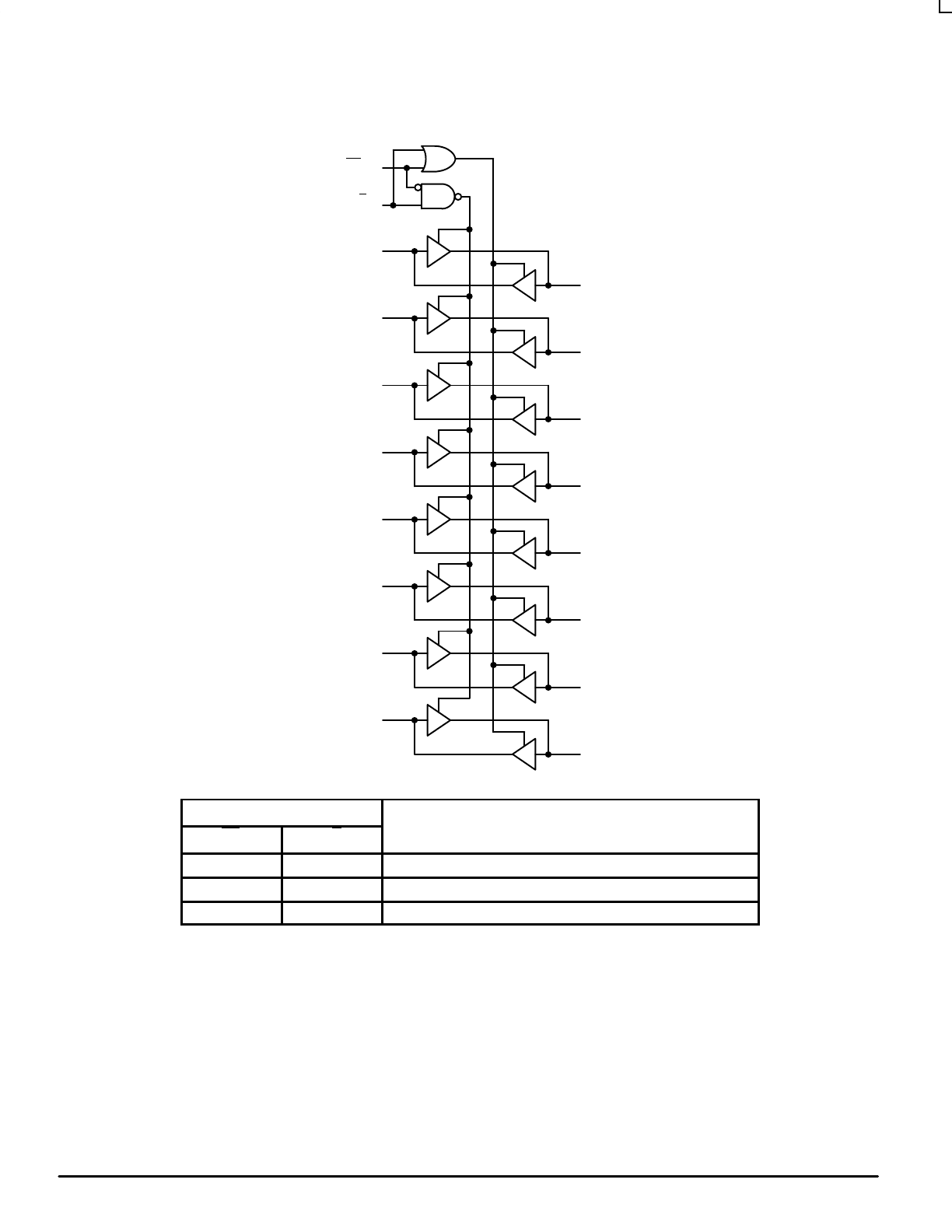
The MC74LCX245 is a high performance, non–inverting octal
transceiver operating from a 2.7 to 3.6V supply. High impedance TTL
compatible inputs significantly reduce current loading to input drivers
while TTL compatible outputs offer improved switching noise
performance. A VI specification of 5.5V allows MC74LCX245 inputs to be
safely driven from 5V devices. The MC74LCX245 is suitable for memory
address driving and all TTL level bus oriented transceiver applications.
Current drive capability is 24mA at both A and B ports. The
Transmit/Receive (T/R) input determines the direction of data flow
through the bi–directional transceiver. Transmit (active–HIGH) enables
data from A ports to B ports; Receive (active–LOW) enables data from B
to A ports. The Output Enable input, when HIGH, disables both A and B
ports by placing them in a HIGH Z condition.
•
Designed for 2.7 to 3.6V VCC Operation
•
5V Tolerant — Interface Capability With 5V TTL Logic
•
Supports Live Insertion and Withdrawal
•
IOFF Specification Guarantees High Impedance When VCC = 0V
•
LVTTL Compatible
•
LVCMOS Compatible
•
24mA Balanced Output Sink and Source Capability
•
Near Zero Static Supply Current in All Three Logic States (10
µ
A)
Substantially Reduces System Power Requirements
•
Latchup Performance Exceeds 500mA
•
ESD Performance: Human Body Model >2000V; Machine Model >200V
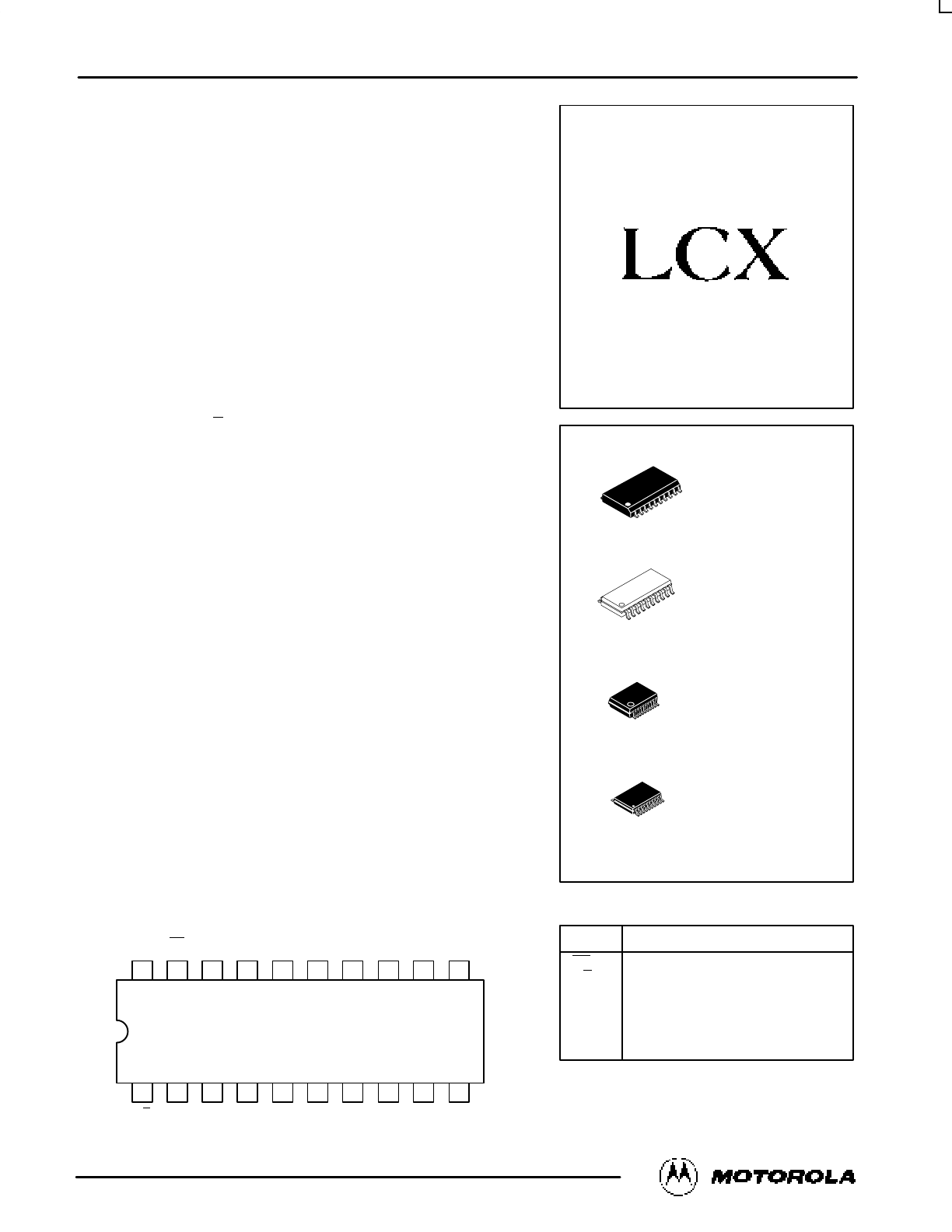
Pinout: 20–Lead (Top View)
19
20
18
17
16
15
14
2
1
3
4
5
6
7
VCC
13
8
12
9
11
10
OE
B0
B1
B2
B3
B4
B5
B6
B7
T/R
A0
A1
A2
A3
A4
A5
A6
A7
GND
DW SUFFIX
PLASTIC SOIC
CASE 751D–04
DT SUFFIX
PLASTIC TSSOP
CASE 948E–02
20
1
20
1
M SUFFIX
PLASTIC SOIC EIAJ
CASE 967–01
20
1
SD SUFFIX
PLASTIC SSOP
CASE 940C–03
20
1
LOW–VOLTAGE CMOS
OCTAL TRANSCEIVER
PIN NAMES
Function
Output Enable Input
Transmit/Receive Input
Side A 3–State Inputs or 3–State
Outputs
Side B 3–State Inputs or 3–State
Outputs
Pins
OE
T/R
A0–A7
B0–B7
MC74LCX245
MOTOROLA
LCX DATA
BR1339 — REV 2
2
B0
OE 19
T/R 1
A0
B1
A1
B2
A2
B3
A3
B4
A4
B5
A5
B6
A6
B7
A7
LOGIC DIAGRAM
2
3
4
5
6
7
8
9
18
17
16
15
14
13
12
11
INPUTS
OPERATING MODE
Non–Inverting
OE
T/R
OPERATING MODE
Non–Inverting
L
L
B Data to A Bus
L
H
A Data to B Bus
H
X
Z
H = High Voltage Level; L = Low Voltage Level; Z = High Impedance State; X = High or Low Voltage Level
and Transitions are Acceptable; For ICC reasons, Do Not Float Inputs
MC74LCX245
LCX DATA
BR1339 — REV 2
3
MOTOROLA
ABSOLUTE MAXIMUM RATINGS*
Symbol
Parameter
Value
Condition
Unit
VCC
DC Supply Voltage
–0.5 to +7.0
V
VI
DC Input Voltage
–0.5
≤
VI
≤
+7.0
V
VO
DC Output Voltage
–0.5
≤
VO
≤
+7.0
Output in 3–State
V
–0.5
≤
VO
≤
VCC + 0.51
Output in HIGH or LOW State
V
IIK
DC Input Diode Current
–50
VI < GND
mA
IOK
DC Output Diode Current
–50
VO < GND
mA
+50
VO > VCC
mA
IO
DC Output Source/Sink Current
±
50
mA
ICC
DC Supply Current Per Supply Pin
±
100
mA
IGND
DC Ground Current Per Ground Pin
±
100
mA
TSTG
Storage Temperature Range
–65 to +150
°
C
* Absolute maximum continuous ratings are those values beyond which damage to the device may occur. Exposure to these conditions or conditions
beyond those indicated may adversely affect device reliability. Functional operation under absolute–maximum–rated conditions is not implied.
1. IO absolute maximum rating must be observed.
RECOMMENDED OPERATING CONDITIONS
Symbol
Parameter
Min
Typ
Max
Unit
VCC
Supply Voltage
Operating
Data Retention Only
2.0
1.5
3.3
3.3
3.6
3.6
V
VI
Input Voltage
0
5.5
V
VO
Output Voltage
(HIGH or LOW State)
(3–State)
0
0
VCC
5.5
V
IOH
HIGH Level Output Current, VCC = 3.0V – 3.6V
–24
mA
IOL
LOW Level Output Current, VCC = 3.0V – 3.6V
24
mA
IOH
HIGH Level Output Current, VCC = 2.7V – 3.0V
–12
mA
IOL
LOW Level Output Current, VCC = 2.7V – 3.0V
12
mA
TA
Operating Free–Air Temperature
–40
+85
°
C
∆
t/
∆
V
Input Transition Rise or Fall Rate, VIN from 0.8V to 2.0V,
VCC = 3.0V
0
10
ns/V
DC ELECTRICAL CHARACTERISTICS
TA = –40
°
C to +85
°
C
Symbol
Characteristic
Condition
Min
Max
Unit
VIH
HIGH Level Input Voltage (Note 1)
2.7V
≤
VCC
≤
3.6V
2.0
V
VIL
LOW Level Input Voltage (Note 1)
2.7V
≤
VCC
≤
3.6V
0.8
V
VOH
HIGH Level Output Voltage
2.7V
≤
VCC
≤
3.6V; IOH = –100
µ
A
VCC – 0.2
V
VCC = 2.7V; IOH = –12mA
2.2
VCC = 3.0V; IOH = –18mA
2.4
VCC = 3.0V; IOH = –24mA
2.2
VOL
LOW Level Output Voltage
2.7V
≤
VCC
≤
3.6V; IOL = 100
µ
A
0.2
V
VCC = 2.7V; IOL= 12mA
0.4
VCC = 3.0V; IOL = 16mA
0.4
VCC = 3.0V; IOL = 24mA
0.55
1. These values of VI are used to test DC electrical characteristics only. Functional test should use VIH
≥
2.4V, VIL
≤
0.5V.
MC74LCX245
MOTOROLA
LCX DATA
BR1339 — REV 2
4
DC ELECTRICAL CHARACTERISTICS
(continued)
TA = –40
°
C to +85
°
C
Symbol
Characteristic
Condition
Min
Max
Unit
II
Input Leakage Current
2.7V
≤
VCC
≤
3.6V; 0V
≤
VI
≤
5.5V
±
5.0
µ
A
IOZ
3–State Output Current
2.7
≤
VCC
≤
3.6V; 0V
≤
VO
≤
5.5V;
VI = VIH or V IL
±
5.0
µ
A
IOFF
Power–Off Leakage Current
VCC = 0V; VI or VO = 5.5V
10
µ
A
ICC
Quiescent Supply Current
2.7
≤
VCC
≤
3.6V; VI = GND or VCC
10
µ
A
CC
2.7
≤
VCC
≤
3.6V; 3.6
≤
VI or VO
≤
5.5V
±
10
µ
A
∆
ICC
Increase in ICC per Input
2.7
≤
VCC
≤
3.6V; VIH = VCC – 0.6V
500
µ
A
AC CHARACTERISTICS (tR = tF = 2.5ns; CL = 50pF; RL = 500
Ω
)
Limits
TA = –40
°
C to +85
°
C
VCC = 3.0V to 3.6V
VCC = 2.7V
Symbol
Parameter
Waveform
Min
Max
Max
Unit
tPLH
tPHL
Propagation Delay
Input to Output
1
1.5
1.5
7.0
7.0
8.0
8.0
ns
tPZH
tPZL
Output Enable Time to
High and Low Level
2
1.5
1.5
8.5
8.5
9.5
9.5
ns
tPHZ
tPLZ
Output Disable Time From
High and Low Level
2
1.5
1.5
7.5
7.5
8.5
8.5
ns
tOSHL
tOSLH
Output–to–Output Skew
(Note 1)
1.0
1.0
ns
1. Skew is defined as the absolute value of the difference between the actual propagation delay for any two separate outputs of the same device.
The specification applies to any outputs switching in the same direction, either HIGH–to–LOW (tOSHL) or LOW–to–HIGH (tOSLH); parameter
guaranteed by design.
DYNAMIC SWITCHING CHARACTERISTICS
TA = +25
°
C
Symbol
Characteristic
Condition
Min
Typ
Max
Unit
VOLP
Dynamic LOW Peak Voltage1
VCC = 3.3V, CL = 50pF, VIH = 3.3V, VIL = 0V
0.8
V
VOLV
Dynamic LOW Valley Voltage1
VCC = 3.3V, CL = 50pF, VIH = 3.3V, VIL = 0V
0.8
V
1. Number of outputs defined as “n”. Measured with “n–1” outputs switching from HIGH–to–LOW or LOW–to–HIGH. The remaining output is
measured in the LOW state.
CAPACITIVE CHARACTERISTICS
Symbol
Parameter
Condition
Typical
Unit
CPD
Power Dissipation Capacitance
10MHz, VCC = 3.3V, VI = 0V or VCC
25
pF
CIN
Input Capacitance
VCC = 3.3V, VI = 0V or VCC
7
pF
CI/O
Input/Output Capacitance
VCC = 3.3V, VI = 0V or VCC
8
pF
MC74LCX245
LCX DATA
BR1339 — REV 2
5
MOTOROLA
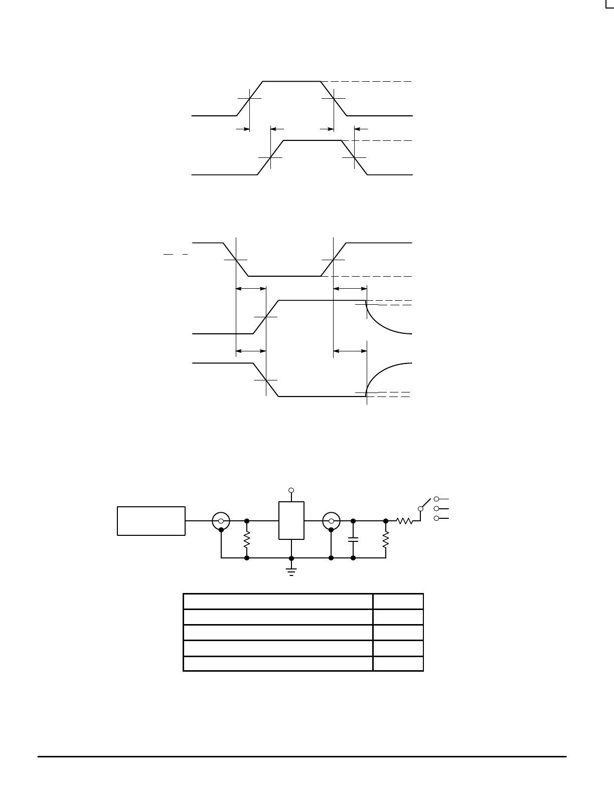
WAVEFORM 1 – PROPAGATION DELAYS
tR = tF = 2.5ns, 10% to 90%; f = 1MHz; tW = 500ns
2.7V
0V
VOH
VOL
An, Bn
Bn, An
tPHL
tPLH
WAVEFORM 2 – OUTPUT ENABLE AND DISABLE TIMES
tR = tF = 2.5ns, 10% to 90%; f = 1MHz; tW = 500ns
2.7V
0V
≈
0V
OE, T/R
An, Bn
tPZH
≈
3.0V
tPHZ
tPZL
tPLZ
An, Bn
1.5V
1.5V
1.5V
1.5V
1.5V
1.5V
Figure 1. AC Waveforms
1.5V
VCC
VOH – 0.3V
VOL + 0.3V
GND
1.5V
OPEN
PULSE
GENERATOR
RT
DUT
VCC
RL
R1
CL
6V
GND
TEST
SWITCH
tPLH, tPHL
Open
tPZL, tPLZ
6V
Open Collector/Drain tPLH and tPHL
6V
tPZH, tPHZ
GND
CL = 50pF or equivalent (Includes jig and probe capacitance)
RL = R1 = 500
Ω
or equivalent
RT = ZOUT of pulse generator (typically 50
Ω
)
Figure 2. Test Circuit
MC74LCX245
MOTOROLA
LCX DATA
BR1339 — REV 2
6
OUTLINE DIMENSIONS
DW SUFFIX
PLASTIC SOIC PACKAGE
CASE 751D–04
ISSUE E
M SUFFIX
PLASTIC SOIC EIAJ PACKAGE
CASE 967–01
ISSUE O
MIN
MIN
MAX
MAX
MILLIMETERS
INCHES
DIM
A
B
C
D
F
G
J
K
M
P
R
0.510
0.299
0.104
0.019
0.035
0.012
0.009
7
°
0.415
0.029
0.499
0.292
0.093
0.014
0.020
0.010
0.004
0
°
0.395
0.010
12.95
7.60
2.65
0.49
0.90
0.32
0.25
7
°
10.55
0.75
12.65
7.40
2.35
0.35
0.50
0.25
0.10
0
°
10.05
0.25
NOTES:
1. DIMENSIONING AND TOLERANCING PER
ANSI Y14.5M, 1982.
2. CONTROLLING DIMENSION: MILLIMETER.
3. DIMENSIONS A AND B DO NOT INCLUDE
MOLD PROTRUSION.
4. MAXIMUM MOLD PROTRUSION 0.150
(0.006) PER SIDE.
5. DIMENSION D DOES NOT INCLUDE
DAMBAR PROTRUSION. ALLOWABLE
DAMBAR PROTRUSION SHALL BE 0.13
(0.005) TOTAL IN EXCESS OF D DIMENSION
AT MAXIMUM MATERIAL CONDITION.
1.27 BSC
0.050 BSC
–A
–
–B
–
P
10 PL
1
10
11
20
–T
–
D
20 PL
K
C
SEATING
PLANE
R
X 45
°
M
0.010 (0.25)
B
M
M
0.010 (0.25)
T
A
B
M
S
S
G
18 PL
F
J
DIM
MIN
MAX
MIN
MAX
INCHES
---
2.05
---
0.081
MILLIMETERS
0.05
0.20
0.002
0.008
0.35
0.50
0.014
0.020
0.18
0.27
0.007
0.011
12.35
12.80
0.486
0.504
5.10
5.45
0.201
0.215
1.27 BSC
0.050 BSC
7.40
8.20
0.291
0.323
0.50
0.85
0.020
0.033
1.10
1.50
0.043
0.059
0
0.70
0.90
0.028
0.035
---
0.81
---
0.032
A1
A
b
c
D
E
e
L
M
Z
HE
Q1
LE
_
10
_
0
_
10
_
NOTES:
1 DIMENSIONING AND TOLERANCING PER ANSI
Y14.5M, 1982.
2 CONTROLLING DIMENSION: MILLIMETER.
3 DIMENSIONS D AND E DO NOT INCLUDE MOLD
FLASH OR PROTRUSIONS AND ARE MEASURED
AT THE PARTING LINE. MOLD FLASH OR
PROTRUSIONS SHALL NOT EXCEED 0.15 (0.006)
PER SIDE.
4 TERMINAL NUMBERS ARE SHOWN FOR
REFERENCE ONLY.
5 THE LEAD WIDTH DIMENSION (b) DOES NOT
INCLUDE DAMBAR PROTRUSION. ALLOWABLE
DAMBAR PROTRUSION SHALL BE 0.08 (0.003)
TOTAL IN EXCESS OF THE LEAD WIDTH
DIMENSION AT MAXIMUM MATERIAL CONDITION.
DAMBAR CANNOT BE LOCATED ON THE LOWER
RADIUS OR THE FOOT. MINIMUM SPACE
BETWEEN PROTRUSIONS AND ADJACENT LEAD
TO BE 0.46 ( 0.018).
Z
D
HE
E
1
20
11
10
b
A1
e
L
LE
Q1
M
_
VIEW P
DETAIL P
0.13 (0.005)
M
0.10 (0.004)
c
A
MC74LCX245
LCX DATA
BR1339 — REV 2
7
MOTOROLA
OUTLINE DIMENSIONS
SD SUFFIX
PLASTIC SSOP PACKAGE
CASE 940C–03
ISSUE B
DT SUFFIX
PLASTIC TSSOP PACKAGE
CASE 948E–02
ISSUE A
DIM
A
MIN
MAX
MIN
MAX
INCHES
6.60
0.260
MILLIMETERS
B
4.30
4.50
0.169
0.177
C
1.20
0.047
D
0.05
0.15
0.002
0.006
F
0.50
0.75
0.020
0.030
G
0.65 BSC
0.026 BSC
H
0.27
0.37
0.011
0.015
J
0.09
0.20
0.004
0.008
J1
0.09
0.16
0.004
0.006
K
0.19
0.30
0.007
0.012
K1
0.19
0.25
0.007
0.010
L
6.40 BSC
0.252 BSC
M
0
8
0
8
_
_
_
_
NOTES:
6 DIMENSIONING AND TOLERANCING PER ANSI
Y14.5M, 1982.
7 CONTROLLING DIMENSION: MILLIMETER.
8 DIMENSION A DOES NOT INCLUDE MOLD FLASH,
PROTRUSIONS OR GATE BURRS. MOLD FLASH
OR GATE BURRS SHALL NOT EXCEED 0.15
(0.006) PER SIDE.
9 DIMENSION B DOES NOT INCLUDE INTERLEAD
FLASH OR PROTRUSION. INTERLEAD FLASH OR
PROTRUSION SHALL NOT EXCEED 0.25 (0.010)
PER SIDE.
10 DIMENSION K DOES NOT INCLUDE DAMBAR
PROTRUSION. ALLOWABLE DAMBAR
PROTRUSION SHALL BE 0.08 (0.003) TOTAL IN
EXCESS OF THE K DIMENSION AT MAXIMUM
MATERIAL CONDITION.
11 TERMINAL NUMBERS ARE SHOWN FOR
REFERENCE ONLY.
12 DIMENSION A AND B ARE TO BE DETERMINED
AT DATUM PLANE –W–.
ÍÍÍÍ
ÍÍÍÍ
ÍÍÍÍ
ÍÍÍÍ
ÍÍÍÍ
1
10
11
20
PIN 1
IDENT
A
B
–T–
0.100 (0.004)
C
D
G
H
SECTION N–N
K
K1
J J1
N
N
M
F
–W–
SEATING
PLANE
–V–
–U–
S
U
M
0.10 (0.004)
V
S
T
20X REF
K
L
L/2
2X
S
U
0.15 (0.006) T
DETAIL E
0.25 (0.010)
DETAIL E
6.40
0.252
–––
–––
S
U
0.15 (0.006) T
20
11
10
1
H
A
B
F
M
K
20X REF
S
U
M
0.12 (0.005)
V
S
T
L
L/2
PIN 1
IDENT
S
U
M
0.20 (0.008)
T
–V–
–U–
D
C
0.076 (0.003)
G
–T–
SEATING
PLANE
DETAIL E
N
N
0.25 (0.010)
ÇÇÇ
ÇÇÇ
ÇÇÇ
ÇÇÇ
ÉÉÉ
ÉÉÉ
ÉÉÉ
ÉÉÉ
K
J
J1
K1
SECTION N–N
DIM
A
MIN
MAX
MIN
MAX
INCHES
7.07
7.33
0.278
0.288
MILLIMETERS
B
5.20
5.38
0.205
0.212
C
1.73
1.99
0.068
0.078
D
0.05
0.21
0.002
0.008
F
0.63
0.95
0.024
0.037
G
0.65 BSC
0.026 BSC
H
0.59
0.75
0.023
0.030
J
0.09
0.20
0.003
0.008
J1
0.09
0.16
0.003
0.006
K
0.25
0.38
0.010
0.015
K1
0.25
0.33
0.010
0.013
_
_
_
_
NOTES:
13 DIMENSIONING AND TOLERANCING PER ANSI
Y14.5M, 1982.
14 CONTROLLING DIMENSION: MILLIMETER.
15 DIMENSION A DOES NOT INCLUDE MOLD FLASH,
PROTRUSIONS OR GATE BURRS. MOLD FLASH
OR GATE BURRS SHALL NOT EXCEED 0.15
(0.006) PER SIDE.
16 DIMENSION B DOES NOT INCLUDE INTERLEAD
FLASH OR PROTRUSION. INTERLEAD FLASH OR
PROTRUSION SHALL NOT EXCEED 0.15 (0.006)
PER SIDE.
17 DIMENSION K DOES NOT INCLUDE DAMBAR
PROTRUSION/INTRUSION. ALLOWABLE DAMBAR
PROTRUSION SHALL BE 0.13 (0.005) TOTAL IN
EXCESS OF K DIMENSION AT MAXIMUM
MATERIAL CONDITION. DAMBAR INTRUSION
SHALL NOT REDUCE DIMENSION K BY MORE
THAN 0.07 (0.002) AT LEAST MATERIAL
CONDITION.
18 TERMINAL NUMBERS ARE SHOWN FOR
REFERENCE ONLY.
19 DIMENSION A AND B ARE TO BE DETERMINED
AT DATUM PLANE –W–.
L
7.65
7.90
0.301
0.311
M
0
8
0
8
DETAIL E
–W–
MC74LCX245
MOTOROLA
LCX DATA
BR1339 — REV 2
8
How to reach us:
USA/EUROPE: Motorola Literature Distribution;
JAPAN: Nippon Motorola Ltd.; Tatsumi–SPD–JLDC, Toshikatsu Otsuki,
P.O. Box 20912; Phoenix, Arizona 85036. 1–800–441–2447
6F Seibu–Butsuryu–Center, 3–14–2 Tatsumi Koto–Ku, Tokyo 135, Japan. 03–3521–8315
MFAX: RMFAX0@email.sps.mot.com –TOUCHTONE (602) 244–6609
HONG KONG: Motorola Semiconductors H.K. Ltd.; 8B Tai Ping Industrial Park,
INTERNET: http://Design–NET.com
51 Ting Kok Road, Tai Po, N.T., Hong Kong. 852–26629298
Motorola reserves the right to make changes without further notice to any products herein. Motorola makes no warranty, representation or guarantee regarding
the suitability of its products for any particular purpose, nor does Motorola assume any liability arising out of the application or use of any product or circuit,
and specifically disclaims any and all liability, including without limitation consequential or incidental damages. “Typical” parameters can and do vary in different
applications. All operating parameters, including “Typicals” must be validated for each customer application by customer’s technical experts. Motorola does
not convey any license under its patent rights nor the rights of others. Motorola products are not designed, intended, or authorized for use as components in
systems intended for surgical implant into the body, or other applications intended to support or sustain life, or for any other application in which the failure of
the Motorola product could create a situation where personal injury or death may occur. Should Buyer purchase or use Motorola products for any such
unintended or unauthorized application, Buyer shall indemnify and hold Motorola and its officers, employees, subsidiaries, affiliates, and distributors harmless
against all claims, costs, damages, and expenses, and reasonable attorney fees arising out of, directly or indirectly, any claim of personal injury or death
associated with such unintended or unauthorized use, even if such claim alleges that Motorola was negligent regarding the design or manufacture of the part.
Motorola and
are registered trademarks of Motorola, Inc. Motorola, Inc. is an Equal Opportunity/Affirmative Action Employer.
MC74LCX245/D
*MC74LCX245/D*
◊
CODELINE