
R&E International
A Subsidiary of Microchip Technology Inc.
RE46C119
Voltage Regulator, Voltage Converter and Piezoelectric Horn Driver
Product Specification
© 2009 Microchip Technology Inc. DS22169A-page 1
General Description
The RE46C119 is intended for use in applications
where low voltage regulation and a high voltage
horn driver are required. The circuit features a
voltage boost converter/regulator and driver circuit
suitable for driving a piezoelectric horn. The horn
enable pin activates the boost converter and horn
driver circuit. Supply current is 6.5uA maximum
when the boost regulator and horn driver are not in
use. A 3V regulator is also provided for
microprocessor voltage regulation. Low battery
detection and signaling are also available.
Interconnect pins are provided to allow
communication in multiple unit environments. A
power good pin monitors the status of the regulator
output.
Applications
Smoke detectors
CO Detectors
Personal Security Products
Electronic Games
Hand Held Instruments
Features
• Low Quiescent Current
• 12V Boost Regulator
• Low Horn Driver Ron
• 3V Regulator, Other Options Available
• Low Battery Detection Interface
• Power Good Circuit
• Device
interconnection
• Available in DIP and SOIC packages
•
Available in Standard Packaging or RoHS
Compliant Pb Free Packaging
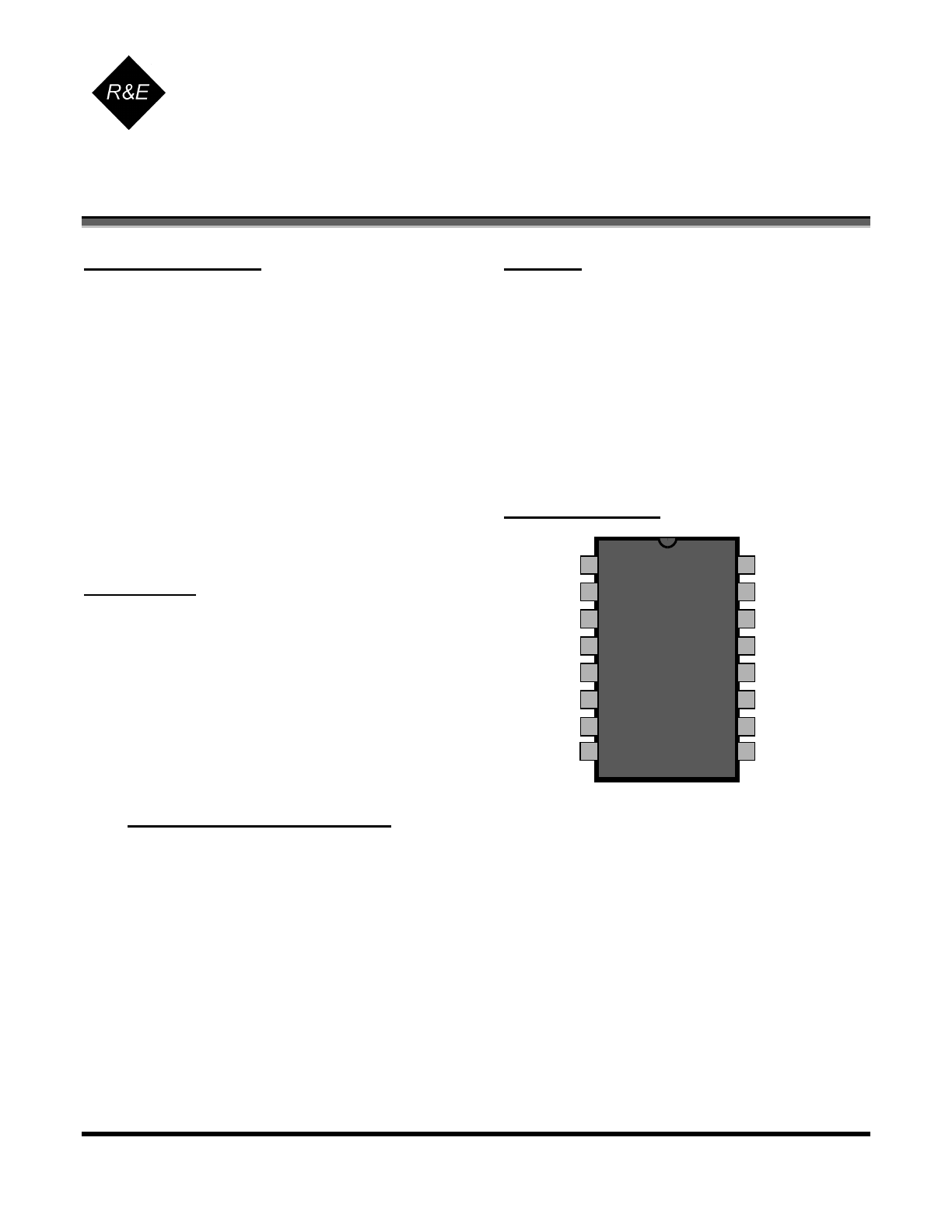
Pin Configuration
1
16
VDD
IO1
IODIR
IO2
LBST
PG
HRNEN
VSS
VPOS
CAP+
CAP-
VREG
LBAT
HORNB
HORNS
FEED
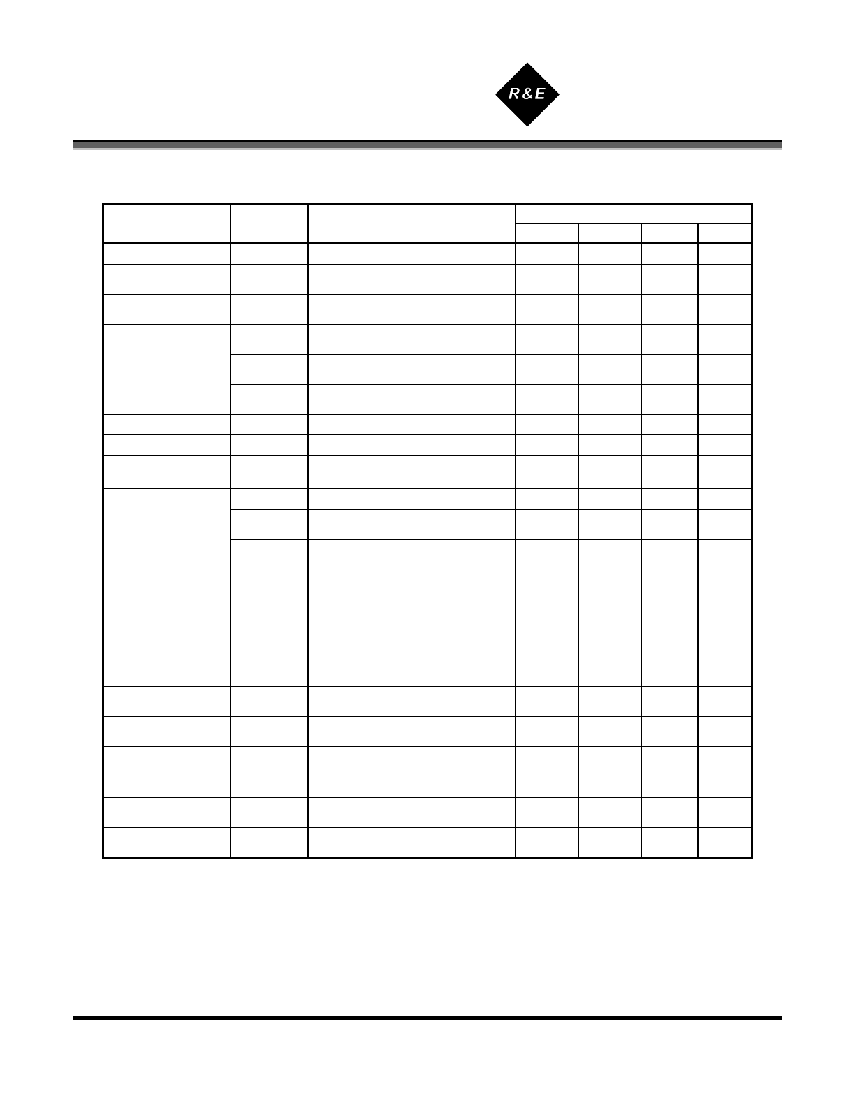
ABSOLUTE MAXIMUM RATINGS
PARAMETER
SYMBOL VALUE UNITS
Supply Voltage
V
DD
12 V
Input Voltage Range Except FEED, IO1, IO2
V
in
-.3 to V
dd
+.3 V
FEED Input Voltage Range
V
infd
-10 to +22
V
IO2 Input Voltage Range
V
io2
-.3 to VREG+.3
V
IO1 (as input) Voltage Range
V
io1
-.3 to V
dd
+ 6
V
Input Current except FEED
I
in
10 mA
Operating Temperature
T
A
-40 to 85
°C
Continuous Operating Current (Horn or VPOS)
I
con
50 mA
Storage Temperature
T
STG
-55 to 125
°C
Maximum Junction Temperature
T
J
125
°C
Stresses beyond those listed under Absolute Maximum Ratings may cause permanent damage to the device. These are
stress ratings only and operation at these conditions for extended periods may affect device reliability.
This product utilizes CMOS technology with static protection; however proper ESD prevention procedures should be used
when handling this product. Damage can occur when exposed to extremely high static electrical charges.
RE46C119
Voltage Regulator, Voltage Converter and R&E International
Piezoelectric Horn Driver
A Subsidiary of Microchip Technology
Inc.
Product Specification
© 2009 Microchip Technology Inc. DS22169A-page 2
Electrical Characteristics at T
A
=27°C, Vdd=9V, Vss=0V (unless otherwise noted).
Limits
Parameter
Symbol Conditions
MIN TYP MAX
UNITS
Supply Voltage
Vdd
Operating
6 12
V
Quiescent Supply
Current
Idd1
HRNEN, LBST, IODIR, FEED,
REGSEL=VSS, No Loads
4.7
6.5
uA
Supply Current
Idd2
LBST, IODIR, FEED =VSS
HRNEN=VDD, No Loads
350 uA
Iin
All Inputs except FEED, Vin=VDD
or VSS
-100 100
nA
Iihf
FEED=+22V
20
50
uA
Input Leakage
Iilf
FEED=-10V
-50 -15 uA
Output Leakage
Iout
PG = 5.0v
1.0
uA
Input Voltage Low
Vil
All Inputs except FEED
1
V
Input Voltage
High
Vih
All Inputs Except FEED
2.3
V
Vol1
HORNB or HORNS; Iout=16mA;
.3
.5
V
Vol2
IO2, Iout=100uA;
IODIR=Vil , IO1=Vil
.3
.5
V
Output Low Voltage
Vol3
PG, Iout=5.0mA;
.5
V
Voh1
HORNB or HORNS; Iout=-16mA Vpos-.5 Vpos-.3
V
Output High
Voltage
Voh2
IO2, Iout=-100uA;
IODIR=Vil , IO1=Vih
Vreg -.5
Vreg -.3
V
VPOS RMS Output
Voltage
V
vpos
VPOS; Iout=-16mA;
HRNEN=VDD
10.7 11.8
12.7
V
Charge pump
Oscillator
Frequency
CPf
150 kHz
Charge pump
Power Efficiency
CPpe
VPOS; Iout=-16mA, C1=1uF
C2=10uF; Vdd=6.5v
85 %
Charge pump
Voltage Efficiency
CPve
VPOS; No Loads, C1=1uF
C2=10uF; Vdd=6.0v
95 99 %
Low Battery
Interface
Lbv LBAT;
LBST=Vdd
.17 *Vdd
.2*Vdd
.23*Vdd
V
VREG Voltage
Vreg
VREG; Iout<50mA; HRNEN=VSS
2.85
3
3.15
V
VREG Line
Regulation
Vregln
VREG; Vdd=6V to 12V; VREG
Iout=10mA; HRNEN = VSS
; Note 3
50
mV
VREG Load
Regulation
Vregld
VREG; Iout=0 to -50mA;
HRNEN=VSS;
Note 3
90
mV
RE46C119
Voltage Regulator, Voltage Converter and R&E International
Piezoelectric Horn Driver
A Subsidiary of Microchip Technology
Inc.
Product Specification
© 2009 Microchip Technology Inc. DS22169A-page 3
Electrical Characteristics at T
A
=27°C, Vdd=9V, Vss=0V (unless otherwise noted).
Limits
Parameter
Symbol Conditions
MIN TYP
MAX
UNITS
VREG Over
Voltage Clamp
Vcl
Iout>1mA; Note 2
3.7
4.0
4.3
V
VREG Over
Voltage
Clamp Current
Icl VREG≥Vcl 0.5
mA
PGvtr
Vreg output rising
77
84
94
%Vreg
PG Trip Threshold
PGvtf
Vreg output falling
72
80
88
%Vreg
PG Delay
PGtdly
Delay time with respect to PGvtr
500
usec
IO1ih1
IODIR=Vil, IO1=Vdd-2V, Vdd=12V
25
60
UA
IO1ih2
IODIR=Vil, IO1=17V, Vdd=12V
150
UA
IO1ioh1
IODIR, IO2=Vih, Vdd=6.5V,
IO1=4.5V
-4
mA
IO1ioh2
IODIR, IO2=Vih, Vdd=12V,
IO1=Vss
-16
mA
IO1 Output Current
IO1iol1
IO dump current
IODIR= Vih, IO2=Vil, IO1=1V
10 15 mA
IO1vih IODIR=Vil
3
V
IO1 Alarm Voltage
IO1vil IODIR=Vil
1.5 V
Unless noted the limits at room temperature are guaranteed and 100% production tested. Limits over temperature are guaranteed but not
100% tested.
Note 2: In normal operation, the regulator will provide high-side current of up to 50mA, but current sinking capability is typically under 1uA. The
overvoltage clamp, Vcl is intended to limit the voltage at VREG (output) when it is pulled up by an external source.
Note 3: Not 100% production tested but limits are guaranteed by design.
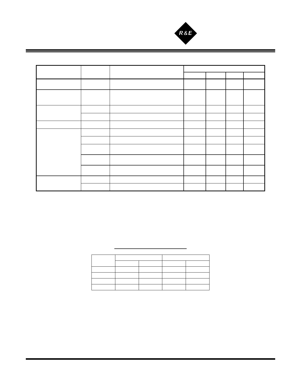
Interconnect Logic Truth Table
IO2 (pin 4)
IO1 (pin 2)
IODIR
(pin 3)
Input Output Input Output
1 0 0
1 1 1
0 0 0
0 1 1
RE46C119
Voltage Regulator, Voltage Converter and R&E International
Piezoelectric Horn Driver
A Subsidiary of Microchip Technology
Inc.
Product Specification
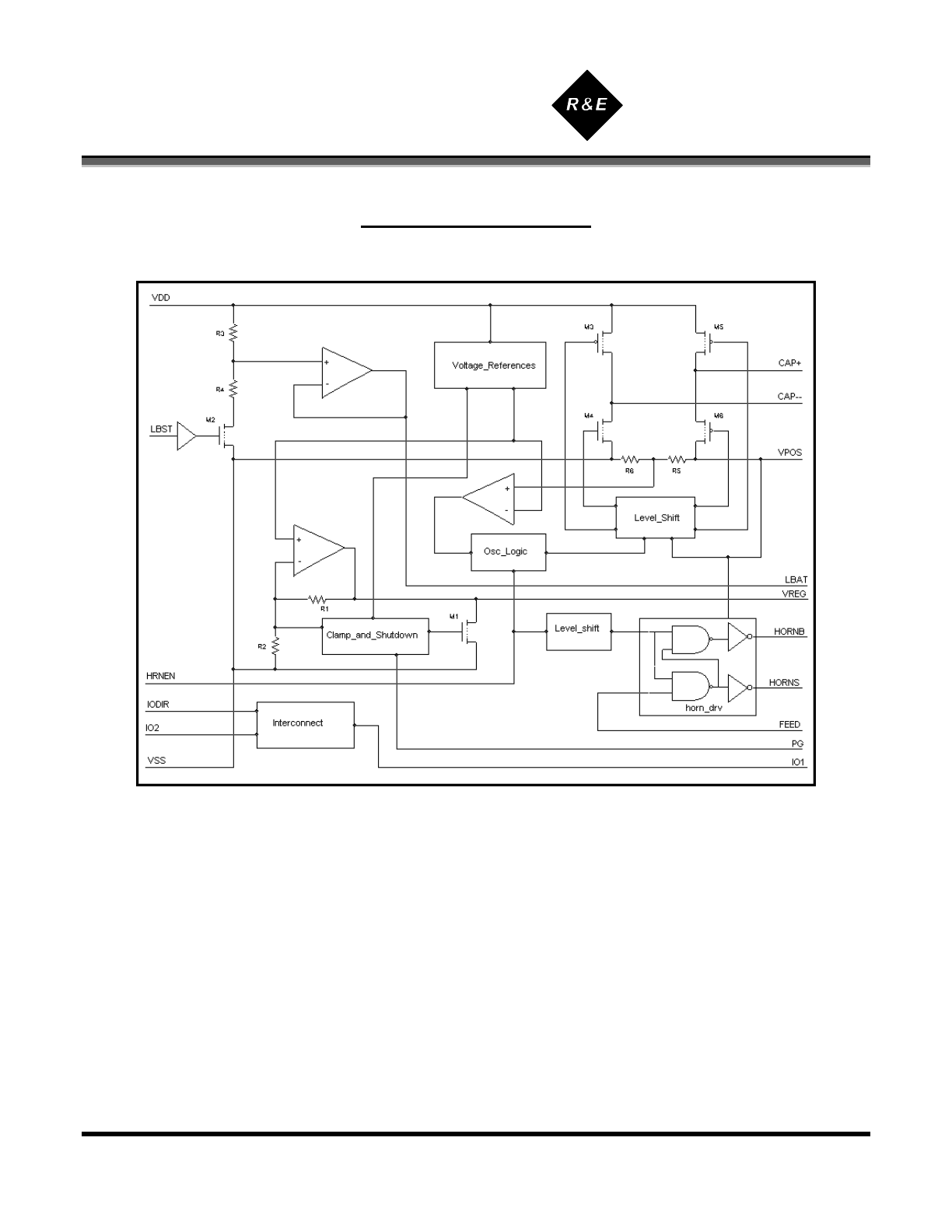
Functional Block Diagram
© 2009 Microchip Technology Inc. DS22169A-page 4

RE46C119
Voltage Regulator, Voltage Converter and R&E International
Piezoelectric Horn Driver
A Subsidiary of Microchip Technology
Inc.
Product Specification
© 2009 Microchip Technology Inc. DS22169A-page 5
PIN DESCRIPTIONS
VDD
(Pin 1, Input) - Connect to the positive
terminal of the supply voltage for the voltage
regulator, charge pump voltage converter
and bi-directional Interconnect block.
IO1
(Pin 2, Input/Output) - This bi-directional
pin provides an interface to additional
RE46C119 IO1 pins. This serves as a
communication link between separate
modules.
IODIR
(Pin 3, Input) - This input provides
control for the bi-directional pins IO1 and
IO2.
IO2
(Pin 4, Input/Output) - This bi-directional
pin provides an interface to a TTL/CMOS I/O
of an uP or ASIC. Refer to the interconnect
logic truth table.
LBST
(Pin 5, Input) - This input provides an
enable or strobe control for the analog low
battery detection function.
PG
(Pin 6, Output) - This open drain NMOS
output provides a status indication of when
the VREG output is above or below a
specified voltage level.
HRNEN
(Pin 7, Input) - This input provides
activation control for the charge pump boost
regulator and horn driver outputs.
VSS
(Pin 8, Input) - This power pin is
connected to the negative terminal of the
supply voltage.
FEEDBACK
(Pin9, Input) - Horn driver
input.
HORNS
(Pin10, Output) - Horn output driver
which provides VPOS to VSS output voltage
swing for the piezoelectric horn.
HORNB
(Pin11, Output) - Horn output driver
which provides VPOS to VSS output voltage
swing for the piezoelectric horn.
LBAT
(Pin12, Output) - Analog output
voltage that is proportional to the VDD
supply and functions as a low battery
detection output.
VREG
(Pin13, Output) - Voltage regulator
output, requires an external capacitor.
VCAP-
(Pin14, I/O) - Negative terminal for
the external charge pump boost (fly)
capacitor.
VCAP+
(Pin 15, I/O) - Positive terminal for
the external charge pump boost (fly)
capacitor.
VPOS
(Pin 16, Output) - This output pin
requires an external filter capacitor which
supplies voltage for the horn driver outputs.

RE46C119
Voltage Regulator, Voltage Converter and R&E International
Piezoelectric Horn Driver
A Subsidiary of Microchip Technology
Inc.
Product Specification
© 2009 Microchip Technology Inc. DS22169A-page 6
Device Operation
(Please refer to the functional block diagram)
The RE46C119 consists of the following main functional blocks: band gap voltage reference, low drop-out voltage
regulator (with over voltage clamp and power supply brownout protection), low battery detection, switched
capacitor 12 volt boost regulator, horn driver and Interconnect logic.
When power is applied the band gap voltage reference and the voltage regulator output are initially enabled. The
low battery detection, horn driver outputs and switched capacitor 12v boost regulator are enabled by TTL
compatible positive logic control inputs.
When the HRNEN (Horn Enable) input is brought to a logic high level, the horn driver outputs as well as the 12v
boost regulator become active. The 12v boost regulator supplies the horn driver outputs. The 12v boost regulator
utilizes a charge pump to boost the Vdd supply input to a regulated 12-volt output. The charge pump consists of
an internal oscillator that is controlled in a voltage comparator feedback configuration.
The low battery detection is enabled and strobed when the LBST input is brought to a logic high level. The LBAT
output is a voltage follower amplifier whose input is determined by a resistor divider across the device supply rails.
RE46C119
Voltage Regulator, Voltage Converter and R&E International
Piezoelectric Horn Driver
A Subsidiary of Microchip Technology
Inc.
Product Specification
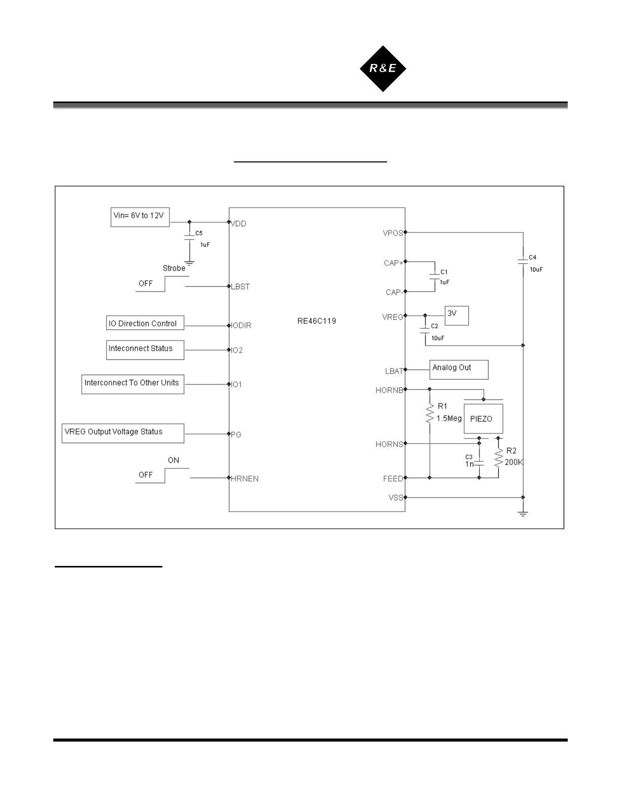
Typical Application Circuit
Application Notes:
(See application circuit)
The efficiency of the switched capacitor charge pump regulator varies with the applied input voltage and the load
current. The approximate voltage efficiency is given by:
Efficiency (%) = [VPOS/(2xVDD)]x100
© 2009 Microchip Technology Inc. DS22169A-page 7

RE46C119
Voltage Regulator, Voltage Converter and R&E International
Piezoelectric Horn Driver
A Subsidiary of Microchip Technology
Inc.
Product Specification
© 2009 Microchip Technology Inc. DS22169A-page 8
Application Notes continued:
(See application circuit)
Capacitor Selection:
To achieve minimum output voltage ripple, the output capacitor C
4
(for VPOS) should have a low ESR (Effective
Series Resistance) value with leads kept as short as possible. Capacitors with long leads increase ripple voltage
due to lead inductance.
Like all Low-Dropout Regulators, the RE46C119 requires an output capacitor connected between VREG (output)
and VSS to stabilize the internal control loop. The recommended capacitance is 10uF. Capacitor values larger
than 10uF are acceptable.
PCB Layout Suggestions:
Due to large transient currents flow in the V
DD
, V
POS
and V
SS
terminals, minimizing both input and output ripple is
accomplished by placing capacitors as close as possible to the regulator using short direct circuit wiring or traces.
RE46C119
Voltage Regulator, Voltage Converter and R&E International
Piezoelectric Horn Driver
A Subsidiary of Microchip Technology
Inc.
Product Specification
Information contained in this publication regarding device
applications and the like is provided only for your convenience and
may be superseded by updates. It is your responsibility to ensure
that your application meets with your specifications. MICROCHIP
MAKES NO REPRESENTATIONS OR WARRANTIES OF ANY
KIND WHETHER EXPRESS OR IMPLIED, WRITTEN OR ORAL,
STATUTORY OR OTHERWISE, RELATED TO THE
INFORMATION, INCLUDING BUT NOT LIMITED TO ITS
CONDITION, QUALITY, PERFORMANCE, MERCHANTABILITY
OR FITNESS FOR PURPOSE. Microchip disclaims all liability
arising from this information and its use. Use of Microchip devices in
life support and/or safety applications is entirely at the buyer’s risk,
and the buyer agrees to defend, indemnify and hold harmless
Microchip from any and all damages, claims, suits, or expenses
resulting from such use. No licenses are conveyed, implicitly or
otherwise, under any Microchip intellectual property rights.
Trademarks
The Microchip name and logo, the Microchip logo, Accuron,
dsPIC, K
EE
L
OQ
, K
EE
L
OQ
logo,
MPLAB, PIC, PICmicro,
PICSTART, rfPIC, SmartShunt and UNI/O are registered
trademarks of Microchip Technology Incorporated in the U.S.A.
and other countries.
FilterLab, Hampshire, Linear Active Thermistor, MXDEV, MXLAB,
SEEVAL, SmartSensor and The Embedded Control Solutions
Company are registered trademarks of Microchip Technology
Incorporated in the U.S.A.
Analog-for-the-Digital Age, Application Maestro, CodeGuard,
dsPICDEM, dsPICDEM.net, dsPICworks, dsSPEAK, ECAN,
ECONOMONITOR, FanSense, In-Circuit Serial Programming,
ICSP, ICEPIC, Mindi, MiWi, MPASM, MPLAB Certified logo,
MPLIB, MPLINK, mTouch, nanoWatt XLP, PICkit, PICDEM,
PICDEM.net, PICtail, PIC
32
logo, PowerCal, PowerInfo,
PowerMate, PowerTool, REAL ICE, rfLAB, Select Mode, Total
Endurance, TSHARC, WiperLock and ZENA are trademarks of
Microchip Technology Incorporated in the U.S.A. and other
countries.
SQTP is a service mark of Microchip Technology Incorporated in
the U.S.A.
All other trademarks mentioned herein are property of their
respective companies.
© 2009, Microchip Technology Incorporated, Printed in the
U.S.A., All Rights Reserved.
Printed on recycled paper.
Microchip received ISO/TS-16949:2002 certification for its worldwide
headquarters, design and wafer fabrication facilities in Chandler and
Tempe, Arizona; Gresham, Oregon and design centers in California and
India. The Company’s quality system processes and procedures are for its
PIC
®
MCUs and dsPIC
®
DSCs, K
EE
L
OQ
®
code hopping devices, Serial
EEPROMs, microperipherals, nonvolatile memory and analog products. In
addition, Microchip’s quality system for the design and manufacture of
development systems is ISO 9001:2000 certified.
© 2009 Microchip Technology Inc. DS22169A-page 9