

2016-2018 Microchip Technology Inc.
DS00002237D-page 1
USB5807
Highlights
• USB Hub with 7 USB 3.1 Gen 1 / USB 2.0 down-
stream ports
• USB-IF Battery Charger revision 1.2 support on
up & downstream ports (DCP, CDP, SDP)
• FlexConnect: Downstream port able to swap with
upstream port, allowing master capable devices
to control other devices on the hub
• USB Link Power Management (LPM) support
• Enhanced OEM configuration options available
through either OTP or SPI ROM
• Available in 100-pin (12mm x 12mm) VQFN
RoHS compliant package
• Commercial and industrial grade temperature
support
Target Applications
• Standalone USB Hubs
• Laptop Docks
• PC Motherboards
• PC Monitor Docks
• Multi-function USB 3.1 Gen 1 Peripherals
Key Benefits
• USB 3.1 Gen 1 compliant 5 Gbps, 480 Mbps,
12 Mbps, and 1.5Mbps operation
- 5V tolerant USB 2.0 pins
- 1.32V tolerant USB 3.1 Gen 1 pins
- Integrated termination and pull-up/down resistors
• Supports battery charging of most popular battery
powered devices on all ports
- USB-IF Battery Charging rev. 1.2 support
(DCP, CDP, SDP)
- Apple
®
portable product charger emulation
- Chinese YD/T 1591-2006 charger emulation
- Chinese YD/T 1591-2009 charger emulation
- European Union universal mobile charger support
- Support for Microchip UCS100x family of battery
charging controllers
- Supports additional portable devices
• Smart port controller operation
- Firmware handling of companion port power
controllers
• On-chip microcontroller
- manages I/Os, VBUS, and other signals
• 8 KB RAM, 64 KB ROM
• 8 KB One-Time-Programmable (OTP) ROM
- Includes on-chip charge pump
• Configuration programming via OTP ROM,
SPI ROM, or SMBus
• FlexConnect
- Reversible upstream and downstream Port 1 roles
on command
• PortSwap
- Configurable USB 2.0 differential pair signal swap
• PHYBoost
TM
- Programmable USB transceiver drive strength for
recovering signal integrity
• VariSense
TM
- Programmable USB receive sensitivity
• Port Split
- USB2.0 and USB3.1 Gen1 port operation can be
split for custom applications using embedded
USB3.x devices in parallel with USB2.0 devices.
• Compatible with Microsoft Windows 10, 8, 7, XP,
Apple OS X 10.4+, and Linux hub drivers
• Optimized for low-power operation and low ther-
mal dissipation
• Package
- 100-pin VQFN (12mm x 12mm)
7-Port USB 3.1 Gen 1 Hub

USB5807
DS00002237D-page 2
2016-2018 Microchip Technology Inc.
TO OUR VALUED CUSTOMERS
It is our intention to provide our valued customers with the best documentation possible to ensure successful use of your Microchip
products. To this end, we will continue to improve our publications to better suit your needs. Our publications will be refined and
enhanced as new volumes and updates are introduced.
If you have any questions or comments regarding this publication, please contact the Marketing Communications Department via
E-mail at
docerrors@microchip.com
or fax the Reader Response Form in the back of this data sheet to (480) 792-4150. We
welcome your feedback.
Most Current Data Sheet
To obtain the most up-to-date version of this data sheet, please register at our Worldwide Web site at:
http://www.microchip.com
You can determine the version of a data sheet by examining its literature number found on the bottom outside corner of any page.
The last character of the literature number is the version number, (e.g., DS30000A is version A of document DS30000).
Errata
An errata sheet, describing minor operational differences from the data sheet and recommended workarounds, may exist for current
devices. As device/documentation issues become known to us, we will publish an errata sheet. The errata will specify the revision
of silicon and revision of document to which it applies.
To determine if an errata sheet exists for a particular device, please check with one of the following:
• Microchip’s Worldwide Web site;
http://www.microchip.com
• Your local Microchip sales office (see last page)
When contacting a sales office, please specify which device, revision of silicon and data sheet (include literature number) you are
using.
Customer Notification System
Register on our web site at
www.microchip.com
to receive the most current information on all of our products.

2016-2018 Microchip Technology Inc.
DS00002237D-page 3
USB5807
TABLE OF CONTENTS
Introduction ........................................................................................................................................................................................... 7
Pin Descriptions and Configuration ....................................................................................................................................................... 6
Functional Descriptions ......................................................................................................................................................................... 9
Operational Characteristics................................................................................................................................................................. 13
System Application ............................................................................................................................................................................. 19
Package Outlines ................................................................................................................................................................................ 26
Revision History ................................................................................................................................................................................... 29
The Microchip Web Site ...................................................................................................................................................................... 30
Customer Change Notification Service ............................................................................................................................................... 30
Customer Support ............................................................................................................................................................................... 30
Product Identification System ............................................................................................................................................................. 31

2016-2018 Microchip Technology Inc.
DS00002237D-page 4
USB5807
1.0
PREFACE
1.1
General Terms
TABLE 1-1:
GENERAL TERMS
Term
Description
ADC
Analog-to-Digital Converter
Byte
8 bits
CDC
Communication Device Class
CSR
Control and Status Registers
DWORD
32 bits
EOP
End of Packet
EP
Endpoint
FIFO
First In First Out buffer
FS
Full-Speed
FSM
Finite State Machine
GPIO
General Purpose I/O
HS
Hi-Speed
HSOS
High Speed Over Sampling
Hub Feature Controller
The Hub Feature Controller, sometimes called a Hub Controller for short is the internal
processor used to enable the unique features of the USB Controller Hub. This is not to
be confused with the USB Hub Controller that is used to communicate the hub status
back to the Host during a USB session.
I
2
C
Inter-Integrated Circuit
LS
Low-Speed
lsb
Least Significant Bit
LSB
Least Significant Byte
msb
Most Significant Bit
MSB
Most Significant Byte
N/A
Not Applicable
NC
No Connect
OTP
One Time Programmable
PCB
Printed Circuit Board
PCS
Physical Coding Sublayer
PHY
Physical Layer
PLL
Phase Lock Loop
RESERVED
Refers to a reserved bit field or address. Unless otherwise noted, reserved bits must
always be zero for write operations. Unless otherwise noted, values are not guaran-
teed when reading reserved bits. Unless otherwise noted, do not read or write to
reserved addresses.
SDK
Software Development Kit
SMBus
System Management Bus
UUID
Universally Unique IDentifier
WORD
16 bits

USB5807
DS00002237D-page 5
2016-2018 Microchip Technology Inc.
1.2
Reference Documents
1.
UNICODE UTF-16LE For String Descriptors USB Engineering Change Notice, December 29th, 2004,
http://
www.usb.org
2.
Universal Serial Bus Revision 3.1 Specification,
http://www.usb.org
3.
Battery Charging Specification, Revision 1.2, Dec. 07, 2010,
http://www.usb.org
4.
I
2
C-Bus Specification, Version 1.1,
http://www.nxp.com
5.
System Management Bus Specification, Version 1.0,
http://smbus.org/specs
2016-2018 Microchip Technology Inc.
DS00002237D-page 6
USB5807
2.0
INTRODUCTION
2.1
General Description
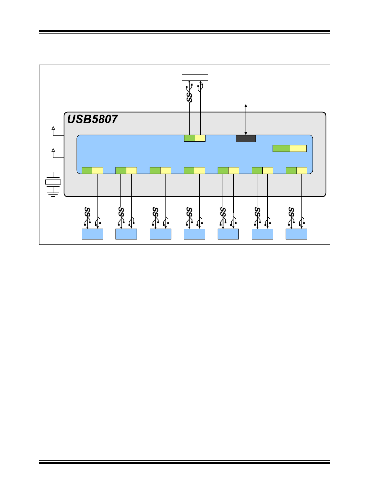
The Microchip USB5807 hub is a low-power, OEM configurable, USB 3.1 Gen 1 hub controller with 7 downstream ports
and advanced features for embedded USB applications. The USB5807 is fully compliant with the Universal Serial Bus
Revision 3.1 Specification and USB 2.0 Link Power Management Addendum. The USB5807 supports 5 Gbps Super-
Speed (SS), 480 Mbps Hi-Speed (HS), 12 Mbps Full-Speed (FS), and 1.5 Mbps Low-Speed (LS) USB downstream
devices on all enabled downstream ports.
The USB5807 supports the legacy USB speeds (HS/FS/LS) through a dedicated USB 2.0 hub controller that is the cul-
mination of five generations of Microchip hub controller design and experience with proven reliability, interoperability,
and device compatibility. The SuperSpeed hub controller operates in parallel with the USB 2.0 hub controller, decoupling
the 5 Gbps SS data transfers from bottlenecks due to the slower USB 2.0 traffic.
The USB5807 enables OEMs to configure their system using “Configuration Straps.” These straps simplify the config-
uration process, assigning default values to USB 3.1 Gen 1 ports and GPIOs. OEMs can disable ports, enable battery
charging, and define GPIO functions as default assignments on power-up, removing the need for OTP or external SPI
ROM.
The USB5807 supports downstream battery charging via the integrated battery charger detection circuitry, which sup-
ports the USB-IF Battery Charging (BC1.2) detection method and most Apple devices. The USB5807 provides the bat-
tery charging handshake and supports the following USB-IF BC1.2 charging profiles:
• DCP: Dedicated Charging Port (Power brick with no data)
• CDP: Charging Downstream Port (1.5A with data)
• SDP: Standard Downstream Port (0.5A with data)
• Custom profiles loaded via SMBus or OTP
Additionally, the USB5807 includes many powerful and unique features such as:
FlexConnect, which provides flexible connectivity options. One of the USB5807’s downstream ports can be reconfig-
ured to become the upstream port, allowing master capable devices to control other devices on the hub.
PortSwap, which adds per-port programmability to USB differential-pair pin locations. PortSwap allows direct alignment
of USB signals (D+/D-) to connectors to avoid uneven trace length or crossing of the USB differential signals on the
PCB.
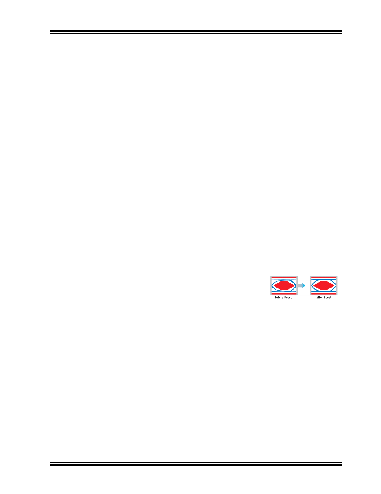
PHYBoost, which provides programmable levels of Hi-Speed USB signal drive strength
in the downstream port transceivers. PHYBoost attempts to restore USB signal integrity
in a compromised system environment. The graphic on the right shows an example of
Hi-Speed USB eye diagrams before and after PHYBoost signal integrity restoration. in
a compromised system environment.
VariSense, which controls the USB receiver sensitivity enabling programmable levels of USB signal receive sensitivity.
This capability allows operation in a sub-optimal system environment, such as when a captive USB cable is used.
Port Split, which allows for the USB3.1 Gen1 and USB2.0 portions of downstream ports 5 and 6 to operate inde-
pendently and enumerate two separate devices in parallel in special applications.
The USB5807 can be configured for operation through internal default settings. Custom OEM configurations are sup-
ported through external SPI ROM or OTP ROM. All port control signal pins are under firmware control in order to allow
for maximum operational flexibility, and are available as GPIOs for customer specific use.
The USB5807 is available in commercial (0°C to +70°C) and industrial (-40°C to +85°C) temperature ranges. An internal
block diagram of the USB5807 is shown in
Figure 2-1
.
USB5807
DS00002237D-page 7
2016-2018 Microchip Technology Inc.
FIGURE 2-1:
INTERNAL BLOCK DIAGRAM
Hub Controller Logic
I
2
C/SMB
I
2
C from Master
25 Mhz
USB3 USB2
P3
‘A’
AFE0
P4
‘A’
P5
‘A’
P6
‘A’
+3.3 V
+1.2 V
P1
‘A’
P2
‘A’
P0 ‘B’
P7
‘A’
AFE5
AFE4
AFE3
AFE2
AFE1
AFE3
AFE4
AFE5
AFE6
AFE2
AFE6
AFE1
AFE7
AFE7
AFE0
2016-2018 Microchip Technology Inc.
DS00002237D-page 8
USB5807
3.0
PIN DESCRIPTIONS
3.1
Pin Diagram
Note 1: Configuration straps are identified by an underlined symbol name. Signals that function as configuration
straps must be augmented with an external resistor when connected to a load. Refer to
Section 3.5, Con-
figuration Straps and Programmable Functions
FIGURE 3-1:
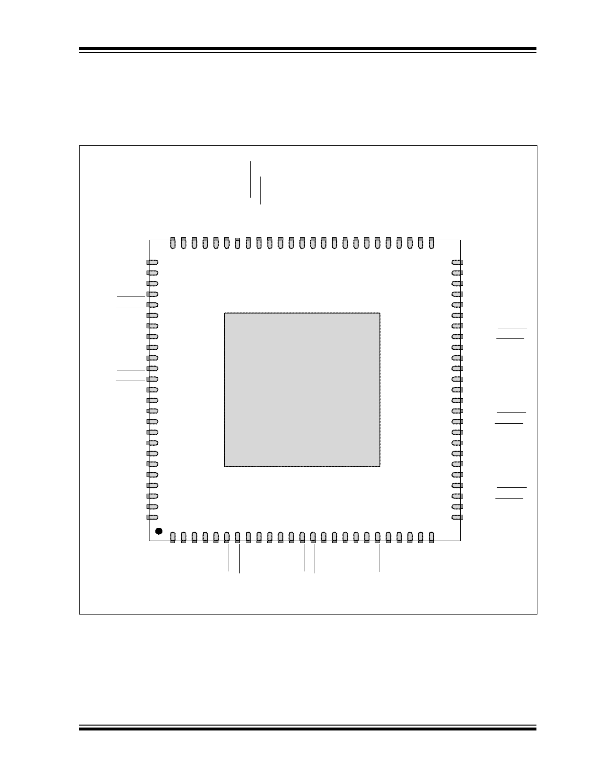
PIN ASSIGNMENTS (TOP VIEW)
100
99
98
97
96
95
94
93
92
90
89
88
87
86
85
91
16
15
14
13
12
11
10
9
8
6
5
4
3
2
1
7
41
40
39
37
36
35
34
33
32
31
30
29
28
27
26
75
74
73
72
71
70
68
67
66
65
69
64
63
62
61
60
38
RB
IA
S
XT
A
L
O
X
T
AL
I/
CL
K
IN
US
B
3DN_
R
XDM
1
US
B
3DN
_R
XDP1
V
DD1
2
US
B
3D
N
_T
XDM
1
US
B
3DN_
T
XDP1
US
B
2DN_
DM
1/
PR
T
_D
IS
_M
1
US
B
2DN
_D
P
1/
P
RT
_D
IS
_P
1
VDD33
USB2DN_DM4/PRT_DIS_M4
USB2DN_DP4/PRT_DIS_P4
USB3DN_TXDM4
USB3DN_TXDP4
USB2DN_DP3/PRT_DIS_P3
USB3DN_RXDM3
USB3DN_RXDP3
USB3DN_TXDM3
USB3DN_TXDP3
USB2DN_DM3/PRT_DIS_M3
VDD12
VDD12
S
P
E
E
D
_I
N
D
4/
B
C_
IND4
/G
P
IO
3
C_
AT
T
A
C
H
1/
G
P
IO
1
PR
T
_C
T
L
1/
G
P
IO
17
S
P
I_
CE
_N
/G
PI
O
7/
C
FG
_N
O
N
_R
E
M
S
P
I_
D
I/GP
IO9
/C
F
G
_B
C
_E
N
S
P
E
E
D_
IND6
/B
C_
IND6
/G
P
IO
66
SP
I_
DO
/C
_A
T
T
AC
H
2/
G
P
IO
5
SM
B
C
L
K
/G
P
IO
8
S
P
I_
CL
K
/C_
AT
T
A
C
H
3/
G
P
IO
4
GP
IO
69
SP
E
E
D
_I
N
D1
/B
C_
IND1
/G
P
IO
70
25
24
23
22
21
20
19
18
17
50
49
48
46
45
44
43
42
47
SPEED_IND5/BC_IND5/GPIO65
VDD12
59
58
57
56
55
54
53
52
51
PR
T
_C
T
L
6/
G
P
IO
22
SP
E
E
D
_I
N
D3
/B
C_
IND3
/G
P
IO
2
P
R
T_
C
T
L2
/G
P
IO
18
VDD
33
VDD3
3
S
P
E
E
D
_I
ND2
/B
C_
IND2
/G
P
IO
71
PR
T
_C
T
L
3/
G
P
IO
19
84
83
81
80
79
78
77
76
82
V
DD3
3
G
P
IO
12
/C
F
G
_S
T
RAP
USB3DN_RXDM4
USB3DN_RXDP4
VD
D1
2
C_ATTACH0/GPIO64
V
DD3
3
US
B
3DN_
R
XDM
2
US
B
3DN
_R
XDP2
V
DD1
2
US
B
3D
N
_T
XDM
2
US
B
3DN_
T
XDP2
US
B
2DN_
DM
2/
PR
T
_D
IS
_M
2
US
B
2DN
_D
P
2/
P
RT
_D
IS
_P
2
FLEX
_C
M
D
/G
P
IO
10
F
L
EX
_S
TA
T
E
/G
P
IO
72
TE
ST
EN
VB
U
S
_D
E
T
/G
P
IO
16
RE
SE
T
_N
SUSP_IND/GPIO68
VDD12
USB3DN_RXDM7
USB3DN_RXDP7
VDD12
USB3DN_TXDM7
USB3DN_TXDP7
USB2DN_DM7/PRT_DIS_M7
USB2DN_DP7/PRT_DIS_P7
USB3DN_RXDM6
USB3DN_RXDP6
VDD12
USB3DN_TXDM6
USB3DN_TXDP6
USB2DN_DM6/PRT_DIS_M6
USB2DN_DP6/PRT_DIS_P6
USB3UP_RXDM
USB3UP_RXDP
VDD12
USB3UP_TXDM
USB3UP_TXDP
USB2UP_DM
USB2UP_DP
VDD33
USB2DN_DM5/PRT_DIS_M5
USB2DN_DP5/PRT_DIS_P5
USB3DN_TXDM5
USB3DN_TXDP5
VDD12
USB3DN_RXDM5
USB3DN_RXDP5
VDD33
P
R
T_
C
T
L7
/GP
IO
23
SP
E
E
D_
IND7
/B
C_
IND7
/G
P
IO
67
VDD3
3
S
M
B
DAT
A/
G
P
IO
6
P
R
T_
C
T
L5
/G
P
IO
21
PR
T
_CT
L
4/
G
ANG
_P
W
R
/G
P
IO
20
thermal slug connects to VSS
Microchip
USB5807
(Top View 100-VQFN)
USB5807
DS00002237D-page 9
2016-2018 Microchip Technology Inc.
3.2
Pin Symbols
Pin Num.
Pin Name
Reset
Pin Num.
Pin Name
Reset
1
RBIAS
A/P
51
PRT_CTL6/GPIO22
PD-50k
2
VDD33
A/P
52
PRT_CTL5/GPIO21
PD-50k
3
XTALI/CLKIN
A/P
53
PRT_CTL7/GPIO23
PD-50k
4
XTALO
A/P
54
VDD33
A/P
5
VDD33
A/P
55
SPEED_IND7/BC_IND7/GPIO67
Z
6
USB2DN_DP1/PRT_DIS_P1
PD-15k
56
SPEED_IND3/BC_IND3/GPIO2
Z
7
USB2DN_DM1/PRT_DIS_M1
PD-15k
57
PRT_CTL4/GANG_PWR/GPIO20
PD-50k
8
USB3DN_TXDP1
Z
58
PRT_CTL3/GPIO19
PD-50k
9
USB3DN_TXDM1
Z
59
VDD12
A/P
10
VDD12
A/P
60
SPEED_IND4/BC_IND4/GPIO3
Z
11
USB3DN_RXDP1
Z
61
SPEED_IND2/BC_IND2/GPIO71
Z
12
USB3DN_RXDM1
Z
62
PRT_CTL2/GPIO18
PD-50k
13
USB2DN_DP2/PRT_DIS_P2
PD-15k
63
SPEED_IND1/BC_IND1/GPIO70
Z
14
USB2DN_DM2/PRT_DIS_M2
PD-15k
64
VDD33
A/P
15
USB3DN_TXDP2
Z
65
SPI_CLK/C_ATTACH3/GPIO4
Z
16
USB3DN_TXDM2
Z
66
SPI_DO/C_ATTACH2/GPIO5
PD-50k
17
VDD12
A/P
67
SPI_DI/GPIO9/CFG_BC_EN
Z
18
USB3DN_RXDP2
Z
68
SPI_CE_N/GPIO7/CFG_NON_REM
PU-50k
19
USB3DN_RXDM2
Z
69
GPIO69
Z
20
GPIO12/CFG_STRAP
Z
70
PRT_CTL1/GPIO17
PD-50k
21
FLEX_CMD/GPIO10
Z
71
SPEED_IND6/BC_IND6/GPIO66
Z
22
FLEX_STATE/GPIO72
Z
72
VDD33
A/P
23
TESTEN
Z
73
C_ATTACH1/GPIO1
Z
24
VBUS_DET/GPIO16
Z
74
SMBDATA/GPIO6
Z
25
RESET_N
R
75
SMBCLK/GPIO8
Z
26
VDD12
A/P
76
C_ATTACH0/GPIO64
Z
27
VDD33
A/P
77
SUSP_IND/GPIO68
Z
28
USB2DN_DP3/PRT_DIS_P3
PD-15k
78
VDD12
A/P
29
USB2DN_DM3/PRT_DIS_M3
PD-15k
79
USB2DN_DP7/PRT_DIS_P7
PD-15k
30
USB3DN_TXDP3
Z
80
USB2DN_DM7/PRT_DIS_M7
PD-15k
31
USB3DN_TXDM3
Z
81
USB3DN_TXDP7
Z
32
VDD12
A/P
82
USB3DN_TXDM7
Z
33
USB3DN_RXDP3
Z
83
VDD12
A/P
34
USB3DN_RXDM3
Z
84
USB3DN_RXDP7
Z
35
USB2DN_DP4/PRT_DIS_P4
PD-15k
85
USB3DN_RXDM7
Z
36
USB2DN_DM4/PRT_DIS_M4
PD-15k
86
USB2DN_DP6/PRT_DIS_P6
PD-15k
37
USB3DN_TXDP4
Z
87
USB2DN_DM6/PRT_DIS_M6
PD-15k
38
USB3DN_TXDM4
Z
88
USB3DN_TXDP6
Z
39
VDD12
A/P
89
USB3DN_TXDM6
Z
40
USB3DN_RXDP4
Z
90
VDD12
A/P
41
USB3DN_RXDM4
Z
91
USB3DN_RXDP6
Z
42
VDD33
A/P
92
USB3DN_RXDM6
Z
43
USB2DN_DP5/PRT_DIS_P5
PD-15k
93
VDD33
A/P
44
USB2DN_DM5/PRT_DIS_M5
PD-15k
94
USB2UP_DP
PD-1M
45
USB3DN_TXDP5
Z
95
USB2UP_DM
PD-1M
46
USB3DN_TXDM5
Z
96
USB3UP_TXDP
Z
47
VDD12
A/P
97
USB3UP_TXDM
Z
48
USB3DN_RXDP5
Z
98
VDD12
A/P
49
USB3DN_RXDM5
Z
99
USB3UP_RXDP
Z
50
SPEED_IND5/BC_IND5/GPIO65
Z
100
USB3UP_RXDM
Z
2016-2018 Microchip Technology Inc.
DS00002237D-page 10
USB5807
The pin reset state definitions are detailed in
Table 3-1
.
3.3
USB5807 Pin Descriptions
This section contains descriptions of the various USB5807 pins. The pin descriptions have been broken into functional
groups as follows:
•
USB 3.1 Gen 1 Pin Descriptions
•
USB 2.0 Pin Descriptions
•
Port Control Pin Descriptions
•
SPI Interface
•
USB Type-C Connector Controls
•
Miscellaneous Pin Descriptions
•
Configuration Strap Pin Descriptions
•
Power and Ground Pin Descriptions
The “_N” symbol in the signal name indicates that the active, or asserted, state occurs when the signal is at a low voltage
level. For example, RESET_N indicates that the reset signal is active low. When “_N” is not present after the signal
name, the signal is asserted when at the high voltage level.
The terms assertion and negation are used exclusively. This is done to avoid confusion when working with a mixture of
“active low” and “active high” signal. The term assert, or assertion, indicates that a signal is active, independent of
whether that level is represented by a high or low voltage. The term negate, or negation, indicates that a signal is inac-
tive.
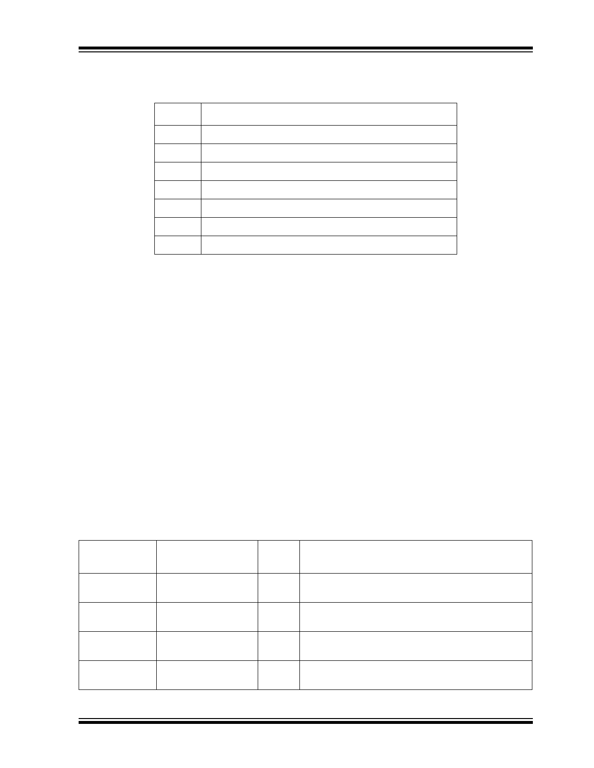
TABLE 3-1:
PIN RESET STATE LEGEND
Symbol
Description
A/P
Analog/Power Input
R
Reset Control Input
Z
Hardware disables output driver (high impedance)
PU-50k
Hardware enables internal 50kΩ pull-up
PD-50k
Hardware enables internal 50kΩ pull-down
PD-15k
Hardware enables internal 15kΩ pull-down
PD-1M
Hardware enables internal 1M pull-down
TABLE 3-2:
USB 3.1 GEN 1 PIN DESCRIPTIONS
Name
Symbol
Buffer
Type
Description
USB 3.1 Gen 1
Upstream D+ TX
USB3UP_TXDP
I/O-U
Upstream USB 3.1 Gen 1 Transmit Data Plus
USB 3.1 Gen 1
Upstream D- TX
USB3UP_TXDM
I/O-U
Upstream USB 3.1 Gen 1 Transmit Data Minus
USB 3.1 Gen 1
Upstream D+ RX
USB3UP_RXDP
I/O-U
Upstream USB 3.1 Gen 1 Receive Data Plus
USB 3.1 Gen 1
Upstream D- RX
USB3UP_RXDM
I/O-U
Upstream USB 3.1 Gen 1 Receive Data Minus