

2012 - 2015 Microchip Technology Inc.
DS00001682C-page 1
General Description
The USB5537B hub is a 7-port SuperSpeed/Hi-Speed,
low-power, configurable hub controller family fully com-
pliant with the USB 3.0 Specification. The USB5537B
supports 5 Gbps SuperSpeed (SS), 480 Mbps Hi-
Speed (HS), 12 Mbps Full-Speed (FS) and 1.5 Mbps
Low-Speed (LS) USB signaling for complete coverage
of all defined USB operating speeds.
The USB5537B supports USB 2.0 speeds through its
USB 2.0 hub controller. The new SuperSpeed hub con-
troller (available on 4 of the 7 ports) operates in parallel
with the USB 2.0 controller, so the 5 Gbps SuperSpeed
data transfers are not affected by the slower USB 2.0
traffic.
The USB5537B supports battery charging on a per port
basis. On battery charging enabled ports, the devices
provide automatic USB data line handshaking. The
handshaking supports USB 1.2 Charging Downstream
Port (CDP), Dedicated Charging Port (DCP) and non-
USB 1.2 devices.
The USB5537B is configured for operation through
internal default settings, where custom configurations
are supported through an on-chip OTP ROM, an exter-
nal SPI ROM, or SMBus.
Product Features
• USB 3.0 compliant 5 Gbps, 480 Mbps, 12 Mbps
and 1.5 Mbps operation, USB pins are 5 V toler-
ant
- Integrated termination and pull-up/pull-down
resistors
• Four downstream USB 3.0 ports
• Three additional USB 2.0 ports for use cases
where SS is not required
• Supports battery charging of most popular battery
powered devices
- USB-IF Battery Charging rev. 1.2 support
(DCP & CDP)
- Apple Portable product charger emulation
- Blackberry charger emulation
- Chinese YD/T 1591-2006 charger emulation
- Chinese YD/T 1591-2009 charger emulation
- Supports additional portable devices
• Emulates portable/handheld native wall chargers
- Charging profiles emulate a handheld
device’s wall charger to enable fast charging
(minutes vs. hours)
• Enables charging from a mobile platform that is
off
• Support tablets’ high current requirements
• Optimized for low-power operation and low ther-
mal dissipation
• Vendor Specific Messaging (VSM) support for
firmware upload over USB
• Configuration via OTP ROM, SPI ROM, or SMBus
• On-chip 8051 µC manages VBUS, and other hub
signals
• 8 KB RAM, 32 KB ROM
• One Time programmable (OTP) ROM: 8 kbit
- Includes on-chip charge pump
• Single 25 MHz XTAL or clock input for all on-chip
PLL and clocking requirements
• Supports JTAG boundary scan
• PHYBoost (USB 2.0)
- Selectable drive strength for improved signal
integrity
• VariSense (USB 2.0)
- controls the receiver sensitivity enabling four
programmable levels of USB signal receive
sensitivity
• IETF RFC 4122 compliant 128-bit UUID
Software Features
• Compatible with Microsoft Windows 7, Vista, XP,
Mac OSX10.4+, and Linux Hub Drivers
USB5537B
7-Port SS/HS USB Hub Controller

USB5537B
DS00001682C-page 2
2012 - 2015 Microchip Technology Inc.
TO OUR VALUED CUSTOMERS
It is our intention to provide our valued customers with the best documentation possible to ensure successful use of your Microchip
products. To this end, we will continue to improve our publications to better suit your needs. Our publications will be refined and
enhanced as new volumes and updates are introduced.
If you have any questions or comments regarding this publication, please contact the Marketing Communications Department via
E-mail at
docerrors@microchip.com
. We welcome your feedback.
Most Current Data Sheet
To obtain the most up-to-date version of this data sheet, please register at our Worldwide Web site at:
http://www.microchip.com
You can determine the version of a data sheet by examining its literature number found on the bottom outside corner of any page.
The last character of the literature number is the version number, (e.g., DS30000000A is version A of document DS30000000).
Errata
An errata sheet, describing minor operational differences from the data sheet and recommended workarounds, may exist for cur-
rent devices. As device/documentation issues become known to us, we will publish an errata sheet. The errata will specify the
revision of silicon and revision of document to which it applies.
To determine if an errata sheet exists for a particular device, please check with one of the following:
• Microchip’s Worldwide Web site;
http://www.microchip.com
• Your local Microchip sales office (see last page)
When contacting a sales office, please specify which device, revision of silicon and data sheet (include -literature number) you are
using.
Customer Notification System
Register on our web site at
www.microchip.com
to receive the most current information on all of our products.

2012 - 2015 Microchip Technology Inc.
DS00001682C-page 3
USB5537B
Table of Contents
1.0 Introduction ..................................................................................................................................................................................... 4
2.0 Block Diagram ................................................................................................................................................................................. 6
3.0 Pin Information ................................................................................................................................................................................ 7
4.0 Standard Interface Connections ................................................................................................................................................... 13
5.0 Functional Operation ..................................................................................................................................................................... 24
6.0 DC Parameters ............................................................................................................................................................................. 63
7.0 AC Specifications .......................................................................................................................................................................... 67
8.0 Package Drawing .......................................................................................................................................................................... 70
Appendix A: Data Sheet Revision History ........................................................................................................................................... 72
Appendix B: Acronyms ........................................................................................................................................................................ 74
Appendix C: References ..................................................................................................................................................................... 75
The Microchip Web Site ...................................................................................................................................................................... 76
Customer Change Notification Service ............................................................................................................................................... 76
Customer Support ............................................................................................................................................................................... 76
Product Identification System ............................................................................................................................................................. 77

USB5537B
DS00001682C-page 4
2012 - 2015 Microchip Technology Inc.
1.0
INTRODUCTION
1.1
Conventions
Within this manual, the following abbreviations and symbols are used to improve readability.
1.2
Overview
The USB5537B hub is a 7-port, low-power, configurable Hub Controller fully compliant with the USB 3.0 Specification
2.
The USB5537B supports 5 Gbps SuperSpeed (SS), 480 Mbps Hi-Speed (HS), 12 Mbps Full-Speed (FS) and
1.5 Mbps Low-Speed (LS) USB signaling for complete coverage of all defined USB operating speeds.
All required resistors on the USB ports are integrated into the hub. This includes all series termination resistors and all
required pull-down and pull-up resistors on D+ and D- pins. The over-current sense inputs for the downstream facing
ports have internal pull-up resistors.
The USB5537B hub includes programmable features such as:
• MultiTRAK
TM
Technology (USB 2.0): implements a dedicated Transaction Translator (TT) for each port. Dedi-
cated TTs help maintain consistent full-speed data throughput regardless of the number of active downstream
connections.
• PortSwap (USB 2.0): allows direct alignment of USB signals (D+/D-) to connectors to avoid uneven trace length
or crossing of the USB differential signals on the PCB.
• PHYBoost (USB 2.0): enables 4 programmable levels of USB signal drive strength in downstream port transceiv-
ers (HS, FS, LS USB only). PHYBoost will also attempt to restore USB signal integrity.
Example
Description
BIT
Name of a single bit within a field
FIELD.BIT
Name of a single bit (BIT) in FIELD
x…y
Range from x to y, inclusive
BITS[m:n]
Groups of bits from m to n, inclusive
PIN
Pin Name
zzzzb
Binary number (value zzzz)
0xzzz
Hexadecimal number (value zzz)
zzh
Hexadecimal number (value zz)
rsvd
Reserved memory location. Must write 0, read value indeterminate
code
Instruction code, or API function or parameter
Multi Word Name
Used for multiple words that are considered a single unit, such as:
Resource Allocate message, or Connection Label, or Decrement Stack Pointer instruction.
Section Name
Section or Document name.
x
Don’t care
<Parameter>
<> indicate a Parameter is optional or is only used under some conditions
{,Parameter}
Braces indicate Parameter(s) that repeat one or more times.
[Parameter]
Brackets indicate a nested Parameter. This Parameter is not real and actually decodes into
one or more real parameters.

2012 - 2015 Microchip Technology Inc.
DS00001682C-page 5
USB5537B
As shown on the
Product Identification System
page, three USB5537B firmware versions are available: “-5000”, “-6070”,
and “-6080”. These options differ in the following ways:
• The Dynamic Charging Port feature and related DYNCPDIS_N pin function are only available on the -6070 and -
6080 devices. Refer to
Section 5.1.3, "Dynamic Charging Port (6070 and 6080 Only)"
for additional details.
• The TRST/DYNCPDIS_N/UCS_SMBALERT_N pin buffer type is “IPU” in the -6070 and -6080 devices and “I” in
the -5000 device. Refer to
Pin Information on page 7
for additional details.
• The Global Suspend power consumption has been significantly lowered in the -6070 and -6080 device. Refer to
Section 6.3, "Power Consumption"
for additional details.
• The three USB 2.0 ports are configured as removable by default in the -6070 device. The three USB 2.0 ports are
configured as non-removable by default in the -5000 and -6080 devices.
1.3
Configurable Features
The USB5537B hub controller provides a default configuration that is sufficient for most applications. When initialized
in the default configuration, the following features may be configured:
• Downstream non-removable ports, where the hub will automatically report as a compound device
• Downstream disabled ports
• Downstream port power control and over-current detection on a ganged or individual basis
• USB signal drive strength
• USB differential pair pin location
The USB5537B hub controllers can alternatively be configured by OTP or as an SMBus slave device. When configured
by an OTP or over SMBus, the following configurable features are provided:
• Support for compound devices on a port-by-port basis
• Selectable over-current sensing and port power control on an individual or ganged basis to match the circuit board
component selection
• Customizable vendor ID, product ID, and device ID
• Configurable delay time for filtering the over-current sense inputs
• Indication of the maximum current that the hub consumes from the USB upstream port
• Indication of the maximum current required for the hub controller
• Custom string descriptors (up to 30 characters): Product, manufacturer, and serial number
Note:
At the time of this writing, products with a USB Host (or products such as docking stations with USB hubs
that must be submitted with an attached host enabled platform) are eligible for USB logo with a mixture of
USB2.0 and USB3.0 ports. An example of such a product is a dedicated docking station that can only be
used with a specific model or family of laptops. In this example, the docking station is submitted for USB
logo testing with a laptop and it is tested as a system. USB devices containing a hub with an exposed
upstream port that can be plugged into any host platform through USB cables and connectors (examples
are USB enabled monitors, printers, hard drives, etc.) are not eligible for logo with a mixture of USB 3.0
and USB 2.0 ports. These devices will need to consume the USB 2.0-only ports internally in order to be
eligible for a USB logo.
USB5537B
DS00001682C-page 6
2012 - 2015 Microchip Technology Inc.
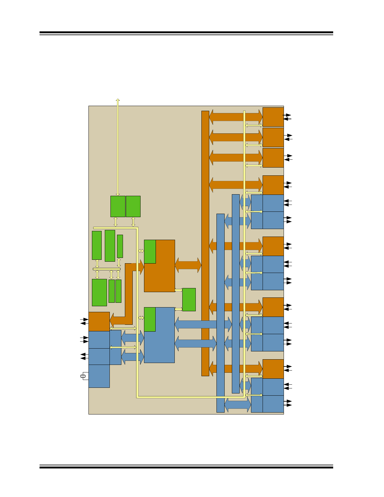
2.0
BLOCK DIAGRAM
FIGURE 2-1:
USB5537B BLOCK DIAGRAM
U
S
B
3
.0 H
u
b C
o
nt
ro
lle
r
TX
SS
PHY
RX
SS
PHY
USB
2
.0
PH
Y
USB 2.
0 Hu
b
C
o
n
tro
lle
r
Bu
ffe
r
HS/
F
S/
LS R
o
ut
in
g
L
o
g
ic
Co
mm
on
Bl
oc
k
& PLL
Re
gi
st
e
rs
&
H
u
b
I/O
VB
U
S
Con
tro
l
Bu
ffe
r
TX
SS
PH
Y
RX
SS
PH
Y
USB
2
.0
PH
Y
Bu
ffe
r
B
u
ffe
r
TX
SS
PHY
RX
SS
PH
Y
US
B
2
.0
PHY
B
u
ffe
r
Bu
ff
e
r
TX
SS
PH
Y
RX
SS
PHY
US
B2
.0
PH
Y
B
u
ffe
r
Bu
ffe
r
TX
SS
PHY
RX
SS
PHY
USB
2
.0
PH
Y
Bu
ffe
r
B
u
ffe
r
Up
stre
a
m
US
B P
o
rt
D
o
w
n
s
tr
e
a
m
US
B P
o
rt
1
D
owns
tre
a
m
US
B P
o
rt
2
D
ow
nst
re
a
m
U
S
B P
o
rt
3
D
o
w
ns
tr
e
a
m
USB
Po
rt
4
Embe
d
d
ed
80
51
µ
C
Re
g
ist
er
s
&
H
u
b I/O
32
k
R
O
M
8k
R
A
M
AP
B B
u
s
XD
at
a
XD
a
ta t
o
A
P
B Br
idg
e
D
o
wns
tre
am
RX
SS
bu
s
Do
wnst
re
am
TX S
S
bu
s
R
e
s
e
t &
80
51
Bo
ot
Se
q.
2k
OT
P
SP
I
Ma
ste
r
Tim
e
r
SP
I
US
B
2
.0
PH
Y
D
o
w
n
st
re
am
U
S
B 2
.0
Po
rt
s
5,
6,
& 7
USB
2
.0
PHY
US
B2
.0
PH
Y
2012 - 2015 Microchip Technology Inc.
DS00001682C-page 7
USB5537B
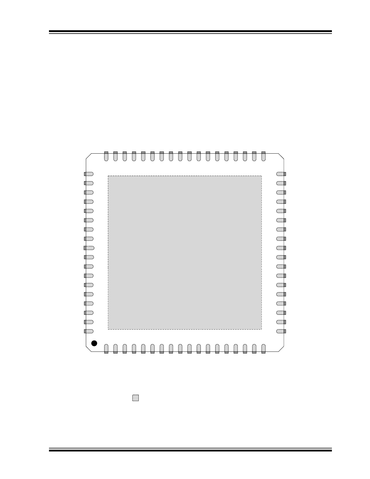
3.0
PIN INFORMATION
This chapter outlines the pinning configurations for each chip. The detailed pin descriptions are listed by function in
Sec-
tion 3.2, "Pin Descriptions (Grouped by Function)," on page 8
.
3.1
Pin Configurations
FIGURE 3-1:
USB5537B 72-PIN QFN
Ground Pad
(must be connected to VSS with a via field)
USB5537B
(Top View QFN-72)
USB
2
D
P
_D
N2
70
U
S
B
3
DM
_RXD
N2
69
U
S
B3
DP_RXD
N2
68
VD
D1
2
67
U
S
B3D
M
_
T
XD
N2
66
U
S
B
3
D
P
_
T
XD
N2
65
PRT
_
PW
R6/
P
R
T
_C
T
L
6
64
PRT
_
PW
R7/
P
R
T
_C
T
L
7
63
USB
2
DM_D
N1
62
U
S
B
3
DM
_RXD
N1
60
U
S
B3
DP_RXD
N1
59
VD
D1
2
58
U
S
B3D
M
_
T
XD
N1
57
U
S
B
3
D
P
_
T
XD
N1
56
55
USB
2
D
P
_D
N1
61
VD
D3
3
72
USB
2
DM_D
N2
71
USB2DM_DN5
16
USB2DP_DN5
15
USB2DM_DN4
14
USB2DP_DN4
13
USB3DM_RXDN4
12
USB3DP_RXDN4
11
VDD12
10
USB3DM_TXDN4
9
USB3DP_TXDN4
8
USB2DP_DN3
6
USB3DM_RXDN3
5
USB3DP_RXDN3
4
VDD12
3
USB3DM_TXDN3
2
USB3DP_TXDN3
1
USB2DM_DN3
7
TRST/D
YN
C
P
DIS_N
/
U
C
S_S
M
BALE
R
T
_N
17
TCK/
OCS1
18
P
R
T_P
W
R
2
/P
R
T
_C
TL2
36
P
R
T_P
W
R
1
/P
R
T
_C
TL1
35
34
33
SP
I_
D
I
32
SP
I_
D
O
31
SP
I_
C
L
K
30
SP
I_
C
E
_
N
29
VDD12
28
P
R
T_P
W
R
5
/P
R
T
_C
TL5/
SM
_
D
A
T
27
TEST
26
R
E
SET_N
25
TDI/OC
S3
24
TDO/
OCS4
23
TM
S
/OCS2
22
VD
D
3
3
21
PRT_PWR4/PRT_CTL4
20
P
R
T_P
W
R
3
/P
R
T
_C
TL3
19
VDD33
54
RBIAS
53
XTALIN/CLK_IN
52
XTALOUT
51
USB3DM_RXUP
50
USB3DP_RXUP
49
VDD12
48
USB3DM_TXUP
47
USB3DP_TXUP
46
USB2DM_UP
45
USB2DP_UP
44
USB2DP_DN7
43
USB2DM_DN7
42
USB2DP_DN6
41
USB2DM_DN6
40
VDD12
39
VB
U
S
38
VDD33
37
SM
_
C
LK
ATEST
VD
D1
2
Indicates pins on the bottom of the device.

USB5537B
DS00001682C-page 8
2012 - 2015 Microchip Technology Inc.
3.2
Pin Descriptions (Grouped by Function)
An N at the end of a signal name indicates that the active (asserted) state occurs when the signal is at a low voltage
level. When the N is not present, the signal is asserted when it is at a high voltage level. The terms assertion and nega-
tion are used exclusively in order to avoid confusion when working with a mixture of active low and active high signals.
The term assert, or assertion, indicates that a signal is active, independent of whether that level is represented by a high
or low voltage. The term negate, or negation, indicates that a signal is inactive.
TABLE 3-1:
USB5537B PIN DESCRIPTIONS
Symbol
Buffer Type
Description
USB 3.0 INTERFACE
USB3DP_TXUP
IO-U
USB 3 Upstream
Upstream SuperSpeed transmit data plus
USB3DM_TXUP
IO-U
USB 3 Upstream
Upstream SuperSpeed transmit data minus
USB3DP_RXUP
IO-U
USB 3 Upstream
Upstream SuperSpeed receive data plus
USB3DM_RXUP
IO-U
USB 3 Upstream
Upstream SuperSpeed receive data minus
USB3DP_TXDN[4:1]
IO-U
USB 3 Downstream
Downstream SuperSpeed transmit data plus for ports 1 through 4.
USB3DM_TXDN[4:1]
IO-U
USB 3 Downstream
Downstream SuperSpeed transmit data minus for ports 1 through 4.
USB3DP_RXDN[4:1]
IO-U
USB 3 Downstream
Downstream SuperSpeed receive data plus for ports 1 through 4.
USB3DM_RXDN[4:1]
IO-U
USB 3 Downstream
Downstream SuperSpeed receive data minus for ports 1 through 4.
USB 2.0 INTERFACE
USB2DP_UP
IO-U
USB Bus Data
These pins connect to the upstream USB bus data signals.
USB2DM_UP
IO-U
USB Bus Data
These pins connect to the upstream USB bus data signals.
USB2DP_DN[7:1]
IO-U
Hi-Speed USB Data
Downstream Hi-Speed data plus for ports 1 through 7.
USB2DM_DN[7:1]
IO-U
Hi-Speed USB Data
Downstream Hi-Speed data minus for ports 1 through 7.

2012 - 2015 Microchip Technology Inc.
DS00001682C-page 9
USB5537B
USB PORT CONTROL
PRT_PWR[7:1]/
PRT_CTL[7:1]
O12
USB Power Enable
Enables power to USB peripheral devices downstream.
Note:
This pin also provides configuration strap functions.
See
Note 3-1
.
VBUS
I
Upstream VBUS Power Detect
This pin can be used to detect the state of the upstream bus power. The
device monitors this pin to determine when to assert the internal D+ pull-
up resistor (signaling a connect event).
When designing a detachable hub, this pin should be connected to
VBUS on the upstream port via a 2:1 voltage divider. Two 100 k
resistors are suggested.
For self-powered applications with a permanently attached host, this pin
must be connected to a dedicated host control output, or connected to
the 3.3 V domain that powers the host (typically VDD33).
SPI INTERFACE
SPI_CE_N
O12
SPI Enable
SPI_CLK
O12
SPI Clock
SPI_DO
O12
SPI Serial Data Out
The output for the SPI port.
Note:
This pin also provides configuration strap functions.
See .
SPI_DI
I
SPI Serial Data In
The SPI data in to the controller from the ROM. This pin has a weak
internal pull-down applied at all times to prevent floating.
JTAG/OCS INTERFACE
TRST
IPU
(
Note 3-4
)
JTAG Asynchronous Reset
Note:
If using the SMBus interface, a pull-up on this signal will enable
Legacy Mode, while leaving it unconnected or pulled-down will
enable Advanced Mode.
DYNCPDIS_N
Dynamic Charging Port Disable
This active-low signal is used to globally disable charging port support.
Note:
This signal available in -6070 and -6080 versions only
UCS_SMBALERT_N
UCS1002 SMBus Alert
When charging port is enabled and SMBus devices are used, this signal
acts as an active-low SMBus alert.
TCK
I
JTAG Clock
This input is used for JTAG boundary scan and has a weak pull-down.
It can be left floating or grounded when not used. If the JTAG is
connected, then this signal will be detected high, and the software
disables the pull up after reset.
OCS1
Over-Current Sense 1
Input from external current monitor indicating an over-current condition.
Note:
This pin also provides configuration strap functions.
See
Note 3-3
.
TABLE 3-1:
USB5537B PIN DESCRIPTIONS (CONTINUED)
Symbol
Buffer Type
Description

USB5537B
DS00001682C-page 10
2012 - 2015 Microchip Technology Inc.
TMS
I
JTAG TMS
Used for JTAG boundary scan.
OCS2
Over-Current Sense 2
Input from external current monitor indicating an over-current condition.
Note:
This pin also provides configuration strap functions.
See
Note 3-3
.
TDI
I
JTAG TDI
Used for JTAG boundary scan.
OCS3
Over-Current Sense 3
Input from external current monitor indicating an over-current condition.
Note:
This pin also provides configuration strap functions.
See
Note 3-3
.
TDO
O12
JTAG TDO
Used for JTAG boundary scan.
OCS4
Over-Current Sense 4
Input from external current monitor indicating an over-current condition.
Note:
This pin also provides configuration strap functions.
See
Note 3-3
.
MISC
RESET_N
IS
Reset Input
The system uses this active low signal to reset the chip. The active low
pulse should be at least 1
s wide.
XTALIN
ICLKx
Crystal Input: 25 MHz crystal.
This pin connects to either one terminal of the crystal or to an external
25 MHz clock when a crystal is not used.
CLK_IN
External Clock Input
This pin connects to either one terminal of the crystal or to an external
25 MHz clock when a crystal is not used.
XTALOUT
OCLKx
Crystal Output
The clock output, providing a crystal 25 MHz. When an external clock
source is used to drive XTALIN/CLKIN, this pin becomes a no connect.
TEST
IPD
Test Pin
Treat as a no connect pin or connect to ground. No trace or signal
should be routed or attached to this pin.
RBIAS
I-R
USB Transceiver Bias
A12.0 k
(+/- 1%) resistor is attached from ground to this pin to set the
transceiver’s internal bias settings.
ATEST
A
Analog Test Pin
This signal is used for testing the chip and must always be connected
to ground.
SM_CLK
I/O12
SMBus Clock
SM_DAT
I/O12
SMBus Data Pin
Note:
This pin is MUXed with PRT_CTRL5
TABLE 3-1:
USB5537B PIN DESCRIPTIONS (CONTINUED)
Symbol
Buffer Type
Description