

2017 Microchip Technology Inc.
DS00002514A-page 1
Highlights
• Single-chip USB 2.0 Hi-Speed hub controller with
FlexConnect
- 1 upstream port for USB Host / OTG connection
- 4 downstream ports with FlexConnect capability on
all ports
• USB Battery Charging, revision 1.2, support on
downstream ports (DCP, CDP, SDP)
• Battery charging support for China and Apple
®
profiles
• USB to SMBus, I
2
S
™
, SPI, UART, and GPIO
- Apple authentication support
- I
2
S for audio support; Asynchronous In, Adaptive
Out, 48KHz, two channels, 16-bits/channel
- Flexible I
2
S capabilities with firmware update
Target Applications
• Media hubs
• Infotainment head units
• Automotive breakout boxes
• Docks
• Monitors
• Point of sale
• Host switch for diagnostic mode
• Host switch for field firmware upgrades
Product Features
• FlexConnect
- Downstream port able to swap with upstream port,
allowing USB host capable devices to control other
devices on the hub
• MultiTRAK
™
- Dedicated Transaction Translator per port
• PortMap
- Configurable port mapping and disable sequencing
• PortSwap
- Configurable differential intra-pair signal swapping
• PHYBoost
- Programmable USB transceiver drive strength for
recovering signal integrity
• VariSense
™
- Programmable USB receiver sensitivity
• USB Link Power Management (LPM) support
• Vendor Specific Messaging (VSM) support
• Architected for USB Power Delivery (PD) 3.0 sup-
port
- 32-bit embedded microcontroller in the hub exe-
cutes PD stack and system policy manager
- Interfaces to Microchip UPD350 Power Delivery
Interface device
- Power delivery stack runs from external SPI Flash
- SPI Flash provides flexibility for specification
revisions and evolving system needs
• Enhanced OEM configuration options available
through external straps, OTP configuration or
SMBus Slave port
• 3.3 V supply voltage
• AEC-Q100 compliance
- Microchip parts are tested to meet or exceed the
requirements of the AEC-Q100 automotive qualifi-
cation standards
• Packaging
- 48-pin VQFN (7 x 7 mm)
• Environmental
- Commercial temperature range (0°C to +70°C)
- Industrial temperature range (-40° to +85°C)
- Grade 3 Automotive temperature range
(-40° to +85°C)
USB4715
USB 2.0 Hi-Speed Hub Controller
with FlexConnect on all Ports

TO OUR VALUED CUSTOMERS
It is our intention to provide our valued customers with the best documentation possible to ensure successful use of your Microchip
products. To this end, we will continue to improve our publications to better suit your needs. Our publications will be refined and
enhanced as new volumes and updates are introduced.
If you have any questions or comments regarding this publication, please contact the Marketing Communications Department via
E-mail at
docerrors@microchip.com
. We welcome your feedback.
Most Current Data Sheet
To obtain the most up-to-date version of this data sheet, please register at our Worldwide Web site at:
http://www.microchip.com
You can determine the version of a data sheet by examining its literature number found on the bottom outside corner of any page.
The last character of the literature number is the version number, (e.g., DS30000000A is version A of document DS30000000).
Errata
An errata sheet, describing minor operational differences from the data sheet and recommended workarounds, may exist for cur-
rent devices. As device/documentation issues become known to us, we will publish an errata sheet. The errata will specify the
revision of silicon and revision of document to which it applies.
To determine if an errata sheet exists for a particular device, please check with one of the following:
• Microchip’s Worldwide Web site;
http://www.microchip.com
• Your local Microchip sales office (see last page)
When contacting a sales office, please specify which device, revision of silicon and data sheet (include -literature number) you are
using.
Customer Notification System
Register on our web site at
www.microchip.com
to receive the most current information on all of our products.
USB4715
DS00002514A-page 2
2017 Microchip Technology Inc.

2017 Microchip Technology Inc.
DS00002514A-page 3
USB4715
1.0
PREFACE
1.1
General Terms
TABLE 1-1:
GENERAL TERMS
Term
Description
ADC
Analog-to-Digital Converter
Byte
8 bits
CDC
Communication Device Class
EOP
End of Packet
EP
Endpoint
FIFO
First In First Out buffer
FS
Full-Speed
GPIO
General Purpose I/O
HS
Hi-Speed
Hub Feature Controller
The Hub Feature Controller, sometimes called a Hub Controller for short is the internal
processor used to enable the unique features of the USB Controller Hub. This is not to
be confused with the USB Hub Controller that is used to communicate the hub status
back to the Host during a USB session.
I
2
C
Inter-Integrated Circuit
LS
Low-Speed
lsb
Least Significant Bit
LSB
Least Significant Byte
msb
Most Significant Bit
MSB
Most Significant Byte
N/A
Not Applicable
NC
No Connect
OTP
One Time Programmable
PCB
Printed Circuit Board
PHY
Physical Layer
PLL
Phase Lock Loop
RESERVED
Refers to a reserved bit field or address. Unless otherwise noted, reserved bits must
always be zero for write operations. Unless otherwise noted, values are not guaran-
teed when reading reserved bits. Unless otherwise noted, do not read or write to
reserved addresses.
SDK
Software Development Kit
SMBus
System Management Bus
UUID
Universally Unique IDentifier
WORD
16 bits
USB4715
DS00002514A-page 4
2017 Microchip Technology Inc.
1.2
Buffer Types
TABLE 1-2:
BUFFER TYPE DESCRIPTIONS
Buffer
Description
1.3
Pin Reset States
The pin reset state definitions are detailed in
Table 1-3
. Refer to
Section 3.0, "Pin Descriptions and Configuration"
for
details on individual pin reset states.
TABLE 1-3:
PIN RESET STATE LEGEND
Symbol
Description
A/P
Analog/Power Input
Z
Hardware disables output driver (high impedance)
PD-15k
Hardware enables internal 15kΩ pull-down
PD-67k
Hardware enables internal 67kΩ pull-down
PU-67k
Hardware enables internal 67kΩ pull-up
USB
USB line
I
Input.
IS
Input with Schmitt trigger.
O4
Output buffer with 4mA sink and 4mA source.
O12
Output buffer with 12mA sink and 12mA source.
OD12
Open-drain output with 12mA sink.
PU
Internal pull-up. Unless otherwise noted in the pin description, internal pull-ups are
always enabled.
Internal pull-up resistors prevent unconnected inputs from floating. Do not rely on
internal resistors to drive signals external to the device. When connected to a load that
must be pulled high, an external resistor must be added.
PD
Internal pull-down. Unless otherwise noted in the pin description, internal pull-downs
are always enabled.
Internal pull-down resistors prevent unconnected inputs from floating. Do not rely on
internal resistors to drive signals external to the device. When connected to a load that
must be pulled low, an external resistor must be added.
ICLK
Crystal oscillator input pin.
OCLK
Crystal oscillator output pin.
I/O-U
Analog input/output defined in USB specification.
I-R
RBIAS.
A
Analog.
P
Power pin.

2017 Microchip Technology Inc.
DS00002514A-page 5
USB4715
1.4
Reference Documents
1.
Universal Serial Bus Revision 2.0 Specification
, http://www.usb.org
2.
AN2341 - USB4715 FlexConnect Operation, http://www.microchip.com
3.
AN2439 - Configuration of the USB491x/USB492x/USB4715
, http://www.microchip.com
4.
AN2437 - USB to GPIO Bridging with USB4715 and USB49xx
, http://www.microchip.com
5.
AN2438 - USB to I
2
C Bridging with USB4715 and USB49xx
, http://www.microchip.com
6.
AN2430 - USB to SPI Bridging with USB4715 and USB49xx
, http://www.microchip.com
7.
AN2426 - USB to UART Bridging with Microchip USB4715, USB4916, and USB4927
, http://www.microchip.com
8.
Battery Charging Specification
, Revision 1.2, Dec. 07, 2010, http://www.usb.org
9.
I
2
C-Bus Specification
, Version 1.1, http://www.nxp.com/documents/user_manual/UM10204.pdf
10. I
2
S-Bus Specification
, http://www.nxp.com/acrobat_download/various/I2SBUS.pdf
11. System Management Bus Specification, Version 1.0, http://smbus.org/specs
USB4715
DS00002514A-page 6
2017 Microchip Technology Inc.
2.0
INTRODUCTION
2.1
General Description
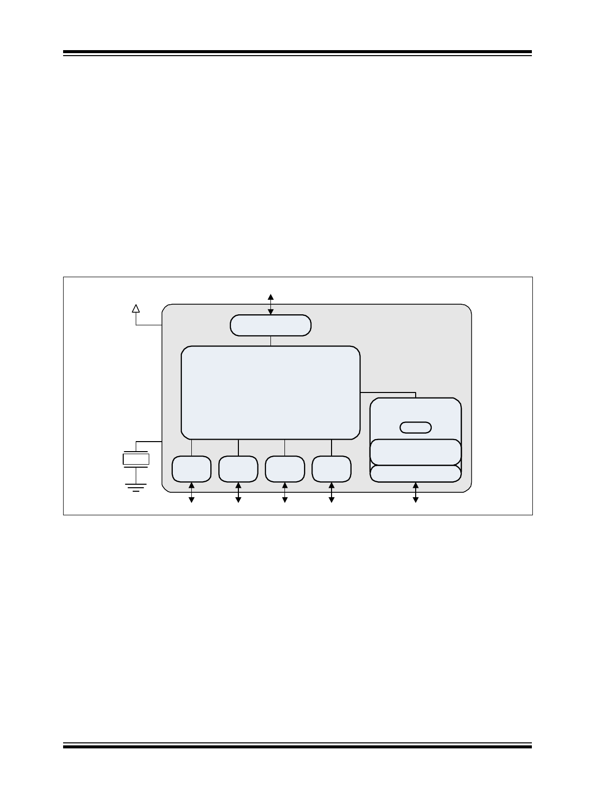
The Microchip USB4715 USB 2.0 Hi-Speed hub controller is a single-chip device targeted for automotive, industrial, and
commercial applications. Primary functions of the device include: multiple downstream USB ports supporting USB 2.0
Low Speed/Full Speed/Hi-Speed, single USB 2.0 Hi-Speed upstream connection to a USB host / OTG port, battery
charging support for BC1.2, Apple and China charging profiles, USB I/O bridging, and an on-chip microcontroller.
The USB4715 employs unique FlexConnect USB functionality, whereby one of the downstream ports can be reconfig-
ured to become an upstream port, allowing the host or master capability to be switched to equipment on any of the other
ports. This port/host becomes the master of the new USB bus, while the other ports can connect as USB devices, or
become dedicated charging ports.
The USB4715 is available in commercial (0°C to +70°C), industrial and Automotive Grade 3 (-40°C to +85°C) tempera-
ture ranges. An internal block diagram of the USB4715 is shown in
Figure 2-1
.
FIGURE 2-1:
INTERNAL BLOCK DIAGRAM
USB4715
25 MHz
3.3V
FlexHub Controller
Flex
Port 1
Flex
Port 2
Flex
Port 3
Flex
Port 4
USB
Flex USB 2.0
USB
USB
USB
Hub Feature
Controller
I/O Multiplexer
I
2
C/I
2
S/SPI/
UART/GPIO
OTP
I/O
USB Host / OTG Port 0
2017 Microchip Technology Inc.
DS00002514A-page 7
USB4715
3.0
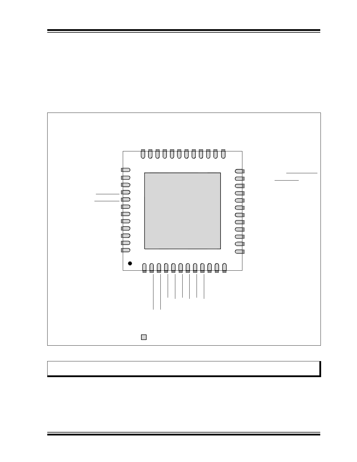
PIN DESCRIPTIONS AND CONFIGURATION
The pin assignments for the USB4715 are detailed in
Section 3.1, "USB4715 Pin Assignments"
. Pin descriptions are
provided in
Section 3.2, "Pin Descriptions"
.
3.1
USB4715 Pin Assignments
The device pin diagram for the USB4715 can be seen in
Figure 3-1
.
Table 3-1
provides a USB4715 pin assignments
table. Pin descriptions are provided in
Section 3.2, "Pin Descriptions"
.
FIGURE 3-1:
USB4715 PIN ASSIGNMENTS
CO
N
F
IG
_S
T
R
AP
_
2
F
L
E
X_U
S
B
_
D
P
1/
P
RT
_D
IS
_P
1
F
L
E
X_U
S
B
_
D
M
1
/P
R
T
_DI
S
_M
1
FL
E
X
_U
S
B
_
D
P
2/
P
R
T
_
D
IS
_
P
2
Ground Pad
(must be connected to VSS)
P
O
RT
_C
T
L
_
G
ANG
VD
DI
O
3
3
RE
S
E
T
_
N
F
L
E
X_U
S
B
_
D
M
2
/P
R
T
_DI
S
_M
2
CO
N
F
IG
_S
T
R
AP
_
1
VDDPLLREF33
RBIAS
XTALI/CLK_IN
XTALO
TESTEN/ATEST
USBH_DP0
FLEX_USB_DM3/PRT_DIS_M3
USBH_DM0
FLEX_USB_DP3/PRT_DIS_P3
VDDIO33
SPI_DI/SQI_D1/CFG_BC_EN
SPI_DO/SQI_D0
SPI_CLK/SQI_CLK
SPI_CE_N/SQI_CE_N/CFG_NON_REM
VDDIO33
PRT_CTL2/OCS2
PRT_CTL1/OCS1
PRT_CTL3/OCS3
VDDCR12
PROG_FUNC8
PROG_FUNC1
VD
DI
O
3
3
VD
DI
O
3
3
TEST1
TEST2
TEST3
VB
US
_
DE
T
F
L
E
X_U
S
B
_
D
M
4
/P
R
T
_DI
S
_M
4
P
R
T
_
C
TL4
/O
C
S
4
P
R
OG_
F
U
N
C
7
F
L
E
X_U
S
B
_
D
P
4/
P
RT
_D
IS
_P
4
SQ
I_
D
2
SQ
I_
D
3
P
RO
G
_
F
UN
C2
P
RO
G
_
F
UN
C3
P
RO
G
_
F
UN
C4
P
RO
G
_
F
UN
C5
P
RO
G
_
F
UN
C6
VD
DI
O
3
3
38
39
37
40
41
43
44
42
45
47
48
46
1
2
3
4
5
6
7
8
9
10
11
12
21
20
19
18
17
16
15
14
13
23
22
24
35
36
33
32
31
30
29
28
34
27
26
25
Microchip
USB4715
(Top View 48-VQFN)
Indicates pins on the bottom of the device.
Note:
Configuration straps are identified by an underlined symbol name. Signals that function as configuration
straps must be augmented with an external resistor when connected to a load.
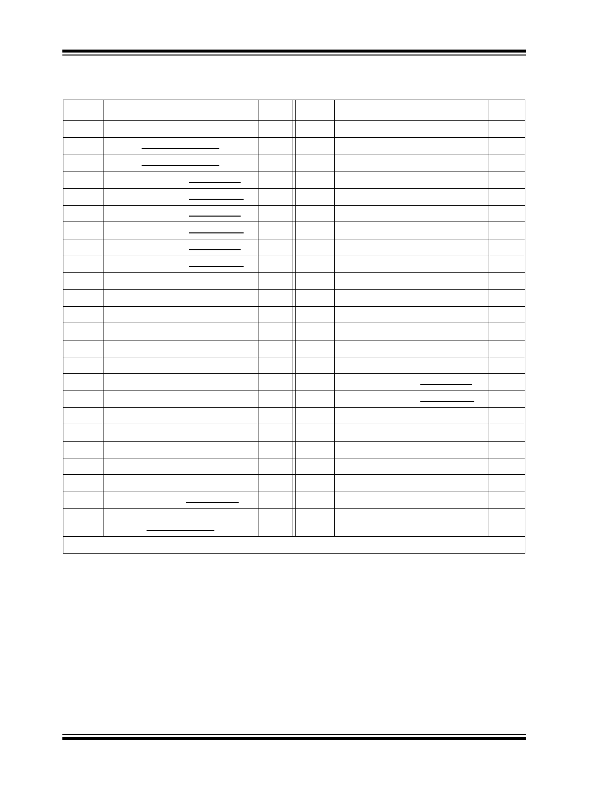
TABLE 3-1:
USB4715 PIN ASSIGNMENTS
Pin
Pin Name
Reset
Pin
Pin Name
Reset
1
PORT_CTL_GANG
PD-67k
25
VDDIO33
A/P
2
CONFIG_STRAP_1
Z
26
SQI_D2
Z
3
CONFIG_STRAP_2
Z
27
SQI_D3
Z
4
FLEX_USB_DP1/PRT_DIS_P1
PD-15k
28
PROG_FUNC6
Z
5
FLEX_USB_DM1/PRT_DIS_M1
PD-15k
29
PROG_FUNC5
Z
6
FLEX_USB_DP2/PRT_DIS_P2
PD-15k
30
PROG_FUNC4
Z
7
FLEX_USB_DM2/PRT_DIS_M2
PD-15k
31
VDDIO33
A/P
8
FLEX_USB_DP4/PRT_DIS_P4
PD-15k
32
PROG_FUNC3
Z
9
FLEX_USB_DM4/PRT_DIS_M4
PD-15k
33
PROG_FUNC2
Z
10
PRT_CTL4/OCS4
PD-67k
34
RESET_N
PD-67k
11
PROG_FUNC7
PD-67k
35
VBUS_DET
Z
12
VDDIO33
A/P
36
VDDIO33
A/P
13
TEST1
Z
37
PROG_FUNC1
Z
14
TEST2
Z
38
PROG_FUNC8
Z
15
TEST3
Z
39
VDDIO33
A/P
16
PRT_CTL3/OCS3
PD-67k
40
FLEX_USB_DP3/PRT_DIS_P3
PD-15k
17
PRT_CTL2/OCS2
PD-67k
41
FLEX_USB_DM3/PRT_DIS_M3
PD-15k
18
PRT_CTL1/OCS1
PD-67k
42
USBH_DP0
USB
19
VDDCR12
A/P
43
USBH_DM0
USB
20
VDDIO33
A/P
44
TESTEN/ATEST
A/P
21
SPI_CLK/SQI_CLK
Z
45
XTALO
A/P
22
SPI_DO/SQI_D0
PD-67k
46
XTALI/CLK_IN
A/P
23
SPI_DI/SQI_D1/CFG_BC_EN
Z
47
VDDPLLREF33
A/P
24
SPI_CE_N/SQI_CE_N/
CFG_NON_REM
PU-67k
48
RBIAS
A/P
Exposed Pad (VSS) must be connected to ground.
USB4715
DS00002514A-page 8
2017 Microchip Technology Inc.

2017 Microchip Technology Inc.
DS00002514A-page 9
USB4715
3.2
Pin Descriptions
TABLE 3-2:
PIN DESCRIPTIONS
Name
Symbol
Buffer
Type
Description
USB Interface
USB Upstream
D+
USBH_DP0
I/O-U
Upstream USB 2.0 Data Plus (D+)
USB Upstream
D-
USBH_DM0
I/O-U
Upstream USB 2.0 Data Minus (D-)
USB
Downstream
Ports 4-1 D+
FLEX_USB_DP[4:1]
I/O-U
Downstream USB 2.0 Ports 4-1 Data Plus (D+)
USB
Downstream
Ports 4-1 D-
FLEX_USB_DM[4:1]
I/O-U
Downstream USB 2.0 Ports 4-1 Data Minus (D-)
USB Port Control Pins
USB Ports 4-1
Power Enable
PRT_CTL[4:1]
I/O12
When the downstream port is enabled, this pin is set as
an input with an internal pull-up resistor applied. The
internal pull-up enables power to the downstream port
while the pin monitors for an active low overcurrent sig-
nal assertion from an external current monitor on USB
port 4. This pin will change to an output and be driven
low when the port is disabled by configuration or by the
host control.
USB Ports 4-1
Overcurrent
Sense
OCS[4:1]
I/O12
Overcurrent sense for ports 4-1.
Gang Power
PRT_CTL_GANG
I/O12
This pin becomes the port control pin for all downstream
ports when the hub is configured for ganged port power
control mode. All port power controllers are controlled
from this pin when the hub is configured for ganged port
power mode.
SPI Interface Pins
SPI Clock
SPI_CLK
I/O4
SPI clock.
SPI Data Out
SPI_DO
I/O4
SPI output data. If the SPI interface is enabled, this sig-
nal is the data out for the SPI port.
SPI Data In
SPI_DI
I/O4
SPI input data. If the SPI interface is enabled, this signal
must have a weak pull-down applied at all times to pre-
vent floating.
Note:
If SPI interface is not utilized, this pin cannot
be left floating. It must be connected per the
CFG_BC_EN pin description.
USB4715
DS00002514A-page 10
2017 Microchip Technology Inc.
SPI Chip
Enable
SPI_CE_EN
I/O4
Active low SPI chip enable input. If the SPI interface is
enabled, this pin must be driven high in powerdown
states.
Note:
If SPI interface is not utilized, this pin cannot
be left floating. It must be connected per the
CFG_NON_REM pin description.
SQI Interface Pins
SQI Clock
SQI_CLK
I/O4
SQI clock.
SQI Data 0-3
SQI_D[0:3]
I/O4
SQI Data 0-3. If the SQI interface is enabled, these sig-
nals function as Data 0 through 3.
SQI Chip
Enable
SQI_CE_EN
I/O4
Active low SQI chip enable input. If the SQI interface is
enabled, this pin requires an external pull-up resistor.
Note:
If SQI interface is not utilized, this pin cannot
be left floating. It must be connected per the
CFG_NON_REM pin description.
Miscellaneous
Programmable
Functions 8-1
PROG_FUNC[8:1]
I/O12
These selectable function pins can be assigned a role
via the CONFIG_STRAP_[2:1] pins, OTP configuration,
or SMBus configuration. Refer to
Section 3.3.4,
"PROG_FUNC[8:1] Configuration (CON-
FIG_STRAP_[2:1])"
for additional information.
VBUS
Detection
VBUS_DET
I
This signal detects the state of the upstream bus power.
When designing a detachable hub, this pin must be con-
nected to the VBUS power pin of the upstream USB port
through a resistor divider (50 k
Ω
by 100 k
Ω
) to provide
3.3 V.
For self-powered applications with a permanently
attached host, this pin must be connected to either 3.3 V
or 5.0 V through a resistor divider to provide 3.3 V.
In embedded applications, VBUS_DET may be con-
trolled (toggled) when the host desires to renegotiate a
connection without requiring a full reset of the device.
Reset Input
RESET_N
I
This active low signal is used by the system to reset the
device. The active low pulse should be at least 1
s
wide.
Bias Resistor
RBIAS
I-R
A 12.0 k
1.0% resistor is attached from ground to this
pin to set the transceiver’s internal bias settings. Place
the resistor as close to the device as possible with a
dedicated, low impedance connection to the GND plane.
External 25 MHz
Crystal Input
XTALI
ICLK
External 25 MHz crystal input.
TABLE 3-2:
PIN DESCRIPTIONS (CONTINUED)
Name
Symbol
Buffer
Type
Description