
2011 - 2014 Microchip Technology Inc.
DS00001824A-page 1
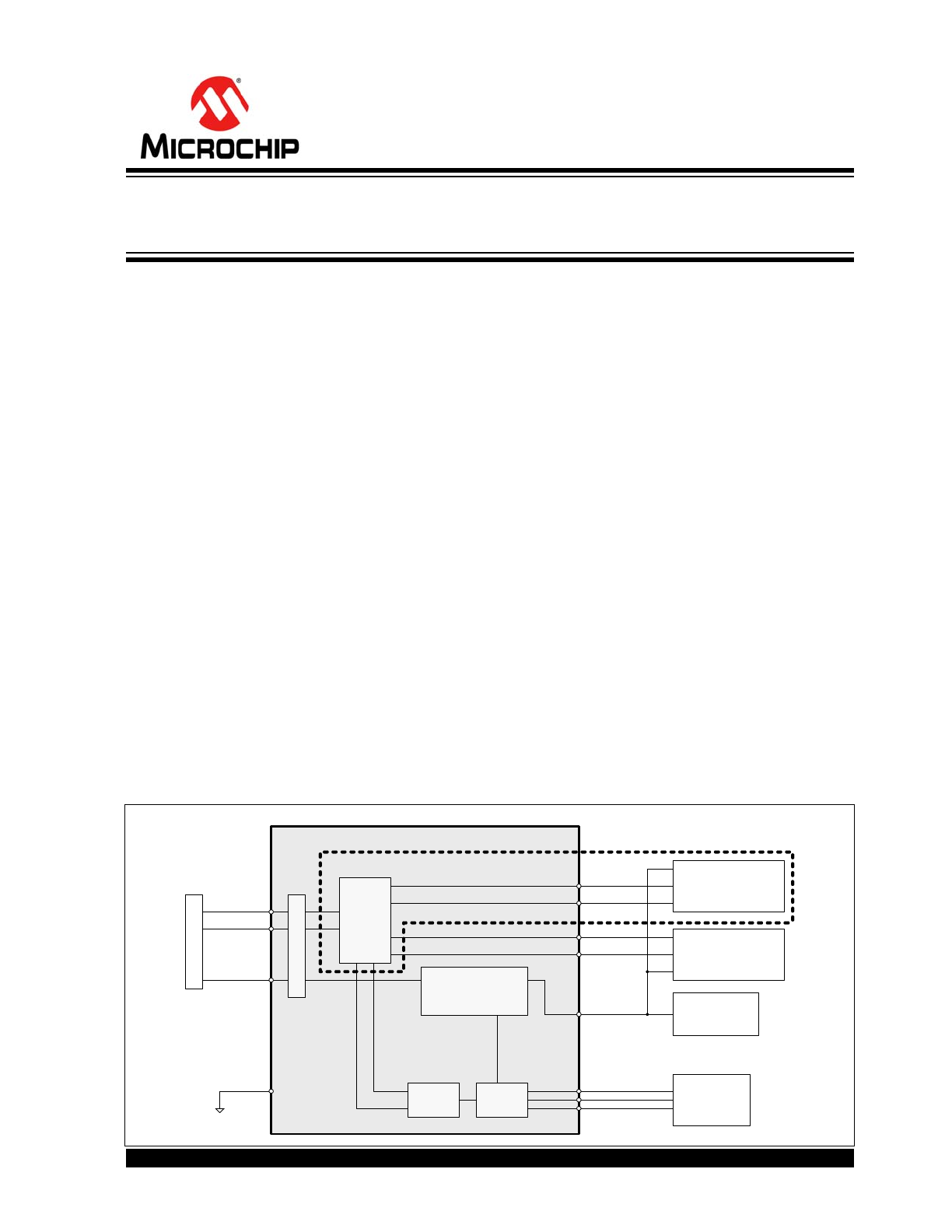
Features
• VBUS Over-Voltage Protection
- Protects internal circuits from VBUS up to 9V
- Over-Voltage/Under-Voltage Lockout opens
VBUS switch
- Interrupt to indicate Over-Voltage/Under-Volt-
age Lockout
- Integrated Low R
DSON
FET
• USB Port ESD Protection (DP/DM/VBUS)
- ±15kV (air discharge)
- ±15kV (contact discharge)
- IEC 61000-4-2 level 4 ESD protection without
external devices
• High Speed USB Mux for multiplexing the USB
lanes between different functions (USB3750 only)
- Switch the USB connector between two dif-
ferent functions
- High bandwidth USB switch passes HS USB
signals
• Provides USB Battery Charger Detection for:
- USB-IF Battery Charging compliant Dedi-
cated Charging Ports (DCP)
- USB-IF Battery Charging compliant Charging
Downstream Port (CDP)
- Standard Downstream Port (SDP); i.e. USB
host or downstream hub port
- Dedicated SE1 type chargers
• Dead Battery Provision Support (USB375x-1
only)
- Allows 100 mA trickle charging from VBUS
when attached to a Standard Downstream
Port (SDP) while not enumerated
- Built-in 100mA current limiting option
• Microchip RapidCharge Anywhere™ Provides:
- 3-times the charging current through a USB
port over traditional solutions
- USB-IF Battery Charging 1.2 compliance to
any portable device
- Charging current up to 1.5Amps via compati-
ble USB host or dedicated charger
- Dedicated Charging Port (DCP), Charging
(CDP) & Standard (SDP) Downstream Port
support
• flexPWR
®
Technology
- Extremely low current design ideal for battery
powered applications
- Maximizes power delivered to the system
• Industrial Operating Temperature -40°C to +85°C
• 16-Pin QFN RoHS compliant package; (3.0 mm x
3.0 mm x 0.9 mm height
USB375x Block Diagram
SCL
SDA
VBUS
VOUT
I
2
C
Interface
INT_B
DP
DM
ES
D
Pr
ote
c
ti
o
n
HS USB
Switch
DM_2
DP_2
U
S
B Co
n
necto
r
USB 2.0 PHY,
Processor, or
Accessory
Processor
Charger
Detection
Battery
Charger/
PMU
GND
DM_1
DP_1
USB 2.0 PHY,
Processor, or
Accessory
Over-Voltage/Under-Voltage
Protection and Current
Limiting
DP
DM
VBUS
VBUS
DP
DM
VBUS
DP
DM
HS Switch is USB3750 feature only
USB375x
USB 2.0 Protection IC with Battery
Charger Detection

USB375x
DS00001824A-page 2
2011 - 2014 Microchip Technology Inc.
TO OUR VALUED CUSTOMERS
It is our intention to provide our valued customers with the best documentation possible to ensure successful use of your Microchip
products. To this end, we will continue to improve our publications to better suit your needs. Our publications will be refined and
enhanced as new volumes and updates are introduced.
If you have any questions or comments regarding this publication, please contact the Marketing Communications Department via
E-mail at
docerrors@microchip.com
. We welcome your feedback.
Most Current Data Sheet
To obtain the most up-to-date version of this data sheet, please register at our Worldwide Web site at:
http://www.microchip.com
You can determine the version of a data sheet by examining its literature number found on the bottom outside corner of any page.
The last character of the literature number is the version number, (e.g., DS30000000A is version A of document DS30000000).
Errata
An errata sheet, describing minor operational differences from the data sheet and recommended workarounds, may exist for cur-
rent devices. As device/documentation issues become known to us, we will publish an errata sheet. The errata will specify the
revision of silicon and revision of document to which it applies.
To determine if an errata sheet exists for a particular device, please check with one of the following:
• Microchip’s Worldwide Web site;
http://www.microchip.com
• Your local Microchip sales office (see last page)
When contacting a sales office, please specify which device, revision of silicon and data sheet (include -literature number) you are
using.
Customer Notification System
Register on our web site at
www.microchip.com
to receive the most current information on all of our products.

2011 - 2014 Microchip Technology Inc.
DS00001824A-page 3
USB375x
Table of Contents
1.0 Introduction ..................................................................................................................................................................................... 4
2.0 Pin Layout ....................................................................................................................................................................................... 5
3.0 Electrical Specifications .................................................................................................................................................................. 7
4.0 General Operation ........................................................................................................................................................................ 12
5.0 Application Notes .......................................................................................................................................................................... 22
6.0 Package Information ..................................................................................................................................................................... 25
Appendix A: Data Sheet Revision History ........................................................................................................................................... 27
The Microchip Web Site ...................................................................................................................................................................... 28
Customer Change Notification Service ............................................................................................................................................... 28
Customer Support ............................................................................................................................................................................... 28
Product Identification System ............................................................................................................................................................. 29

USB375x
DS00001824A-page 4
2011 - 2014 Microchip Technology Inc.
1.0
INTRODUCTION
The USB375x integrates many features that have historically been discrete devices in a mobile product. This device
provides significant VBUS protection for the entire system, robust USB interface ESD protection, a USB 2.0 compliant
High Speed switch, and USB-IF Battery Charger Detection (revision 1.2) capabilities that are essential to the latest
mobile products.
Several advanced features allow the USB375x to be optimized for portable applications and to reduce both eBOM part
count and printed circuit board (PCB) area. Outstanding ESD robustness eliminates the need for external ESD protec-
tion devices.
In addition to the integrated ESD protection on the USB interface, the USB375x provides VBUS Over-Voltage Protection
(OVP).
The USB375x integrated battery charger detection circuitry supports USB-IF Battery Charger Detection. Battery charger
detection will begin automatically whenever VBUS rises above the UVLO threshold, and can also be completed manu-
ally through the I
2
C interface. The USB375x can detect a range of USB battery chargers including a Standard Down-
stream Port (SDP), a Charging Downstream Port (CDP), and a Dedicated Charging Port (DCP). For more information
on USB battery charger detection, please see the USB Battery Charging Specification, Revision 1.2 (
Note 1
).
The I
2
C interface gives processor control over the USB Switch, charger detection, OVLO settings, and status of the
USB375x. In addition, custom charger detection can be implemented through the I
2
C interface.
The USB375x family is enabled with Microchip's RapidCharge Anywhere
TM
which supports USB-IF Battery Charging
1.2 for any portable device (
Note 1
). RapidCharge Anywhere
TM
provides three times the charging current through a
USB port over traditional solutions which translate up to 1.5 amps via compatible USB host or dedicated charger. In
addition, this provides a complete USB charging ecosystem between device and host ports such as Dedicated Charging
Port (DCP), Charging (CDP) and Standard (SDP) Downstream Ports.
1.1
Reference Documents
• Universal Serial Bus Specification, Revision 2.0
• USB Battery Charging Specification, Revision 1.2 (
Note 1
)
Note 1: The device’s Data Contact Detect Timeout parameter does not conform to the USB Battery Charging Spec-
ification. However, this will not affect other factors in charger detection. Refer to
Table 3-2, “Electrical Spec-
ifications,” on page 7
for additional information.
2011 - 2014 Microchip Technology Inc.
DS00001824A-page 5
USB375x
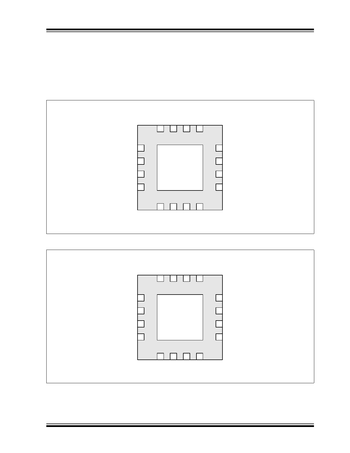
2.0
PIN LAYOUT
2.1
Pin Diagram
The USB375x is available in a QFN (3 x 3 mm) package. The USB3750 pin diagram is detailed in
Figure 2-1
. The
USB3751 pin diagram is detailed in
Figure 2-2
.
FIGURE 2-1:
QFN PACKAGE DIAGRAM (USB3750)
FIGURE 2-2:
QFN PACKAGE DIAGRAM (USB3751)
VBUS
DP_1
VBUS
DM_2
VOUT
VOUT
VOUT
DM_
1
DP_
2
DP
GN
D
IN
T
_
B
DM
VBUS
SC
L
SD
A
1
2
3
4
5
6
7
8
12
11
10
9
16
15
14
13
VBUS
DP_1
VBUS
NC
VOUT
VOUT
VOUT
DM_
1
NC
DP
GN
D
IN
T
_
B
DM
VBUS
SC
L
SD
A
1
2
3
4
5
6
7
8
12
11
10
9
16
15
14
13

USB375x
DS00001824A-page 6
2011 - 2014 Microchip Technology Inc.
2.2
Pin Definitions
The following table details the ball/pin definitions for the package diagrams above.
Pin
Name
Type/
Direction
Description
15
DP
Analog
USB Mux Output
14
DM
Analog
1
DP_1
Analog
USB Mux Input 1
16
DM_1
Analog
13
DP_2 / NC
Analog
USB Mux Input 2 (USB3750 Only)
These pins are No Connects for the USB3751 (do not connect)
12
DM_2 / NC
Analog
8
GND
Analog
Ground. The QFN package flag should also connected to ground.
6
SCL
Input
I
2
C Clock input. This pin is an open drain output and requires a
10Kohm pull-up.
5
SDA
Open Drain/
IO
Bi-Directional I
2
C data. This pin is an open drain output and
requires a 10Kohm pull-up.
7
INT_B
Open Drain/
Output
Open Drain Interrupt. This pin is an open drain output that is
pulled low when an interrupt occurs. A 10Kohm pull-up is required
on this pin.
9
VOUT
Analog
Overvoltage switch output. This pin is connected to VBUS when
the overvoltage protection switch is enabled. It is also the output
of the 100mA current limit.
The three VOUT pins must be connected together. When VBUS
is between UVLO and OVLO VOUT is connected to VBUS. When
VBUS is below UVLO or above OVLO the USB375x will tri-state.
10
11
2
VBUS
Analog
VBUS pin of the USB connector.
The three VBUS pins must be connected together. When the
OVP switch is closed, the VBUS pin will be isolated from VOUT.
When the OVP switch is open, VBUS will be connected to VOUT.
The USB375x is powered from this pin.
3
4
2011 - 2014 Microchip Technology Inc.
DS00001824A-page 7
USB375x
3.0
ELECTRICAL SPECIFICATIONS
3.1
Absolute Maximum Ratings
Stresses beyond the Absolute Maximum Ratings may damage the USB375x.
3.2
Electrical Specifications
TABLE 3-1:
ABSOLUTE MAXIMUM RATINGS
Description
Rating
Unit
VBUS Voltage to GND
-0.3 to 9.0
V
VOUT Voltage to GND
-0.3 to 7.5
V
Any other pin to GND
-0.3 to 5.5
V
Operating Temperature Range
-40 to +85
C
Storage Temperature Range
-55 to +150
C
ESD Rating
HBM
8,000
V
IEC-61000-4-2
15,000 (Air)
15,000 (Contact)
V
ESD Rating (SDA, SCL, INT_B)
HBM
1,500
V
TABLE 3-2:
ELECTRICAL SPECIFICATIONS
Characteristic
Symbol
MIN
TYP
MAX
Units
Conditions
V
VBUS
= 5.0V, T
A
= -40C to 85C, all typical values at T
A
= 27C unless otherwise noted.
VBUS Characteristics
VBUS Operating range
V
VBUS
2
9
V
VBUS Over Voltage Lockout
(USB3750 Only)
V
OVLO
6.2
6.9
V
USB3750 Only
VBUS Over Voltage Lockout
(USB3751 Only)
V
OVLO
5.45
6.15
V
USB3751 Only
VBUS Under Voltage Lockout
V
UVLO
3.3
3.4
3.8
V
VBUS Over Voltage Hysteresis
V
OVLO
100
mV
VBUS Under Voltage Hysteresis V
UVLO
100
mV
Operating Current
(OVP open)
I
DD_OFF
110
uA
V
VBUS
< V
UVLO
Operating Current
(OVP closed)
I
DD_ON
75
115
370
uA
V
UVLO
< V
VBUS
< V
OVLO
Operating Current
(100mA Limit enabled)
I
DD
150
185
480
uA
V
UVLO
< V
VBUS
< V
OVLO
VBUS Switch Characteristics
Overvoltage Switch ON
Resistance
R
ON_VBUS
70
mohm
QFN package
Overvoltage Switch Current
1.8
A
V
UVLO
< V
VBUS
< V
OVLO
Overvoltage Switch OFF
Leakage
I
OFF_VBUS
1
uA
VBUS = 5.0V; VOUT = 0V
VBUS Resistance to Ground
R
VBUS
100
Kohm
VBUS Capacitance
C
VBUS
1.0
uF
Charger Detection Characteristics 4.4 < VBUS < 5.5V
DP and DM leakage
1
uA
0.0V < Vpin < 3.3V
Data Source Voltage
V
DAT_SRC
0.5
0.7
V
I
DAT_SRC
> 250uA
Data Detect Voltage
V
DAT_REF
0.25
0.4
V
USB375x
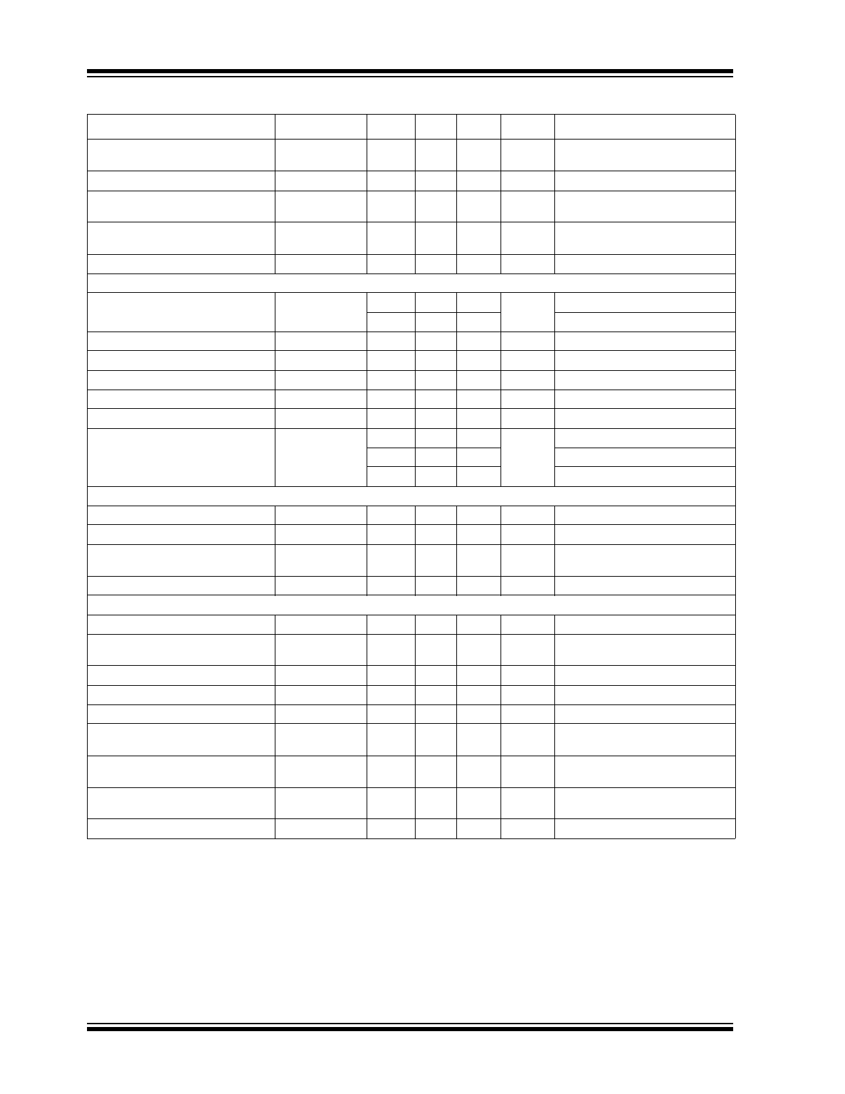
DS00001824A-page 8
2011 - 2014 Microchip Technology Inc.
Note 1: The device’s Data Contact Detect Timeout (T
DCD_TOUT
) parameter does not conform to the USB Battery
Charging Specification’s T
DCD_TOUT
minimum of 300 ms. However, this will not affect other factors in char-
ger detection.
Data Connect Detect Current
Source
I
DP_SRC
7
13
uA
Data Sink Current
I
DAT_SINK
50
150
uA
DP/DM Single Ended RX
Threshold
V
SE_RX
0.8
1.95
V
4.75V < VBUS < 5.25V
SE1 High Current Charger RX
Threshold
V
SE_RXH
2.1
2.56
V
4.75V < VBUS < 5.25V
DP/DM Pull Down Resistors
R
PD
14.25
24.8
Kohm
USB Mux Characteristics (USB3750 Only)
USB Mux On Resistance
R
ON_USB
10
ohm
0V < Vin < 3.3V
2.5
0V < Vin < 0.4V
USB Mux Off Leakage
I
OFF_USB
0.85
uA
0V < Vin < 3.3V
On Capacitance
C
ON_USB
9
pF
Off Capacitance
C
OFF_USB
6.5
pF
Off Isolation
-35
dB
R
L
= 50 ohm, F = 250MHz
Crosstalk
-40
dB
R
L
= 50 ohm, F = 250MHz
Bandwidth (-3dB)
BW
1000
MHz
R
L
= 50 ohm, C
L
= 0pF
800
R
L
= 50 ohm, C
L
= 5pF
500
R
L
= 50 ohm, C
L
= 10pF
Control Signal Characteristics
Input Logic High Threshold
V
IN_H
1.4
V
VBUS > UVLO
Input Logic Low Threshold
V
IN_L
0.4
V
VBUS > UVLO
Output Drive Strength
V
OUT_L
0.4
V
VBUS > UVLO, 4.0mA sink
current
Control Signal Leakage Current
1
nA
0 < Vpin < VOUT
Timing Characteristics
Clock Accuracy
T
CLK
0.5
1
2
ms
Oscillator Accuracy
Soft POR Reset Time
T
SOFT_POR
20
ms
Time to autoclear Soft POR.
UVLO and OVLO Release Timer T
VLO_ RELEASE
3
6.5
ms
UVLO and OVLO Engage Time T
VLO_ ENGAGE
0.5
1.7
ms
Data Contact Detect Timeout
T
DCD_TOUT
40
150
ms
See
Note 1
Vdat_src and Idat_sink Enable
Time
T
VDPSRC_ON
40
80
160
ms
Delay from Vdat_det to OVP
switch enable
T
VDPSRC_HICR
NT
40
80
160
ms
SE1 Charger Detection wait for
SE1 timer
T
CD_SE1
40
80
160
ms
Interrupt Self Clear Timer
T
INT
0.5
1
2
ms
TABLE 3-2:
ELECTRICAL SPECIFICATIONS (CONTINUED)
Characteristic
Symbol
MIN
TYP
MAX
Units
Conditions
2011 - 2014 Microchip Technology Inc.
DS00001824A-page 9
USB375x
3.3
Timing Diagrams
3.3.1
UVLO AND OVLO TIMING
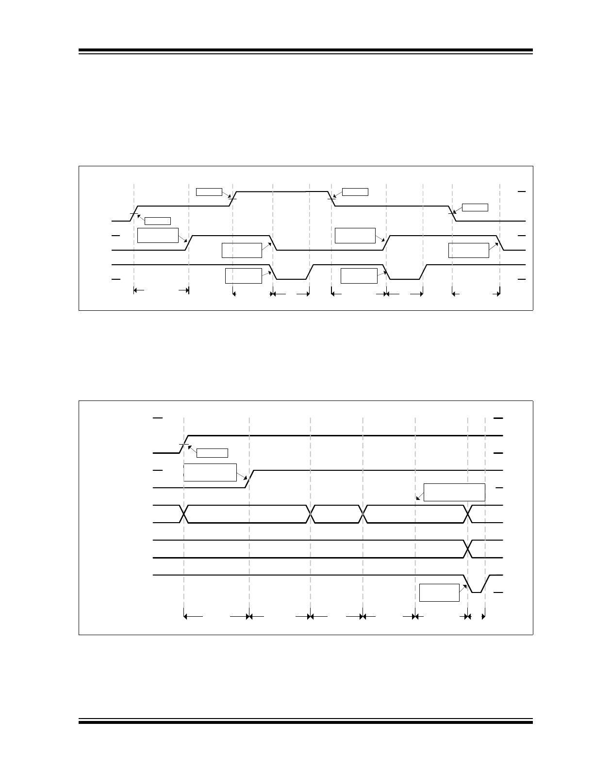
The timing diagram below shows the operation of the OVP switch as VBUS crosses the UVLO and OVLO thresholds.
The behavior of the INT_B signal is also shown in
Figure 3-1
below.
3.3.2
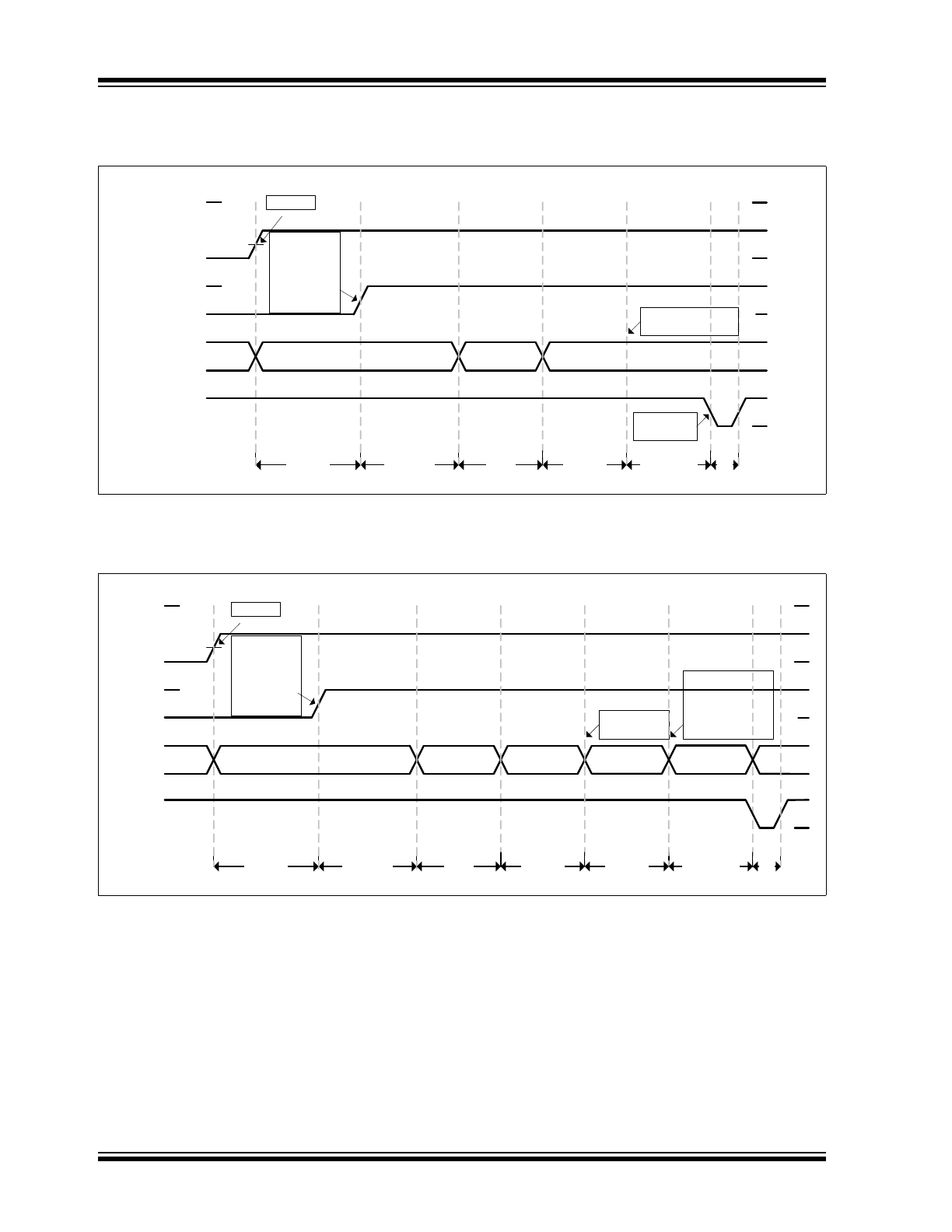
AUTOMATIC CHARGER DETECTION TIMING
The timing diagrams below illustrate the automatic charger detection timing that is followed when implementing the
automatic charger detection flow charts shown in this section.
FIGURE 3-1:
UVLO AND OVLO TIMING
FIGURE 3-2:
CHARGER DETECTION TIMING SDP (USB3750-1)
INT_B
VBUS
T
VLO_RELEASE
VOUT
OVLO
UVLO
T
VLO_ENGAGE
OVP switch
enabled
OVP switch
disabled
OVLO
Fall Int.
UVLO
T
VLO_ENGAGE
OVLO
Start Chrg
Detection
OVP switch
disabled
OVLO Int.
T
VLO_RELEASE
T
INT
T
INT
VBUS
T
VLO_Release
Con. Det. or
T
DCD_TOUT
UVLO
VOUT
OVP Switch
Enable
Chrg Det
Finish
T
VDPSRC_ON
USB
X
Connect Detect
Check for SE1
T
CD_SE1
Drive Vdat Source on DP
USB Mux
T
VDPSRC_HICRNT
INT_B
T
INT
Mux1 and Mux2 Disabled
Mux1 En.
V
DatDet
=0
SDP Detected
Mux1 En.
USB375x
DS00001824A-page 10
2011 - 2014 Microchip Technology Inc.
FIGURE 3-3:
CHARGER DETECTION TIMING SDP (USB3751-X)
FIGURE 3-4:
CHARGER DETECTION TIMING DCP OR CDP (USB3751-X)
VBUS
T
VLO_Release
Con. Det. or
T
DCD_TOUT
UVLO
VOUT
Chrg Det
Finish
T
VDPSRC_ON
USB
X
Connect Detect
Check for SE1
T
CD_SE1
Drive Vdat Source on DP
T
VDPSRC_HICRNT
INT_B
T
INT
V
DatDet
=0
SDP Detected
OVP Switch
Enable
(USB3750-2)/
100mA
Current Limit
Enable
(USB3750-1)
VBUS
T
VLO_Release
Con. Det. or
T
DCD_TOUT
UVLO
VOUT
V
DatDet
= 1
T
VDPSRC_ON
USB
X
Connect Detect
Check for SE1
T
CD_SE1
Drive Vdat
Source on DP
T
VDPSRC_HICRNT
INT_B
T
INT
Drive Vdat
Source on DM
T
VDPSRC_ON
USB Tri-State
USB
Pass-Thru
If V
DatDet
= 0
CDP detected
If V
DatDet
= 1
DCP detected
OVP Switch
Enable
(USB3750-2)/
100mA
Current limit
Enable
(USB3750-1)
2011 - 2014 Microchip Technology Inc.
DS00001824A-page 1
Features
• VBUS Over-Voltage Protection
- Protects internal circuits from VBUS up to 9V
- Over-Voltage/Under-Voltage Lockout opens
VBUS switch
- Interrupt to indicate Over-Voltage/Under-Volt-
age Lockout
- Integrated Low R
DSON
FET
• USB Port ESD Protection (DP/DM/VBUS)
- ±15kV (air discharge)
- ±15kV (contact discharge)
- IEC 61000-4-2 level 4 ESD protection without
external devices
• High Speed USB Mux for multiplexing the USB
lanes between different functions (USB3750 only)
- Switch the USB connector between two dif-
ferent functions
- High bandwidth USB switch passes HS USB
signals
• Provides USB Battery Charger Detection for:
- USB-IF Battery Charging compliant Dedi-
cated Charging Ports (DCP)
- USB-IF Battery Charging compliant Charging
Downstream Port (CDP)
- Standard Downstream Port (SDP); i.e. USB
host or downstream hub port
- Dedicated SE1 type chargers
• Dead Battery Provision Support (USB375x-1
only)
- Allows 100 mA trickle charging from VBUS
when attached to a Standard Downstream
Port (SDP) while not enumerated
- Built-in 100mA current limiting option
• Microchip RapidCharge Anywhere™ Provides:
- 3-times the charging current through a USB
port over traditional solutions
- USB-IF Battery Charging 1.2 compliance to
any portable device
- Charging current up to 1.5Amps via compati-
ble USB host or dedicated charger
- Dedicated Charging Port (DCP), Charging
(CDP) & Standard (SDP) Downstream Port
support
• flexPWR
®
Technology
- Extremely low current design ideal for battery
powered applications
- Maximizes power delivered to the system
• Industrial Operating Temperature -40°C to +85°C
• 16-Pin QFN RoHS compliant package; (3.0 mm x
3.0 mm x 0.9 mm height
USB375x Block Diagram
SCL
SDA
VBUS
VOUT
I
2
C
Interface
INT_B
DP
DM
ES
D
Pr
ote
c
ti
o
n
HS USB
Switch
DM_2
DP_2
U
S
B Co
n
necto
r
USB 2.0 PHY,
Processor, or
Accessory
Processor
Charger
Detection
Battery
Charger/
PMU
GND
DM_1
DP_1
USB 2.0 PHY,
Processor, or
Accessory
Over-Voltage/Under-Voltage
Protection and Current
Limiting
DP
DM
VBUS
VBUS
DP
DM
VBUS
DP
DM
HS Switch is USB3750 feature only
USB375x
USB 2.0 Protection IC with Battery
Charger Detection
USB375x
DS00001824A-page 2
2011 - 2014 Microchip Technology Inc.
TO OUR VALUED CUSTOMERS
It is our intention to provide our valued customers with the best documentation possible to ensure successful use of your Microchip
products. To this end, we will continue to improve our publications to better suit your needs. Our publications will be refined and
enhanced as new volumes and updates are introduced.
If you have any questions or comments regarding this publication, please contact the Marketing Communications Department via
E-mail at
docerrors@microchip.com
. We welcome your feedback.
Most Current Data Sheet
To obtain the most up-to-date version of this data sheet, please register at our Worldwide Web site at:
http://www.microchip.com
You can determine the version of a data sheet by examining its literature number found on the bottom outside corner of any page.
The last character of the literature number is the version number, (e.g., DS30000000A is version A of document DS30000000).
Errata
An errata sheet, describing minor operational differences from the data sheet and recommended workarounds, may exist for cur-
rent devices. As device/documentation issues become known to us, we will publish an errata sheet. The errata will specify the
revision of silicon and revision of document to which it applies.
To determine if an errata sheet exists for a particular device, please check with one of the following:
• Microchip’s Worldwide Web site;
http://www.microchip.com
• Your local Microchip sales office (see last page)
When contacting a sales office, please specify which device, revision of silicon and data sheet (include -literature number) you are
using.
Customer Notification System
Register on our web site at
www.microchip.com
to receive the most current information on all of our products.
2011 - 2014 Microchip Technology Inc.
DS00001824A-page 3
USB375x
Table of Contents
1.0 Introduction ..................................................................................................................................................................................... 4
2.0 Pin Layout ....................................................................................................................................................................................... 5
3.0 Electrical Specifications .................................................................................................................................................................. 7
4.0 General Operation ........................................................................................................................................................................ 12
5.0 Application Notes .......................................................................................................................................................................... 22
6.0 Package Information ..................................................................................................................................................................... 25
Appendix A: Data Sheet Revision History ........................................................................................................................................... 27
The Microchip Web Site ...................................................................................................................................................................... 28
Customer Change Notification Service ............................................................................................................................................... 28
Customer Support ............................................................................................................................................................................... 28
Product Identification System ............................................................................................................................................................. 29
USB375x
DS00001824A-page 4
2011 - 2014 Microchip Technology Inc.
1.0
INTRODUCTION
The USB375x integrates many features that have historically been discrete devices in a mobile product. This device
provides significant VBUS protection for the entire system, robust USB interface ESD protection, a USB 2.0 compliant
High Speed switch, and USB-IF Battery Charger Detection (revision 1.2) capabilities that are essential to the latest
mobile products.
Several advanced features allow the USB375x to be optimized for portable applications and to reduce both eBOM part
count and printed circuit board (PCB) area. Outstanding ESD robustness eliminates the need for external ESD protec-
tion devices.
In addition to the integrated ESD protection on the USB interface, the USB375x provides VBUS Over-Voltage Protection
(OVP).
The USB375x integrated battery charger detection circuitry supports USB-IF Battery Charger Detection. Battery charger
detection will begin automatically whenever VBUS rises above the UVLO threshold, and can also be completed manu-
ally through the I
2
C interface. The USB375x can detect a range of USB battery chargers including a Standard Down-
stream Port (SDP), a Charging Downstream Port (CDP), and a Dedicated Charging Port (DCP). For more information
on USB battery charger detection, please see the USB Battery Charging Specification, Revision 1.2 (
Note 1
).
The I
2
C interface gives processor control over the USB Switch, charger detection, OVLO settings, and status of the
USB375x. In addition, custom charger detection can be implemented through the I
2
C interface.
The USB375x family is enabled with Microchip's RapidCharge Anywhere
TM
which supports USB-IF Battery Charging
1.2 for any portable device (
Note 1
). RapidCharge Anywhere
TM
provides three times the charging current through a
USB port over traditional solutions which translate up to 1.5 amps via compatible USB host or dedicated charger. In
addition, this provides a complete USB charging ecosystem between device and host ports such as Dedicated Charging
Port (DCP), Charging (CDP) and Standard (SDP) Downstream Ports.
1.1
Reference Documents
• Universal Serial Bus Specification, Revision 2.0
• USB Battery Charging Specification, Revision 1.2 (
Note 1
)
Note 1: The device’s Data Contact Detect Timeout parameter does not conform to the USB Battery Charging Spec-
ification. However, this will not affect other factors in charger detection. Refer to
Table 3-2, “Electrical Spec-
ifications,” on page 7
for additional information.
2011 - 2014 Microchip Technology Inc.
DS00001824A-page 5
USB375x
2.0
PIN LAYOUT
2.1
Pin Diagram
The USB375x is available in a QFN (3 x 3 mm) package. The USB3750 pin diagram is detailed in
Figure 2-1
. The
USB3751 pin diagram is detailed in
Figure 2-2
.
FIGURE 2-1:
QFN PACKAGE DIAGRAM (USB3750)
FIGURE 2-2:
QFN PACKAGE DIAGRAM (USB3751)
VBUS
DP_1
VBUS
DM_2
VOUT
VOUT
VOUT
DM_
1
DP_
2
DP
GN
D
IN
T
_
B
DM
VBUS
SC
L
SD
A
1
2
3
4
5
6
7
8
12
11
10
9
16
15
14
13
VBUS
DP_1
VBUS
NC
VOUT
VOUT
VOUT
DM_
1
NC
DP
GN
D
IN
T
_
B
DM
VBUS
SC
L
SD
A
1
2
3
4
5
6
7
8
12
11
10
9
16
15
14
13
USB375x
DS00001824A-page 6
2011 - 2014 Microchip Technology Inc.
2.2
Pin Definitions
The following table details the ball/pin definitions for the package diagrams above.
Pin
Name
Type/
Direction
Description
15
DP
Analog
USB Mux Output
14
DM
Analog
1
DP_1
Analog
USB Mux Input 1
16
DM_1
Analog
13
DP_2 / NC
Analog
USB Mux Input 2 (USB3750 Only)
These pins are No Connects for the USB3751 (do not connect)
12
DM_2 / NC
Analog
8
GND
Analog
Ground. The QFN package flag should also connected to ground.
6
SCL
Input
I
2
C Clock input. This pin is an open drain output and requires a
10Kohm pull-up.
5
SDA
Open Drain/
IO
Bi-Directional I
2
C data. This pin is an open drain output and
requires a 10Kohm pull-up.
7
INT_B
Open Drain/
Output
Open Drain Interrupt. This pin is an open drain output that is
pulled low when an interrupt occurs. A 10Kohm pull-up is required
on this pin.
9
VOUT
Analog
Overvoltage switch output. This pin is connected to VBUS when
the overvoltage protection switch is enabled. It is also the output
of the 100mA current limit.
The three VOUT pins must be connected together. When VBUS
is between UVLO and OVLO VOUT is connected to VBUS. When
VBUS is below UVLO or above OVLO the USB375x will tri-state.
10
11
2
VBUS
Analog
VBUS pin of the USB connector.
The three VBUS pins must be connected together. When the
OVP switch is closed, the VBUS pin will be isolated from VOUT.
When the OVP switch is open, VBUS will be connected to VOUT.
The USB375x is powered from this pin.
3
4
2011 - 2014 Microchip Technology Inc.
DS00001824A-page 7
USB375x
3.0
ELECTRICAL SPECIFICATIONS
3.1
Absolute Maximum Ratings
Stresses beyond the Absolute Maximum Ratings may damage the USB375x.
3.2
Electrical Specifications
TABLE 3-1:
ABSOLUTE MAXIMUM RATINGS
Description
Rating
Unit
VBUS Voltage to GND
-0.3 to 9.0
V
VOUT Voltage to GND
-0.3 to 7.5
V
Any other pin to GND
-0.3 to 5.5
V
Operating Temperature Range
-40 to +85
C
Storage Temperature Range
-55 to +150
C
ESD Rating
HBM
8,000
V
IEC-61000-4-2
15,000 (Air)
15,000 (Contact)
V
ESD Rating (SDA, SCL, INT_B)
HBM
1,500
V
TABLE 3-2:
ELECTRICAL SPECIFICATIONS
Characteristic
Symbol
MIN
TYP
MAX
Units
Conditions
V
VBUS
= 5.0V, T
A
= -40C to 85C, all typical values at T
A
= 27C unless otherwise noted.
VBUS Characteristics
VBUS Operating range
V
VBUS
2
9
V
VBUS Over Voltage Lockout
(USB3750 Only)
V
OVLO
6.2
6.9
V
USB3750 Only
VBUS Over Voltage Lockout
(USB3751 Only)
V
OVLO
5.45
6.15
V
USB3751 Only
VBUS Under Voltage Lockout
V
UVLO
3.3
3.4
3.8
V
VBUS Over Voltage Hysteresis
V
OVLO
100
mV
VBUS Under Voltage Hysteresis V
UVLO
100
mV
Operating Current
(OVP open)
I
DD_OFF
110
uA
V
VBUS
< V
UVLO
Operating Current
(OVP closed)
I
DD_ON
75
115
370
uA
V
UVLO
< V
VBUS
< V
OVLO
Operating Current
(100mA Limit enabled)
I
DD
150
185
480
uA
V
UVLO
< V
VBUS
< V
OVLO
VBUS Switch Characteristics
Overvoltage Switch ON
Resistance
R
ON_VBUS
70
mohm
QFN package
Overvoltage Switch Current
1.8
A
V
UVLO
< V
VBUS
< V
OVLO
Overvoltage Switch OFF
Leakage
I
OFF_VBUS
1
uA
VBUS = 5.0V; VOUT = 0V
VBUS Resistance to Ground
R
VBUS
100
Kohm
VBUS Capacitance
C
VBUS
1.0
uF
Charger Detection Characteristics 4.4 < VBUS < 5.5V
DP and DM leakage
1
uA
0.0V < Vpin < 3.3V
Data Source Voltage
V
DAT_SRC
0.5
0.7
V
I
DAT_SRC
> 250uA
Data Detect Voltage
V
DAT_REF
0.25
0.4
V
USB375x
DS00001824A-page 8
2011 - 2014 Microchip Technology Inc.
Note 1: The device’s Data Contact Detect Timeout (T
DCD_TOUT
) parameter does not conform to the USB Battery
Charging Specification’s T
DCD_TOUT
minimum of 300 ms. However, this will not affect other factors in char-
ger detection.
Data Connect Detect Current
Source
I
DP_SRC
7
13
uA
Data Sink Current
I
DAT_SINK
50
150
uA
DP/DM Single Ended RX
Threshold
V
SE_RX
0.8
1.95
V
4.75V < VBUS < 5.25V
SE1 High Current Charger RX
Threshold
V
SE_RXH
2.1
2.56
V
4.75V < VBUS < 5.25V
DP/DM Pull Down Resistors
R
PD
14.25
24.8
Kohm
USB Mux Characteristics (USB3750 Only)
USB Mux On Resistance
R
ON_USB
10
ohm
0V < Vin < 3.3V
2.5
0V < Vin < 0.4V
USB Mux Off Leakage
I
OFF_USB
0.85
uA
0V < Vin < 3.3V
On Capacitance
C
ON_USB
9
pF
Off Capacitance
C
OFF_USB
6.5
pF
Off Isolation
-35
dB
R
L
= 50 ohm, F = 250MHz
Crosstalk
-40
dB
R
L
= 50 ohm, F = 250MHz
Bandwidth (-3dB)
BW
1000
MHz
R
L
= 50 ohm, C
L
= 0pF
800
R
L
= 50 ohm, C
L
= 5pF
500
R
L
= 50 ohm, C
L
= 10pF
Control Signal Characteristics
Input Logic High Threshold
V
IN_H
1.4
V
VBUS > UVLO
Input Logic Low Threshold
V
IN_L
0.4
V
VBUS > UVLO
Output Drive Strength
V
OUT_L
0.4
V
VBUS > UVLO, 4.0mA sink
current
Control Signal Leakage Current
1
nA
0 < Vpin < VOUT
Timing Characteristics
Clock Accuracy
T
CLK
0.5
1
2
ms
Oscillator Accuracy
Soft POR Reset Time
T
SOFT_POR
20
ms
Time to autoclear Soft POR.
UVLO and OVLO Release Timer T
VLO_ RELEASE
3
6.5
ms
UVLO and OVLO Engage Time T
VLO_ ENGAGE
0.5
1.7
ms
Data Contact Detect Timeout
T
DCD_TOUT
40
150
ms
See
Note 1
Vdat_src and Idat_sink Enable
Time
T
VDPSRC_ON
40
80
160
ms
Delay from Vdat_det to OVP
switch enable
T
VDPSRC_HICR
NT
40
80
160
ms
SE1 Charger Detection wait for
SE1 timer
T
CD_SE1
40
80
160
ms
Interrupt Self Clear Timer
T
INT
0.5
1
2
ms
TABLE 3-2:
ELECTRICAL SPECIFICATIONS (CONTINUED)
Characteristic
Symbol
MIN
TYP
MAX
Units
Conditions
2011 - 2014 Microchip Technology Inc.
DS00001824A-page 9
USB375x
3.3
Timing Diagrams
3.3.1
UVLO AND OVLO TIMING
The timing diagram below shows the operation of the OVP switch as VBUS crosses the UVLO and OVLO thresholds.
The behavior of the INT_B signal is also shown in
Figure 3-1
below.
3.3.2
AUTOMATIC CHARGER DETECTION TIMING
The timing diagrams below illustrate the automatic charger detection timing that is followed when implementing the
automatic charger detection flow charts shown in this section.
FIGURE 3-1:
UVLO AND OVLO TIMING
FIGURE 3-2:
CHARGER DETECTION TIMING SDP (USB3750-1)
INT_B
VBUS
T
VLO_RELEASE
VOUT
OVLO
UVLO
T
VLO_ENGAGE
OVP switch
enabled
OVP switch
disabled
OVLO
Fall Int.
UVLO
T
VLO_ENGAGE
OVLO
Start Chrg
Detection
OVP switch
disabled
OVLO Int.
T
VLO_RELEASE
T
INT
T
INT
VBUS
T
VLO_Release
Con. Det. or
T
DCD_TOUT
UVLO
VOUT
OVP Switch
Enable
Chrg Det
Finish
T
VDPSRC_ON
USB
X
Connect Detect
Check for SE1
T
CD_SE1
Drive Vdat Source on DP
USB Mux
T
VDPSRC_HICRNT
INT_B
T
INT
Mux1 and Mux2 Disabled
Mux1 En.
V
DatDet
=0
SDP Detected
Mux1 En.
USB375x
DS00001824A-page 10
2011 - 2014 Microchip Technology Inc.
FIGURE 3-3:
CHARGER DETECTION TIMING SDP (USB3751-X)
FIGURE 3-4:
CHARGER DETECTION TIMING DCP OR CDP (USB3751-X)
VBUS
T
VLO_Release
Con. Det. or
T
DCD_TOUT
UVLO
VOUT
Chrg Det
Finish
T
VDPSRC_ON
USB
X
Connect Detect
Check for SE1
T
CD_SE1
Drive Vdat Source on DP
T
VDPSRC_HICRNT
INT_B
T
INT
V
DatDet
=0
SDP Detected
OVP Switch
Enable
(USB3750-2)/
100mA
Current Limit
Enable
(USB3750-1)
VBUS
T
VLO_Release
Con. Det. or
T
DCD_TOUT
UVLO
VOUT
V
DatDet
= 1
T
VDPSRC_ON
USB
X
Connect Detect
Check for SE1
T
CD_SE1
Drive Vdat
Source on DP
T
VDPSRC_HICRNT
INT_B
T
INT
Drive Vdat
Source on DM
T
VDPSRC_ON
USB Tri-State
USB
Pass-Thru
If V
DatDet
= 0
CDP detected
If V
DatDet
= 1
DCP detected
OVP Switch
Enable
(USB3750-2)/
100mA
Current limit
Enable
(USB3750-1)