
2011 - 2015 Microchip Technology Inc.
DS00001725D-page 1
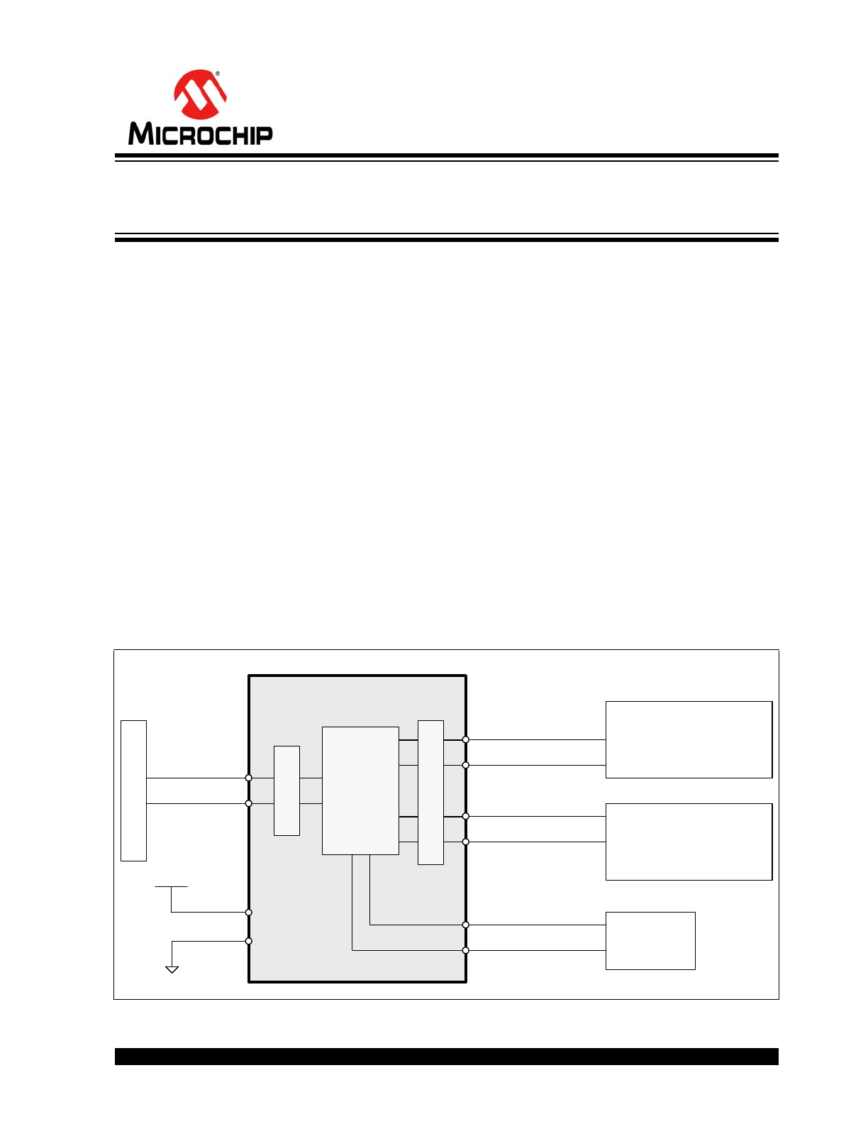
Features
• High Speed USB Mux for multiplexing the USB
lanes between different functions
- Switch the USB connector between two dif-
ferent functions
- Up to 1GHz Bandwidth
• USB Port ESD Protection (DP/DM)
- 8kV HBM
• flexPWR
TM
Technology
- 30nA Active/Standby Current
- Extremely low power design ideal for battery
powered applications
• Control inputs accommodate 1.8V to 5V inputs
• DP/DM tolerate up to 5.5V
• -40°C to +85°C Operating Temperature
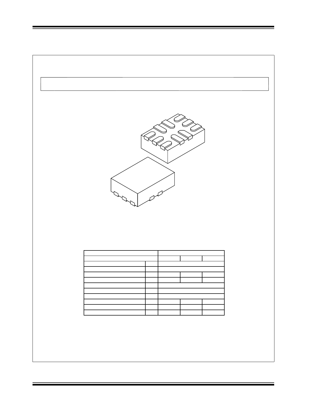
• 10-pin, QFN, RoHS compliant package;
(1.3mm x 1.8mm x 0.55mm height, 0.4mm pitch)
• 10-pin, QFN, RoHS compliant package;
(1.6mm x 2.1mm x 0.55mm height, 0.5mm pitch)
• Automotive option
Block Diagram
OE_N
S
DP
DM
ES
D
Pr
ot
ec
ti
o
n
HS USB
Switch
DM_2
DP_2
U
S
B Conn
ecto
r
USB 2.0 PHY,
Processor, or
Accessory
Processor
GND
DM_1
DP_1
USB 2.0 PHY,
Processor, or
Accessory
DP
DM
DP
DM
DP
DM
USB3740B
VDD
VDD
ES
D
Pr
ot
ec
ti
o
n
USB3740B
High Speed USB 2.0 Switch with ESD Protection
and Low Standby Current

USB3740B
DS00001725D-page 2
2011 - 2015 Microchip Technology Inc.
TO OUR VALUED CUSTOMERS
It is our intention to provide our valued customers with the best documentation possible to ensure successful use of your Microchip
products. To this end, we will continue to improve our publications to better suit your needs. Our publications will be refined and
enhanced as new volumes and updates are introduced.
If you have any questions or comments regarding this publication, please contact the Marketing Communications Department via
E-mail at
docerrors@microchip.com
. We welcome your feedback.
Most Current Data Sheet
To obtain the most up-to-date version of this data sheet, please register at our Worldwide Web site at:
http://www.microchip.com
You can determine the version of a data sheet by examining its literature number found on the bottom outside corner of any page.
The last character of the literature number is the version number, (e.g., DS30000000A is version A of document DS30000000).
Errata
An errata sheet, describing minor operational differences from the data sheet and recommended workarounds, may exist for cur-
rent devices. As device/documentation issues become known to us, we will publish an errata sheet. The errata will specify the
revision of silicon and revision of document to which it applies.
To determine if an errata sheet exists for a particular device, please check with one of the following:
• Microchip’s Worldwide Web site;
http://www.microchip.com
• Your local Microchip sales office (see last page)
When contacting a sales office, please specify which device, revision of silicon and data sheet (include -literature number) you are
using.
Customer Notification System
Register on our web site at
www.microchip.com
to receive the most current information on all of our products.

2011 - 2015 Microchip Technology Inc.
DS00001725D-page 3
USB3740B
Table of Contents
1.0 General Description ........................................................................................................................................................................ 4
2.0 Pin Layout ....................................................................................................................................................................................... 5
3.0 Electrical Specifications .................................................................................................................................................................. 6
4.0 General Operation .......................................................................................................................................................................... 7
5.0 Application Notes ............................................................................................................................................................................ 8
6.0 Package Outlines ............................................................................................................................................................................ 9
The Microchip Web Site ...................................................................................................................................................................... 16
Customer Change Notification Service ............................................................................................................................................... 16
Customer Support ............................................................................................................................................................................... 16
Product Identification System ............................................................................................................................................................. 17
USB3740B
DS00001725D-page 4
2011 - 2015 Microchip Technology Inc.
1.0
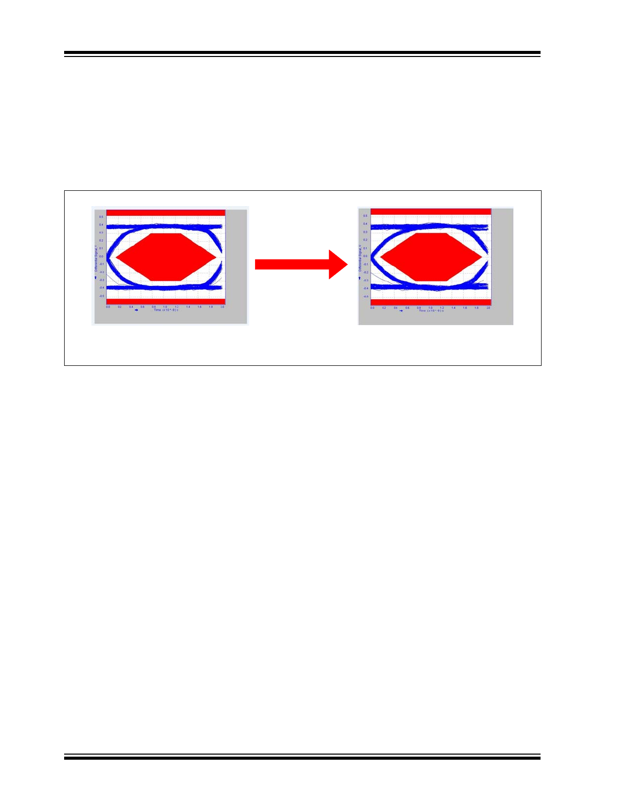
GENERAL DESCRIPTION
The USB3740B is a USB 2.0 compliant High Speed switch that provides robust ESD protection to the interface in an
extremely small package. Outstanding ESD robustness eliminates the need for external ESD protection devices to save
eBOM cost and PCB area.
The high bandwidth capabilities of the USB3740B enable extremely low high frequency loss and an exceptionally clean
USB 2.0 High Speed eye diagram.
1.1
Reference Document
Universal Serial Bus Specification, Revision 2.0
FIGURE 1-1:
USB3740B USB 2.0 HIGH SPEED EYE DIAGRAM
Input to Switch
Output of Switch
2011 - 2015 Microchip Technology Inc.
DS00001725D-page 5
USB3740B
2.0
PIN LAYOUT
2.1
Pin Diagram
The USB3740B is available in both a 0.4mm pitch QFN (1.3mm x 1.8mm x 0.55mm height) and 0.5mm pitch QFN
(1.6mm x 2.1mm x 0.55mm height) package. The 0.5mm pitch package can be ordered in standard or automotive con-
figurations. For additional ordering information, refer to the
Product Identification System
section.
2.2
Ball/Pin Definitions
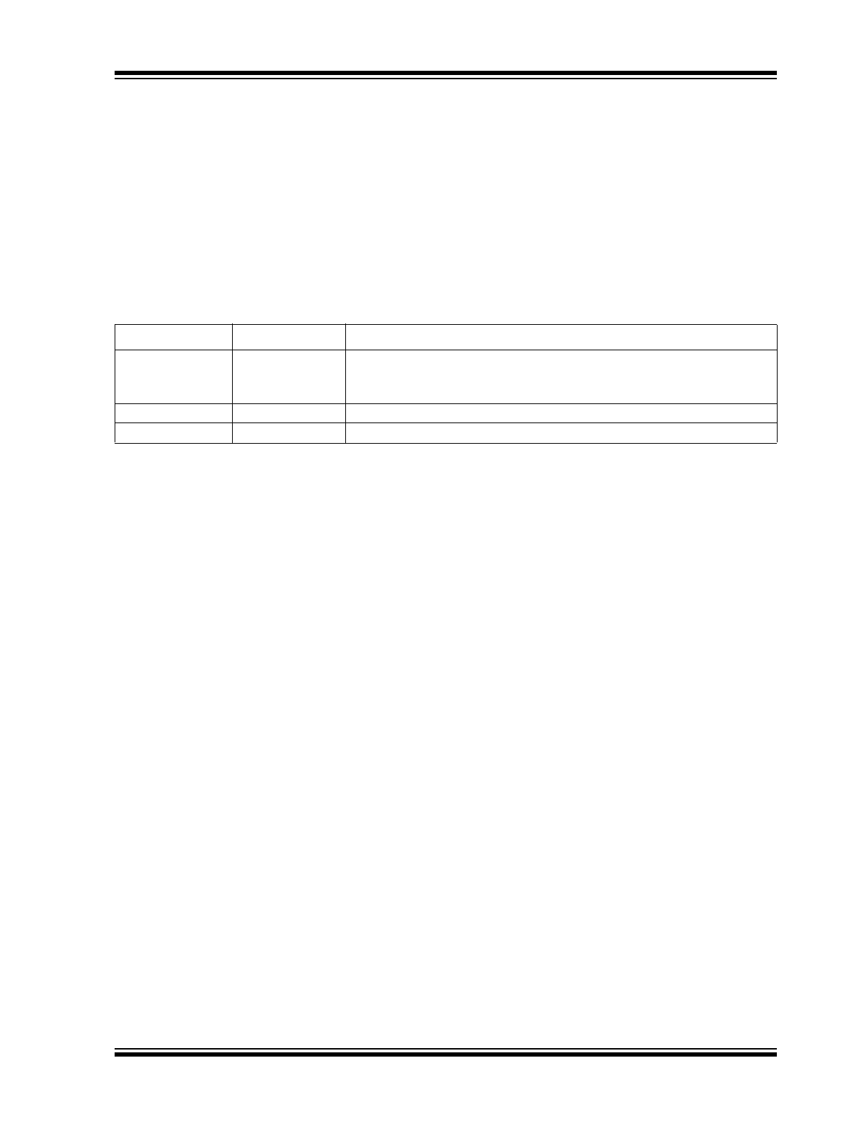
The following table details the ball/pin definitions for the package diagram above.
FIGURE 2-1:
USB3740B PACKAGE DIAGRAM
Pin
Name
Type/
Direction
Description
10
DP
Analog
USB Mux Output
9
DM
Analog
2
DP_1
Analog
USB Mux Input 1
1
DM_1
Analog
6
DP_2
Analog
USB Mux Input 2
7
DM_2
Analog
8
GND
Analog
Ground
5
VDD
Analog
Power
4
S
Digital Input
Switch control. Refer to
Table 4-1
.
3
OE_N
Digital Input
Active low switch Output Enable. Refer to
Table 4-1
.
DP
_
2
S
OE_N
DP
GND
VDD
DM
_
2
3
4
5
6
7
10
9
8
2
1
DM
DP
_
1
DM_
1
USB3740B
DS00001725D-page 6
2011 - 2015 Microchip Technology Inc.
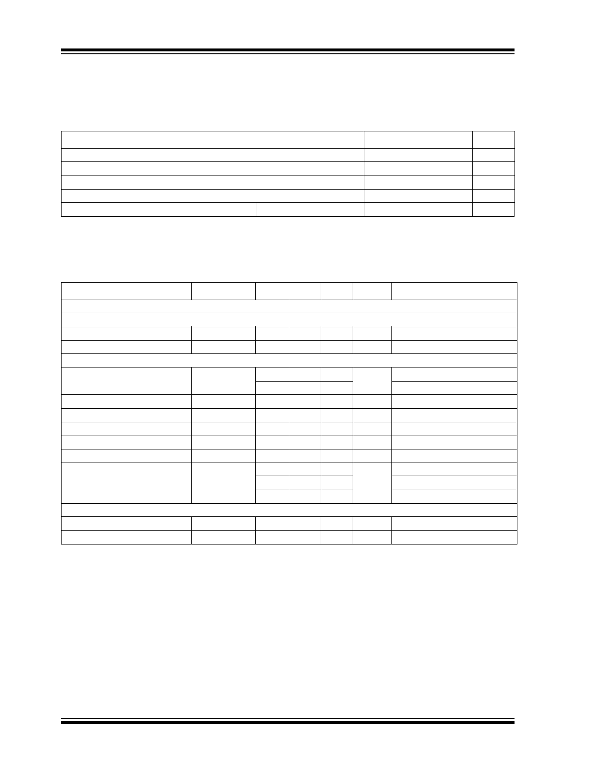
3.0
ELECTRICAL SPECIFICATIONS
3.1
Absolute Maximum Ratings
Stresses beyond the Absolute Maximum Ratings may damage the USB3740B.
3.2
Electrical Specifications
TABLE 3-1:
ABSOLUTE MAXIMUM RATINGS
Description
Rating
Unit
VDD Voltage to GND
-0.3 to 6.0
V
Any other pin to GND
-0.3 to VDD+0.5
V
Operating Temperature Range
-40 to +85
C
Storage Temperature Range
-55 to +150
C
ESD Rating
HBM
8,000
V
TABLE 3-2:
ELECTRICAL SPECIFICATIONS
Characteristic
Symbol
MIN
TYP
MAX
Units
Conditions
V
DD
= 5.0V, T
A
= -40C to 85C, all typical values at T
A
= 25C unless otherwise noted.
VDD Recommended Operating Conditions
Input Voltage
V
DD
3.0
5.5
V
Active/Standby
I
DD
30
175
nA
USB Mux Characteristics
USB Mux On Resistance
R
ON_USB
1
2
5
ohm
0V < Vin < 3.3V
1
2
2.5
0V < Vin < 0.4V
USB Mux Off Leakage
I
OFF_USB
100
200
nA
0V < Vin < 3.3V
On Capacitance
C
ON_USB
5
7
pF
V
DD
= 3V
Off Capacitance
C
OFF_USB
3
4
pF
V
DD
= 3V
Off Isolation
-30
-32
-40
dB
R
L
= 50 ohm, F = 250MHz
Crosstalk
-30
-45
-60
dB
R
L
= 50 ohm, F = 250MHz
Bandwidth (-3dB)
BW
950
1000
1100
MHz
R
L
= 50 ohm, C
L
= 0pF
850
950
980
R
L
= 50 ohm, C
L
= 5pF
530
560
600
R
L
= 50 ohm, C
L
= 10pF
Control Signal Characteristics
Input Logic High Threshold
V
IN_H
1.4
V
Input Logic Low Threshold
V
IN_L
0.4
V
2011 - 2015 Microchip Technology Inc.
DS00001725D-page 7
USB3740B
4.0
GENERAL OPERATION
The USB3740B is a high bandwidth switch suitable for many applications, including High Speed USB. The mux allows
high speed signals to pass through and still meet HS USB signaling requirements.
The USB3740B will protect the system from ESD stress events on all DP and DM pins. The USB3740B provides ESD
protection to the IEC-61000 ESD specification.
The USB mux is designed to pass High Speed USB signals to the USB connector, and allows for two USB inputs to be
multiplexed into one USB output.
The USB Mux is designed to pass USB signals from 0 to VDD. It is not designed to pass signals that go above VDD or
below ground.
The USB3740B switches are controlled by the digital signals OE_N and S, as shown in
Table 4-1
.
TABLE 4-1:
USB3740B SWITCH STATES DEFINITION
OE_N
S
Switch State
1
X
STANDBY:
• Both switch paths disconnected.
• Lowest power state
0
0
DP = DP1, DM = DM1:
0
1
DP = DP2, DM = DM2:

USB3740B
DS00001725D-page 8
2011 - 2015 Microchip Technology Inc.
5.0
APPLICATION NOTES
5.1
ESD Performance
The USB3740B is protected from ESD strikes. By eliminating the requirement for external ESD protection devices,
board space is conserved, and the board manufacturer is enabled to reduce cost. The advanced ESD structures inte-
grated into the USB3740B protect the device whether or not it is powered up.
5.1.1
HUMAN BODY MODEL (HBM) PERFORMANCE
HBM testing verifies the ability to withstand the ESD strikes like those that occur during handling and manufacturing,
and is done without power applied to the IC. To pass the test, the device must have no change in operation or perfor-
mance due to the event. The USB3740B HBM performance is detailed in
Table 3-1
.
2011 - 2015 Microchip Technology Inc.
DS00001725D-page 9
USB3740B
6.0
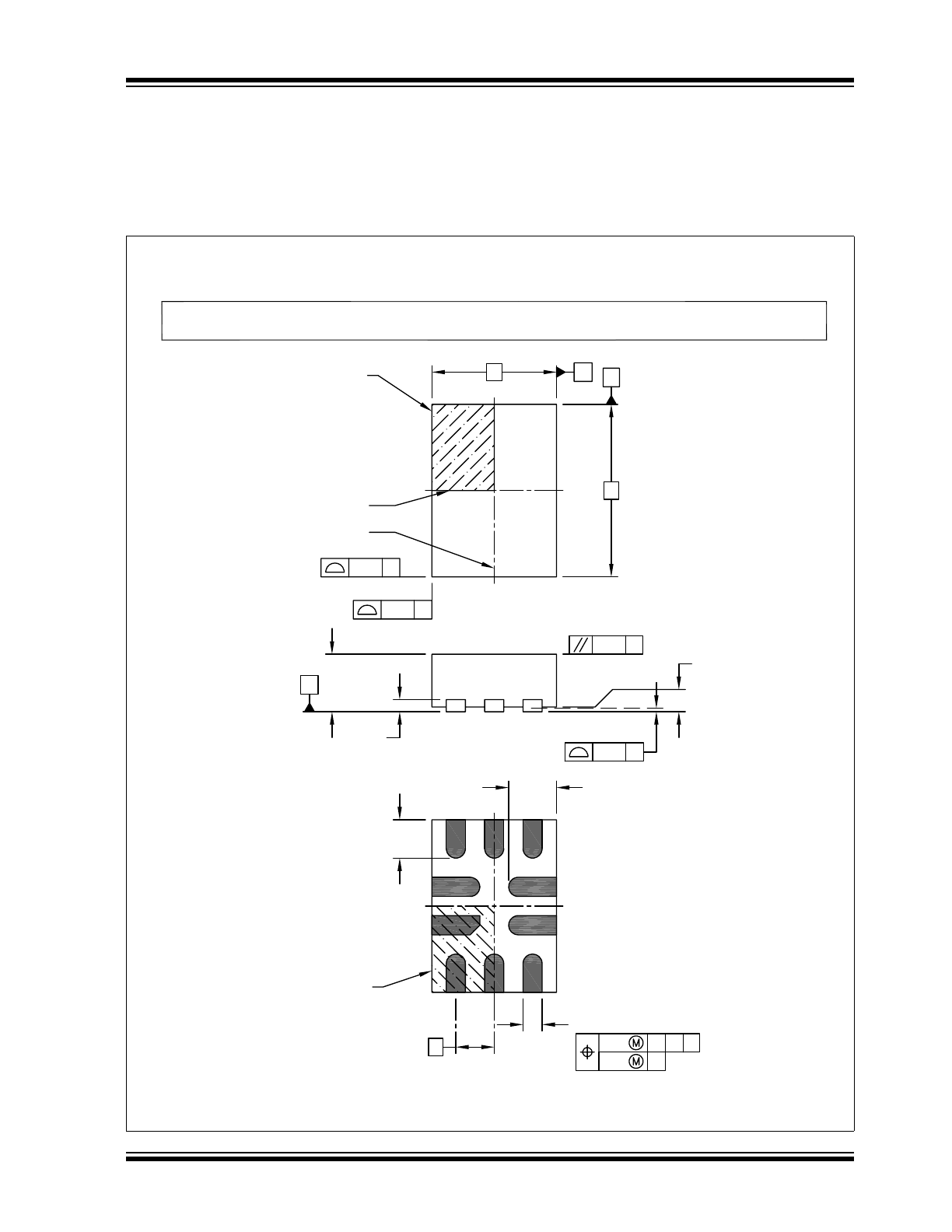
PACKAGE OUTLINES
6.1
1.3mm x 1.8mm QFN
FIGURE 6-1:
10-PIN, 1.3MM X 1.8MM QFN PACKAGE OUTLINE
B
A
0.10 C
0.10 C
0.07
C A B
0.05
C
(DATUM B)
(DATUM A)
C
SEATING
PLANE
NOTE 1
1
2
N
2X
TOP VIEW
SIDE VIEW
BOTTOM VIEW
NOTE 1
1
2
N
0.10 C
0.08 C
Microchip Technology Drawing C04-386A Sheet 1 of 2
2X
10X
For the most current package drawings, please see the Microchip Packaging Specification located at
http://www.microchip.com/packaging
Note:
10-Lead Ultra Thin Plastic Quad Flat, No Lead Package (2V) - 1.3x1.8x0.6 mm Body
[UQFN] Chip-On-Lead
D
E
e
6X L
10X b
A
(A3)
A1
4X L1
USB3740B
DS00001725D-page 10
2011 - 2015 Microchip Technology Inc.
FIGURE 6-2:
10-PIN, 1.3MM X 1.8MM QFN PACKAGE DIMENSIONS
Microchip Technology Drawing C04-386A Sheet 2 of 2
Number of Terminals
Overall Height
Terminal Width
Overall Width
Overall Length
Terminal Length
Terminal Thickness
Pitch
Standoff
Units
Dimension Limits
A1
A
b
D
A3
e
L
E
N
0.40 BSC
0.127 REF
0.35
0.15
0.50
0.00
0.20
1.30 BSC
0.40
0.55
0.02
1.80 BSC
MILLIMETERS
MIN
NOM
10
0.45
0.25
0.60
0.05
MAX
REF: Reference Dimension, usually without tolerance, for information purposes only.
BSC: Basic Dimension. Theoretically exact value shown without tolerances.
1.
2.
3.
Notes:
Pin 1 visual index feature may vary, but must be located within the hatched area.
Package is saw singulated
Dimensioning and tolerancing per ASME Y14.5M
For the most current package drawings, please see the Microchip Packaging Specification located at
http://www.microchip.com/packaging
Note:
Terminal Length
L1
0.45
0.50
0.55
10-Lead Ultra Thin Plastic Quad Flat, No Lead Package (2V) - 1.3x1.8x0.6 mm Body
[UQFN] Chip-On-Lead
2011 - 2015 Microchip Technology Inc.
DS00001725D-page 1
Features
• High Speed USB Mux for multiplexing the USB
lanes between different functions
- Switch the USB connector between two dif-
ferent functions
- Up to 1GHz Bandwidth
• USB Port ESD Protection (DP/DM)
- 8kV HBM
• flexPWR
TM
Technology
- 30nA Active/Standby Current
- Extremely low power design ideal for battery
powered applications
• Control inputs accommodate 1.8V to 5V inputs
• DP/DM tolerate up to 5.5V
• -40°C to +85°C Operating Temperature
• 10-pin, QFN, RoHS compliant package;
(1.3mm x 1.8mm x 0.55mm height, 0.4mm pitch)
• 10-pin, QFN, RoHS compliant package;
(1.6mm x 2.1mm x 0.55mm height, 0.5mm pitch)
• Automotive option
Block Diagram
OE_N
S
DP
DM
ES
D
Pr
ot
ec
ti
o
n
HS USB
Switch
DM_2
DP_2
U
S
B Conn
ecto
r
USB 2.0 PHY,
Processor, or
Accessory
Processor
GND
DM_1
DP_1
USB 2.0 PHY,
Processor, or
Accessory
DP
DM
DP
DM
DP
DM
USB3740B
VDD
VDD
ES
D
Pr
ot
ec
ti
o
n
USB3740B
High Speed USB 2.0 Switch with ESD Protection
and Low Standby Current
USB3740B
DS00001725D-page 2
2011 - 2015 Microchip Technology Inc.
TO OUR VALUED CUSTOMERS
It is our intention to provide our valued customers with the best documentation possible to ensure successful use of your Microchip
products. To this end, we will continue to improve our publications to better suit your needs. Our publications will be refined and
enhanced as new volumes and updates are introduced.
If you have any questions or comments regarding this publication, please contact the Marketing Communications Department via
E-mail at
docerrors@microchip.com
. We welcome your feedback.
Most Current Data Sheet
To obtain the most up-to-date version of this data sheet, please register at our Worldwide Web site at:
http://www.microchip.com
You can determine the version of a data sheet by examining its literature number found on the bottom outside corner of any page.
The last character of the literature number is the version number, (e.g., DS30000000A is version A of document DS30000000).
Errata
An errata sheet, describing minor operational differences from the data sheet and recommended workarounds, may exist for cur-
rent devices. As device/documentation issues become known to us, we will publish an errata sheet. The errata will specify the
revision of silicon and revision of document to which it applies.
To determine if an errata sheet exists for a particular device, please check with one of the following:
• Microchip’s Worldwide Web site;
http://www.microchip.com
• Your local Microchip sales office (see last page)
When contacting a sales office, please specify which device, revision of silicon and data sheet (include -literature number) you are
using.
Customer Notification System
Register on our web site at
www.microchip.com
to receive the most current information on all of our products.
2011 - 2015 Microchip Technology Inc.
DS00001725D-page 3
USB3740B
Table of Contents
1.0 General Description ........................................................................................................................................................................ 4
2.0 Pin Layout ....................................................................................................................................................................................... 5
3.0 Electrical Specifications .................................................................................................................................................................. 6
4.0 General Operation .......................................................................................................................................................................... 7
5.0 Application Notes ............................................................................................................................................................................ 8
6.0 Package Outlines ............................................................................................................................................................................ 9
The Microchip Web Site ...................................................................................................................................................................... 16
Customer Change Notification Service ............................................................................................................................................... 16
Customer Support ............................................................................................................................................................................... 16
Product Identification System ............................................................................................................................................................. 17
USB3740B
DS00001725D-page 4
2011 - 2015 Microchip Technology Inc.
1.0
GENERAL DESCRIPTION
The USB3740B is a USB 2.0 compliant High Speed switch that provides robust ESD protection to the interface in an
extremely small package. Outstanding ESD robustness eliminates the need for external ESD protection devices to save
eBOM cost and PCB area.
The high bandwidth capabilities of the USB3740B enable extremely low high frequency loss and an exceptionally clean
USB 2.0 High Speed eye diagram.
1.1
Reference Document
Universal Serial Bus Specification, Revision 2.0
FIGURE 1-1:
USB3740B USB 2.0 HIGH SPEED EYE DIAGRAM
Input to Switch
Output of Switch
2011 - 2015 Microchip Technology Inc.
DS00001725D-page 5
USB3740B
2.0
PIN LAYOUT
2.1
Pin Diagram
The USB3740B is available in both a 0.4mm pitch QFN (1.3mm x 1.8mm x 0.55mm height) and 0.5mm pitch QFN
(1.6mm x 2.1mm x 0.55mm height) package. The 0.5mm pitch package can be ordered in standard or automotive con-
figurations. For additional ordering information, refer to the
Product Identification System
section.
2.2
Ball/Pin Definitions
The following table details the ball/pin definitions for the package diagram above.
FIGURE 2-1:
USB3740B PACKAGE DIAGRAM
Pin
Name
Type/
Direction
Description
10
DP
Analog
USB Mux Output
9
DM
Analog
2
DP_1
Analog
USB Mux Input 1
1
DM_1
Analog
6
DP_2
Analog
USB Mux Input 2
7
DM_2
Analog
8
GND
Analog
Ground
5
VDD
Analog
Power
4
S
Digital Input
Switch control. Refer to
Table 4-1
.
3
OE_N
Digital Input
Active low switch Output Enable. Refer to
Table 4-1
.
DP
_
2
S
OE_N
DP
GND
VDD
DM
_
2
3
4
5
6
7
10
9
8
2
1
DM
DP
_
1
DM_
1
USB3740B
DS00001725D-page 6
2011 - 2015 Microchip Technology Inc.
3.0
ELECTRICAL SPECIFICATIONS
3.1
Absolute Maximum Ratings
Stresses beyond the Absolute Maximum Ratings may damage the USB3740B.
3.2
Electrical Specifications
TABLE 3-1:
ABSOLUTE MAXIMUM RATINGS
Description
Rating
Unit
VDD Voltage to GND
-0.3 to 6.0
V
Any other pin to GND
-0.3 to VDD+0.5
V
Operating Temperature Range
-40 to +85
C
Storage Temperature Range
-55 to +150
C
ESD Rating
HBM
8,000
V
TABLE 3-2:
ELECTRICAL SPECIFICATIONS
Characteristic
Symbol
MIN
TYP
MAX
Units
Conditions
V
DD
= 5.0V, T
A
= -40C to 85C, all typical values at T
A
= 25C unless otherwise noted.
VDD Recommended Operating Conditions
Input Voltage
V
DD
3.0
5.5
V
Active/Standby
I
DD
30
175
nA
USB Mux Characteristics
USB Mux On Resistance
R
ON_USB
1
2
5
ohm
0V < Vin < 3.3V
1
2
2.5
0V < Vin < 0.4V
USB Mux Off Leakage
I
OFF_USB
100
200
nA
0V < Vin < 3.3V
On Capacitance
C
ON_USB
5
7
pF
V
DD
= 3V
Off Capacitance
C
OFF_USB
3
4
pF
V
DD
= 3V
Off Isolation
-30
-32
-40
dB
R
L
= 50 ohm, F = 250MHz
Crosstalk
-30
-45
-60
dB
R
L
= 50 ohm, F = 250MHz
Bandwidth (-3dB)
BW
950
1000
1100
MHz
R
L
= 50 ohm, C
L
= 0pF
850
950
980
R
L
= 50 ohm, C
L
= 5pF
530
560
600
R
L
= 50 ohm, C
L
= 10pF
Control Signal Characteristics
Input Logic High Threshold
V
IN_H
1.4
V
Input Logic Low Threshold
V
IN_L
0.4
V
2011 - 2015 Microchip Technology Inc.
DS00001725D-page 7
USB3740B
4.0
GENERAL OPERATION
The USB3740B is a high bandwidth switch suitable for many applications, including High Speed USB. The mux allows
high speed signals to pass through and still meet HS USB signaling requirements.
The USB3740B will protect the system from ESD stress events on all DP and DM pins. The USB3740B provides ESD
protection to the IEC-61000 ESD specification.
The USB mux is designed to pass High Speed USB signals to the USB connector, and allows for two USB inputs to be
multiplexed into one USB output.
The USB Mux is designed to pass USB signals from 0 to VDD. It is not designed to pass signals that go above VDD or
below ground.
The USB3740B switches are controlled by the digital signals OE_N and S, as shown in
Table 4-1
.
TABLE 4-1:
USB3740B SWITCH STATES DEFINITION
OE_N
S
Switch State
1
X
STANDBY:
• Both switch paths disconnected.
• Lowest power state
0
0
DP = DP1, DM = DM1:
0
1
DP = DP2, DM = DM2:
USB3740B
DS00001725D-page 8
2011 - 2015 Microchip Technology Inc.
5.0
APPLICATION NOTES
5.1
ESD Performance
The USB3740B is protected from ESD strikes. By eliminating the requirement for external ESD protection devices,
board space is conserved, and the board manufacturer is enabled to reduce cost. The advanced ESD structures inte-
grated into the USB3740B protect the device whether or not it is powered up.
5.1.1
HUMAN BODY MODEL (HBM) PERFORMANCE
HBM testing verifies the ability to withstand the ESD strikes like those that occur during handling and manufacturing,
and is done without power applied to the IC. To pass the test, the device must have no change in operation or perfor-
mance due to the event. The USB3740B HBM performance is detailed in
Table 3-1
.
2011 - 2015 Microchip Technology Inc.
DS00001725D-page 9
USB3740B
6.0
PACKAGE OUTLINES
6.1
1.3mm x 1.8mm QFN
FIGURE 6-1:
10-PIN, 1.3MM X 1.8MM QFN PACKAGE OUTLINE
B
A
0.10 C
0.10 C
0.07
C A B
0.05
C
(DATUM B)
(DATUM A)
C
SEATING
PLANE
NOTE 1
1
2
N
2X
TOP VIEW
SIDE VIEW
BOTTOM VIEW
NOTE 1
1
2
N
0.10 C
0.08 C
Microchip Technology Drawing C04-386A Sheet 1 of 2
2X
10X
For the most current package drawings, please see the Microchip Packaging Specification located at
http://www.microchip.com/packaging
Note:
10-Lead Ultra Thin Plastic Quad Flat, No Lead Package (2V) - 1.3x1.8x0.6 mm Body
[UQFN] Chip-On-Lead
D
E
e
6X L
10X b
A
(A3)
A1
4X L1
USB3740B
DS00001725D-page 10
2011 - 2015 Microchip Technology Inc.
FIGURE 6-2:
10-PIN, 1.3MM X 1.8MM QFN PACKAGE DIMENSIONS
Microchip Technology Drawing C04-386A Sheet 2 of 2
Number of Terminals
Overall Height
Terminal Width
Overall Width
Overall Length
Terminal Length
Terminal Thickness
Pitch
Standoff
Units
Dimension Limits
A1
A
b
D
A3
e
L
E
N
0.40 BSC
0.127 REF
0.35
0.15
0.50
0.00
0.20
1.30 BSC
0.40
0.55
0.02
1.80 BSC
MILLIMETERS
MIN
NOM
10
0.45
0.25
0.60
0.05
MAX
REF: Reference Dimension, usually without tolerance, for information purposes only.
BSC: Basic Dimension. Theoretically exact value shown without tolerances.
1.
2.
3.
Notes:
Pin 1 visual index feature may vary, but must be located within the hatched area.
Package is saw singulated
Dimensioning and tolerancing per ASME Y14.5M
For the most current package drawings, please see the Microchip Packaging Specification located at
http://www.microchip.com/packaging
Note:
Terminal Length
L1
0.45
0.50
0.55
10-Lead Ultra Thin Plastic Quad Flat, No Lead Package (2V) - 1.3x1.8x0.6 mm Body
[UQFN] Chip-On-Lead