

2011-2015 Microchip Technology Inc.
DS00001584B-page 1
Features
• Integrated USB 2.0 Compatible 3-Port Hub.
• HSIC Upstream Port
• Advanced power saving features
- 1
μA Typical Standby Current
- Port goes into power saving state when no
devices are connected downstream
- Port is shutdown when port is disabled.
- Digital core shut down in Standby Mode
• Supports either Single-TT or Multi-TT configura-
tions for Full-Speed and Low-Speed connections.
• Enhanced configuration options available through
serial I
2
C Slave Port
- VID/PID/DID
- String Descriptors
- Configuration options for Hub.
• Internal Default configuration option when serial
I
2
C host not available.
• MultiTRAK
TM
- Dedicated Transaction Translator per port.
• PortMap
- Configurable port mapping and disable
sequencing.
• PortSwap
- Configurable differential intra-pair signal
swapping.
• PHYBoost
TM
- Programmable USB transceiver drive
strength for recovering signal integrity
• VariSense
TM
- Programmable USB receiver sensitivity
• flexPWR
®
Technology
- Low current design ideal for battery powered
applications
• Internal supply switching provides low power
modes
• External 12, 19.2, 24, 25, 26, 27, 38.4, or 52 MHz
clock input
• Internal 3.3V & 1.2V Voltage Regulators for single
supply operation.
- External VBAT and 1.8V dual supply input
option
• Internal Short Circuit protection of USB differential
signal pins.
• USB Port ESD Protection (DP/DM)
- ±15kV (air and contact discharge)
- IEC 61000-4-2 level 4 ESD protection without
external devices
• 25-pin WLCS (1.97mm x 1.97mm Wafer Level
Chip Scale) Package - 0.4mm ball pitch
• 32-pin SQFN (5.0 mm x 5.0 mm) Package
Applications
The USB3503 is targeted for applications where more
than one USB port is required. As mobile devices add
more features and the systems become more complex
it is necessary to have more than one USB port to take
communicate with the internal and peripheral devices.
• Mobile Phones
• Tablet Computers
• Ultra Mobile PCs
• Digital Still Cameras
• Digital Video Camcorders
• Gaming Consoles
• PDAs
• Portable Media Players
• GPS Personal Navigation Devices
• Media Players/Viewers
USB3503
USB 2.0 HSIC High-Speed Hub Controller Optimized
for Portable Applications

USB3503
DS00001584B-page 2
2011-2015 Microchip Technology Inc.
TO OUR VALUED CUSTOMERS
It is our intention to provide our valued customers with the best documentation possible to ensure successful use of your Microchip
products. To this end, we will continue to improve our publications to better suit your needs. Our publications will be refined and
enhanced as new volumes and updates are introduced.
If you have any questions or comments regarding this publication, please contact the Marketing Communications Department via
E-mail at
docerrors@microchip.com
. We welcome your feedback.
Most Current Data Sheet
To obtain the most up-to-date version of this data sheet, please register at our Worldwide Web site at:
http://www.microchip.com
You can determine the version of a data sheet by examining its literature number found on the bottom outside corner of any page.
The last character of the literature number is the version number, (e.g., DS30000000A is version A of document DS30000000).
Errata
An errata sheet, describing minor operational differences from the data sheet and recommended workarounds, may exist for cur-
rent devices. As device/documentation issues become known to us, we will publish an errata sheet. The errata will specify the
revision of silicon and revision of document to which it applies.
To determine if an errata sheet exists for a particular device, please check with one of the following:
• Microchip’s Worldwide Web site;
http://www.microchip.com
• Your local Microchip sales office (see last page)
When contacting a sales office, please specify which device, revision of silicon and data sheet (include -literature number) you are
using.
Customer Notification System
Register on our web site at
www.microchip.com
to receive the most current information on all of our products.

2011-2015 Microchip Technology Inc.
DS00001584B-page 3
USB3503
Table of Contents
1.0 General Description ........................................................................................................................................................................ 4
2.0 Acronyms and Definitions ............................................................................................................................................................... 6
3.0 USB3503 Pin Definitions ................................................................................................................................................................. 7
4.0 Modes of Operation ...................................................................................................................................................................... 15
5.0 Configuration Options ................................................................................................................................................................... 19
6.0 Serial Slave Interface .................................................................................................................................................................... 36
7.0 USB Descriptors ........................................................................................................................................................................... 39
8.0 Battery Charging ........................................................................................................................................................................... 48
9.0 Integrated Power Regulators ........................................................................................................................................................ 50
10.0 Specifications .............................................................................................................................................................................. 51
11.0 Application Reference ................................................................................................................................................................. 58
12.0 Package Outlines, Tape & Reel Drawings, Package Marking .................................................................................................... 61
Appendix A: Data sheet Revision History ........................................................................................................................................... 69
The Microchip Web Site ...................................................................................................................................................................... 70
Customer Change Notification Service ............................................................................................................................................... 70
Customer Support ............................................................................................................................................................................... 70
USB3503 25-WLCSP Product Identification System .......................................................................................................................... 71
USB3503 32-SQFN Product Identification System ............................................................................................................................. 71
USB3503
DS00001584B-page 4
2011-2015 Microchip Technology Inc.
1.0
GENERAL DESCRIPTION
The USB3503 is a low-power, USB 2.0 hub controller with HSIC upstream connectivity and three USB 2.0 downtream
ports. The USB3503 operates as a hi-speed hub and supports low-speed, full-speed, and hi-speed downstream devices
on all of the enabled downstream ports.
The USB3503 has been specifically optimized for mobile embedded applications. The pin-count has been reduced by
optimizing the USB3503 for mobile battery-powered embedded systems where power consumption, small package
size, and minimal BOM are critical design requirements. Standby mode power has been minimized. Instead of a dedi-
cated crystal, reference clock inputs are aligned to mobile applications. Flexible integrated power regulators ease inte-
gration into battery powered devices. All required resistors on the USB ports are integrated into the hub. This includes
all series termination resistors on D+ and D– pins and all required pull-down resistors on D+ and D– pins.
The USB3503 includes programmable features such as:
MultiTRAK
TM
Technology, which utilizes a dedicated Transaction Translator (TT) per port to maintain consistent full-
speed data throughput regardless of the number of active downstream connections. MultiTRAK
TM
outperforms conven-
tional USB 2.0 hubs with a single TT in USB full-speed data transfers.
PortMap, which provides flexible port mapping and disable sequences. The downstream ports of a USB3503 hub can
be reordered or disabled in any sequence to support multiple platform designs with minimum effort. For any port that is
disabled, the USB3503 hub controllers automatically reorder the remaining ports to match the USB host controller’s port
numbering scheme.
PortSwap, which adds per-port programmability to USB differential-pair pin locations. PortSwap allows direct alignment
of USB signals (D+/D-) to connectors to avoid uneven trace length or crossing of the USB differential signals on the
PCB.
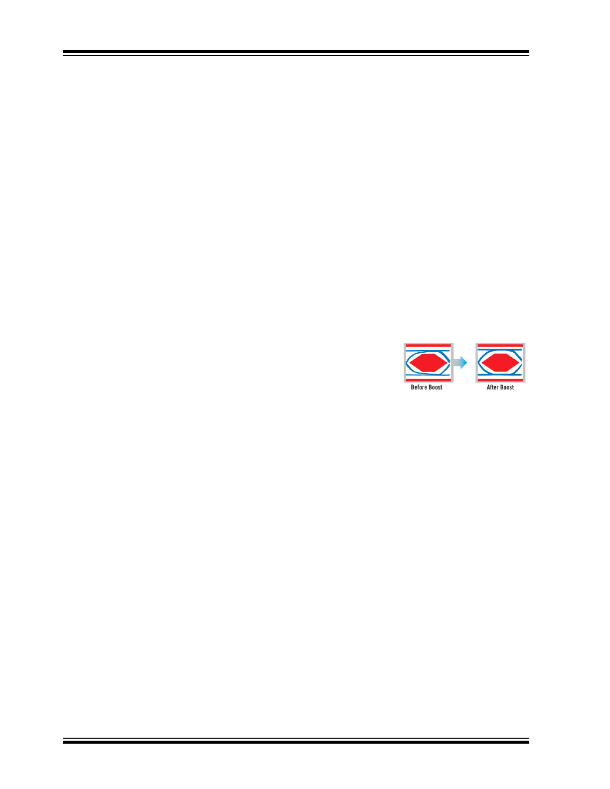
PHYBoost, which provides programmable levels of Hi-Speed USB signal drive
strength in the downstream port transceivers. PHYBoost attempts to restore USB sig-
nal integrity in a compromised system environment. The graphic on the right shows
an example of Hi-Speed USB eye diagrams before and after PHYBoost signal integ-
rity restoration.
VariSense, which controls the USB receiver sensitivity enabling programmable lev-
els of USB signal receive sensitivity. This capability allows operation in a sub-optimal
system environment, such as when a captive USB cable is used.
1.1
Customer Selectable Features
A default configuration is available in the USB3503 following a reset. This configuration may be sufficient for most appli-
cations. The USB3503 hub may also be configured by an external microcontroller. When using the microcontroller inter-
face, the hub appears as an I
2
C slave device.
The USB3503 hub supports customer selectable features including:
• Optional customer configuration via I
2
C.
• Supports compound devices on a port-by-port basis.
• Customizable vendor ID, product ID, and device ID.
• Configurable downstream port power-on time reported to the host.
• Supports indication of the maximum current that the hub consumes from the USB upstream port.
• Supports Indication of the maximum current required for the hub controller.
• Configurable as a either a Self-Powered or Bus-Powered Hub
• Supports custom string descriptors (up to 30 characters):
- Product string
- Manufacturer string
- Serial number string
• When available, I
2
C configurable options for default configuration may include:
- Downstream ports as non-removable ports
- Downstream ports as disabled ports
- USB signal drive strength
- USB receiver sensitivity
- USB differential pair pin location
2011-2015 Microchip Technology Inc.
DS00001584B-page 5
USB3503
1.1.1
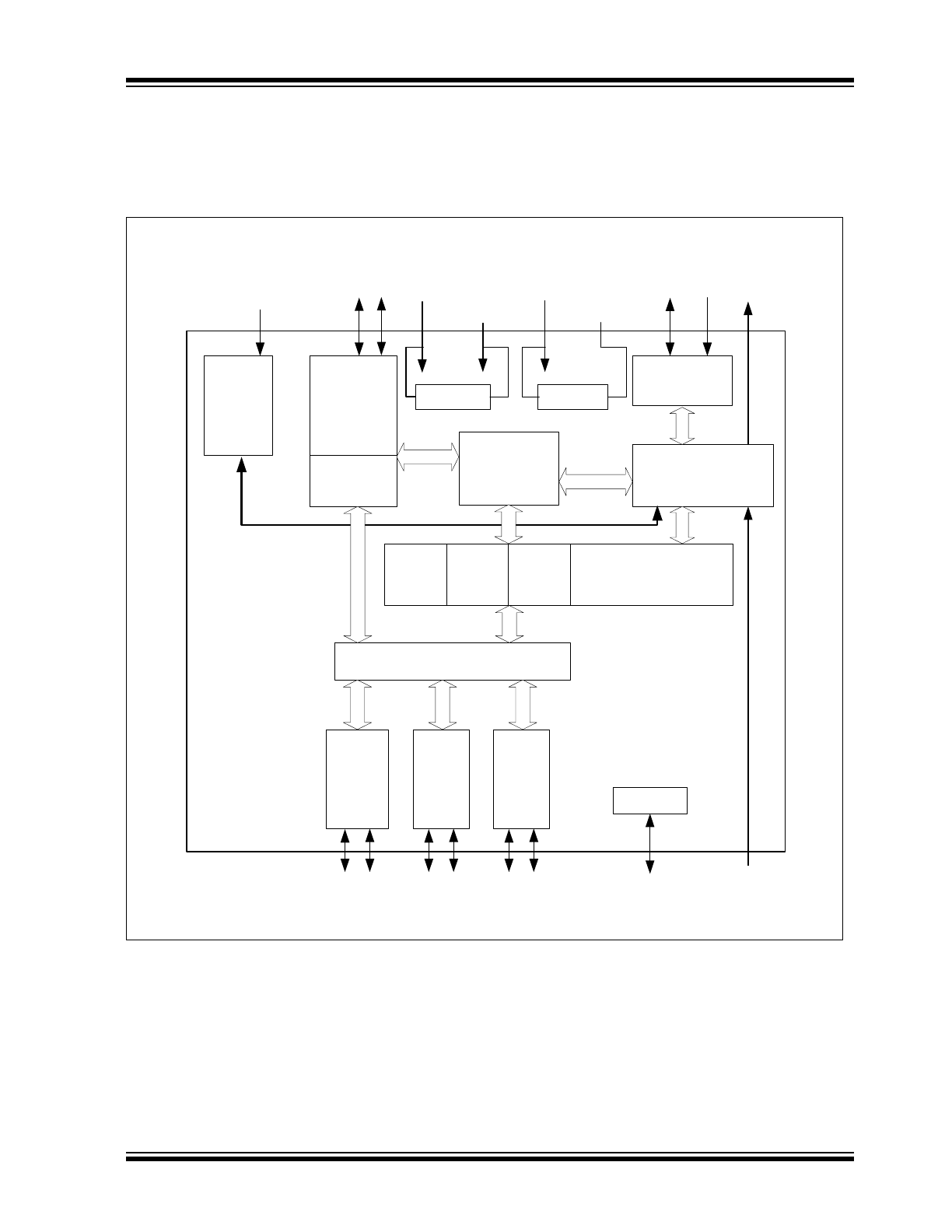
BLOCK DIAGRAM
FIGURE 1-1:
USB3503 BLOCK DIAGRAM
Upstream
HSIC
Upstream HSIC
Port
Repeater
Controller
SIE
Serial
Interface
PLL
REF_CLK
To I2C Master
Routing & Port Re-Ordering Logic
SCL
SDA
Port Controller
PHY#3
USB Data
Downstream
Mode
Control
-
Standby
Hub Mode
TT #3
TT #2
TT #1
PHY#2
PHY#1
USB Data
Downstream
USB Data
Downstream
1.2V Reg
RESET_N
3.3V Reg
INT_N
HUB_CONNECT
VDD33_BYP
VDD12_BYP
VBAT
VDD_CORE_REG

USB3503
DS00001584B-page 6
2011-2015 Microchip Technology Inc.
2.0
ACRONYMS AND DEFINITIONS
2.1
Acronyms
EP: Endpoint
FS: Full-Speed
HS: Hi-Speed
I
2
C
®
: Inter-Integrated
Circuit
1
LS: Low-Speed
HSIC: High-Speed
Inter-Chip
2.2
Reference Documents
1.
USB Engineering Change Notice dated December 29th, 2004, UNICODE UTF-16LE For String Descriptors.
2.
Universal Serial Bus Specification, Revision 2.0, Dated April 27th, 2000.
3.
Battery Charging Specification, Revision 1.1, Release Candidate 10, Dated Sept. 22, 2008
4.
High-Speed Inter-Chip USB Electrical Specification, Version 1.0, Dated Sept. 23, 2007
1. I
2
C is a registered trademark of Philips Corporation.
2011-2015 Microchip Technology Inc.
DS00001584B-page 7
USB3503
3.0
USB3503 PIN DEFINITIONS
3.1
Pin Configuration
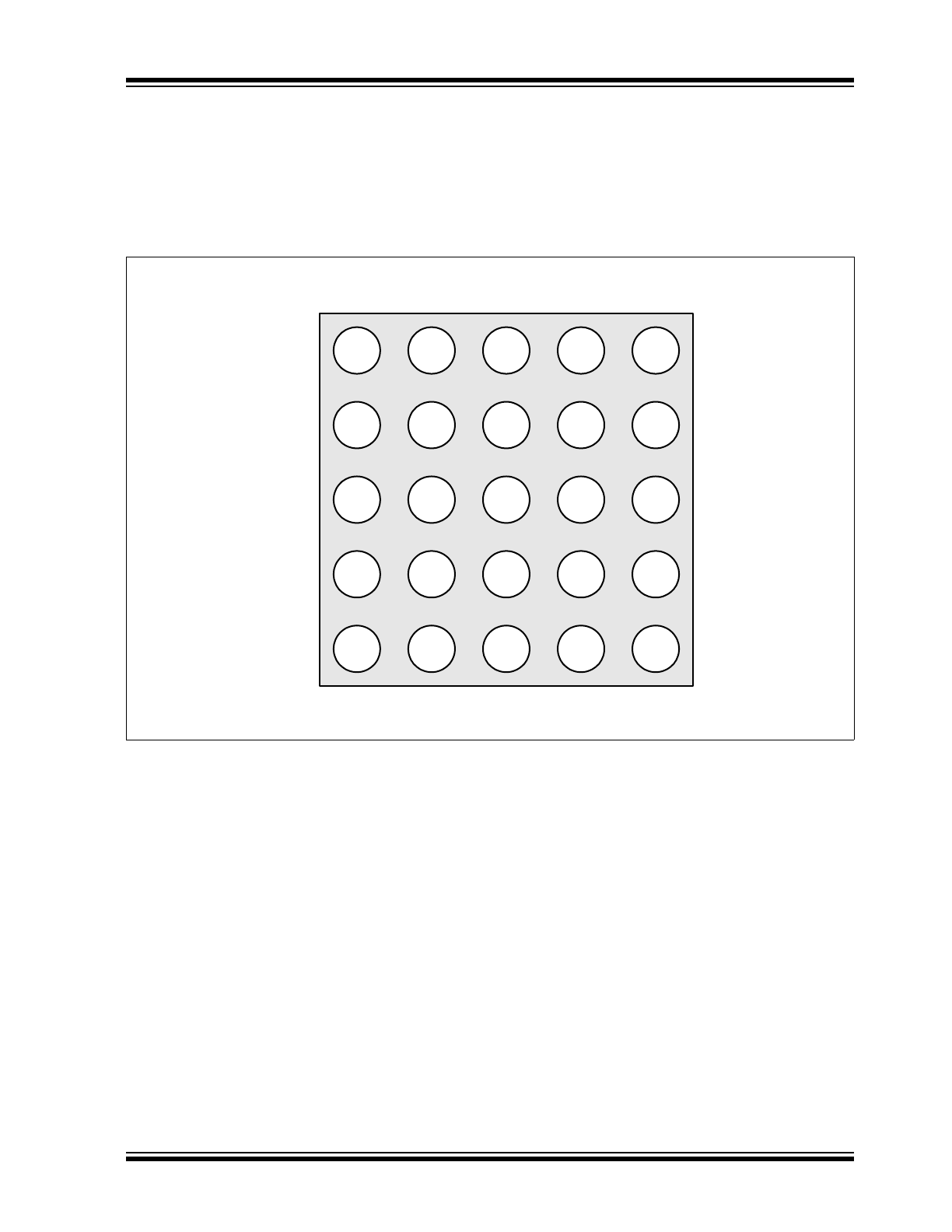
Figure 3-1
details the 25-ball WLCSP package.
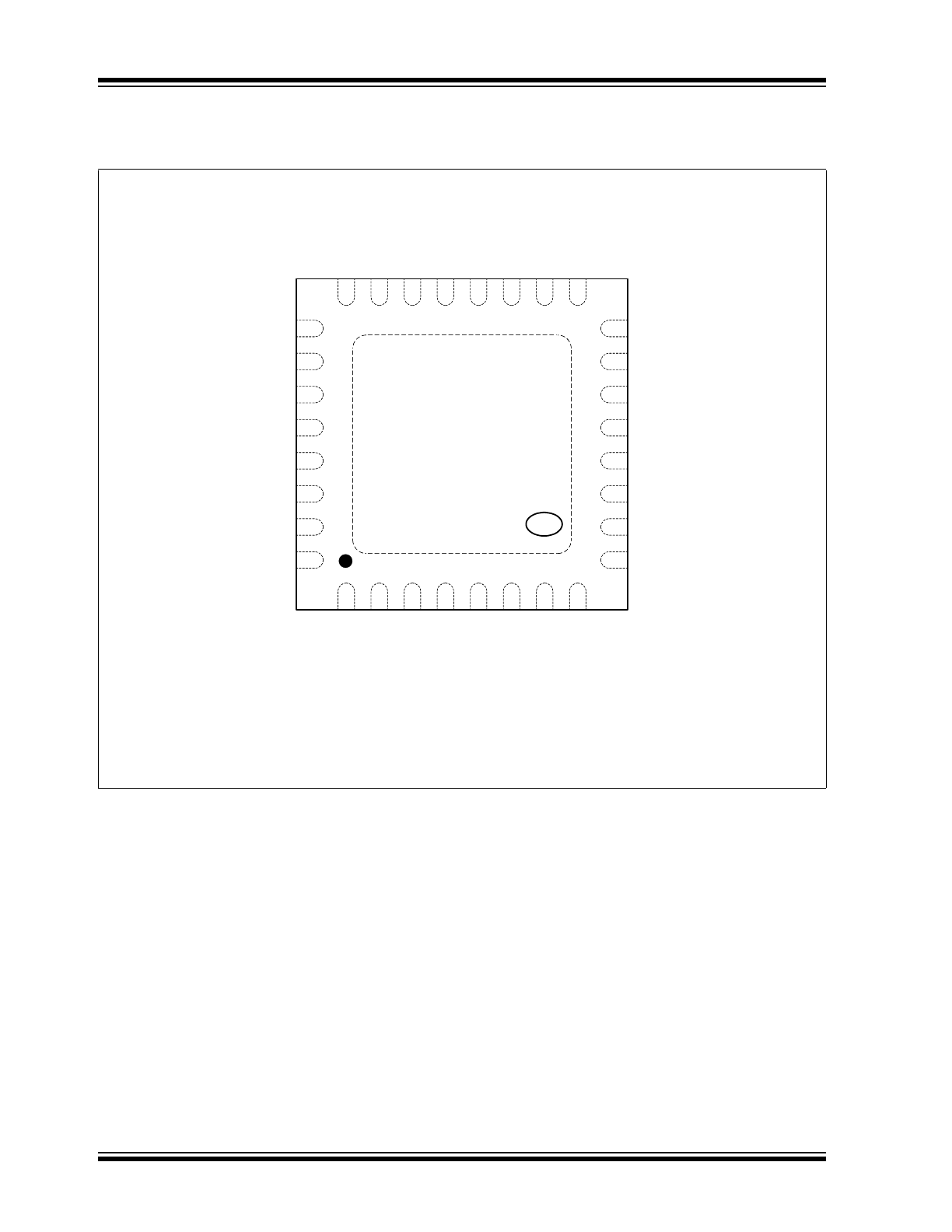
Figure 3-2
details the 32-pin SQFN package pin configuration. Signal
definitions are provided in
Section 3.2
.
FIGURE 3-1:
USB3503 25-BALL WLCSP PACKAGE
A
E
D
C
B
1
5
4
3
2
TOP VIEW
USB3503
DS00001584B-page 8
2011-2015 Microchip Technology Inc.
FIGURE 3-2:
USB3503 32-PIN SQFN PACKAGE
Note: Exposed pad (VSS) on bottom of package must be connected to ground.
STROBE
1
2
3
4
5
6
7
8
9
10
11
12
13
14
15
16
24
23
22
21
20
19
18
17
32
31
30
29
28
27
26
25
SC
L
SDA
VDD12_BY
P
IN
T_
N
PRTPW
R
NC
H
U
B
_C
O
N
NE
CT
O
C
S_N
U
SB
DN1
_DP
USB
DN1_DM
USB
DN2_DP
USB
DN2_DM
USB
DN3_DP
USB
DN3_DM
NC
NC
VBAT
VDD33_BYP
NC
VDD_CORE_REG
REFCLK
RBIAS
NC
VDD33_BYP
DATA
NC
VDD12_BYP
RESET_N
VDD12_BYP
REF_SEL0
REF_SEL1
USB3503
3
e

2011-2015 Microchip Technology Inc.
DS00001584B-page 9
USB3503
3.2
Signal Definitions
WLCSP
Ball
SQFN
Pin
Name
Description
E2
15
DATA
Upstream HSIC DATA pin of the USB Interface
E1
16
STROBE
Upstream HSIC STROBE pin of the USB Interface
A5
32
VDD33_BYP
3.3 V Regulator Bypass
C4
4
PRTPWR
Port Power Control Output
B4
1
OCS_N
Over Current Sense Input
A1
24
USBDN1_DP
USB downstream Port 1 D+ data pin
B1
23
USBDN1_DM
USB downstream Port 1 D- data pin
C2
22
USBDN2_DP
USB downstream Port 2 D+ data pin
D2
21
USBDN2_DM
USB downstream Port 2 D- data pin
C1
20
USBDN3_DP
USB downstream Port 3 D+ data pin
D1
19
USBDN3_DM
USB downstream Port 3 D- data pin
E5
8
SCL I
2
C clock input
D5
7
SDA I
2
C bi-directional data pin
E3
12
RESET_N
Active low reset signal
B5
2
HUB_CONNECT
Hub Connect
C5
5
INT_N
Active low interrupt signal
D4
9
REF_SEL1
Reference Clock Select 1 input
E4
10
REF_SEL0
Reference Clock Select 0 input
B3
29
REFCLK Reference
Clock
input
A4
30
RBIAS
Bias Resistor pin
D3
6,11,13
VDD12_BYP
1.2 V Regulator
A2
26
VDD33_BYP
3.3 V Regulator
B2
25
VBAT
Voltage input from the battery supply
A3
28
VDD_CORE_REG
Power supply input to 1.2V regulator for digital logic core
C3
e-pad
VSS Ground
-
3,14,17,
18,27,31
NC
No connect

USB3503
DS00001584B-page 10
2011-2015 Microchip Technology Inc.
3.3
Pin Descriptions
This section provides a detailed description of each signal. The signals are arranged in functional groups according to
their associated interface.
The terms assertion and negation are used. This is done to avoid confusion when working with a mixture of “active low”
and “active high” signal. The term “assert”, or “assertion” indicates that a signal is active, independent of whether that
level is represented by a high or low voltage. The term “negate”, or “negation” indicates that a signal is inactive.
3.3.1
PIN DEFINITION
TABLE 3-1:
PIN DESCRIPTIONS
Name
Symbol
Type
Description
UPSTREAM HIGH SPEED INTER-CHIP INTERFACE
HSIC Clock/Strobe
STROBE
I/O
HSIC Upstream Hub Strobe pin
HSIC Data
DATA
I/O
HSIC Upstream Hub Data pin
High-Speed USB Data
&
Port Disable Strap Option
USBDN_DP[2:1]
&
USBDN_DM[2:1]
A-I/O
These pins connect to the downstream USB
peripheral devices attached to the hub’s ports
Downstream Port Disable Strap option:
This pin will be sampled at RESET_N negation to
determine if the port is disabled.
Both USB data pins for the corresponding port
must be tied to VDD33_BYP to disable the
associated downstream port.
HS USB Data
USBDN_DP[3]
&
USBDN_DM[3]
A-I/O
These pins connect to the downstream USB
peripheral devices attached to the hub’s ports.
There is no downstream Port Disable Strap
option on these ports.
SERIAL PORT INTERFACE
Serial Data
SDA
I/OD
I
2
C Serial Data
Serial Clock
SCL
I
Serial Clock (SCL)
Interrupt
INT_N
OD
Interrupt
The function of this pin is determined by the
setting in the CFGP.INTSUSP configuration
register.
When CFGP.INTSUSP = 0 (General Interrupt)
A transition from high to low identifies when one of
the interrupt enabled status registers has been
updated.
SOC must update the Serial Port Interrupt Status
Register to reset the interrupt pin high.
When CFGP.INTSUSP = 1 (Suspend Interrupt)
Indicates USB state of the hub.
‘Asserted’ low = Unconfigured or configured and in
USB Suspend
‘Negated’ high = Hub is configured, and is active
(i.e., not in suspend)
If unused, this pin must be tied to VDD33_BYP.
2011-2015 Microchip Technology Inc.
DS00001584B-page 1
Features
• Integrated USB 2.0 Compatible 3-Port Hub.
• HSIC Upstream Port
• Advanced power saving features
- 1
μA Typical Standby Current
- Port goes into power saving state when no
devices are connected downstream
- Port is shutdown when port is disabled.
- Digital core shut down in Standby Mode
• Supports either Single-TT or Multi-TT configura-
tions for Full-Speed and Low-Speed connections.
• Enhanced configuration options available through
serial I
2
C Slave Port
- VID/PID/DID
- String Descriptors
- Configuration options for Hub.
• Internal Default configuration option when serial
I
2
C host not available.
• MultiTRAK
TM
- Dedicated Transaction Translator per port.
• PortMap
- Configurable port mapping and disable
sequencing.
• PortSwap
- Configurable differential intra-pair signal
swapping.
• PHYBoost
TM
- Programmable USB transceiver drive
strength for recovering signal integrity
• VariSense
TM
- Programmable USB receiver sensitivity
• flexPWR
®
Technology
- Low current design ideal for battery powered
applications
• Internal supply switching provides low power
modes
• External 12, 19.2, 24, 25, 26, 27, 38.4, or 52 MHz
clock input
• Internal 3.3V & 1.2V Voltage Regulators for single
supply operation.
- External VBAT and 1.8V dual supply input
option
• Internal Short Circuit protection of USB differential
signal pins.
• USB Port ESD Protection (DP/DM)
- ±15kV (air and contact discharge)
- IEC 61000-4-2 level 4 ESD protection without
external devices
• 25-pin WLCS (1.97mm x 1.97mm Wafer Level
Chip Scale) Package - 0.4mm ball pitch
• 32-pin SQFN (5.0 mm x 5.0 mm) Package
Applications
The USB3503 is targeted for applications where more
than one USB port is required. As mobile devices add
more features and the systems become more complex
it is necessary to have more than one USB port to take
communicate with the internal and peripheral devices.
• Mobile Phones
• Tablet Computers
• Ultra Mobile PCs
• Digital Still Cameras
• Digital Video Camcorders
• Gaming Consoles
• PDAs
• Portable Media Players
• GPS Personal Navigation Devices
• Media Players/Viewers
USB3503
USB 2.0 HSIC High-Speed Hub Controller Optimized
for Portable Applications
USB3503
DS00001584B-page 2
2011-2015 Microchip Technology Inc.
TO OUR VALUED CUSTOMERS
It is our intention to provide our valued customers with the best documentation possible to ensure successful use of your Microchip
products. To this end, we will continue to improve our publications to better suit your needs. Our publications will be refined and
enhanced as new volumes and updates are introduced.
If you have any questions or comments regarding this publication, please contact the Marketing Communications Department via
E-mail at
docerrors@microchip.com
. We welcome your feedback.
Most Current Data Sheet
To obtain the most up-to-date version of this data sheet, please register at our Worldwide Web site at:
http://www.microchip.com
You can determine the version of a data sheet by examining its literature number found on the bottom outside corner of any page.
The last character of the literature number is the version number, (e.g., DS30000000A is version A of document DS30000000).
Errata
An errata sheet, describing minor operational differences from the data sheet and recommended workarounds, may exist for cur-
rent devices. As device/documentation issues become known to us, we will publish an errata sheet. The errata will specify the
revision of silicon and revision of document to which it applies.
To determine if an errata sheet exists for a particular device, please check with one of the following:
• Microchip’s Worldwide Web site;
http://www.microchip.com
• Your local Microchip sales office (see last page)
When contacting a sales office, please specify which device, revision of silicon and data sheet (include -literature number) you are
using.
Customer Notification System
Register on our web site at
www.microchip.com
to receive the most current information on all of our products.
2011-2015 Microchip Technology Inc.
DS00001584B-page 3
USB3503
Table of Contents
1.0 General Description ........................................................................................................................................................................ 4
2.0 Acronyms and Definitions ............................................................................................................................................................... 6
3.0 USB3503 Pin Definitions ................................................................................................................................................................. 7
4.0 Modes of Operation ...................................................................................................................................................................... 15
5.0 Configuration Options ................................................................................................................................................................... 19
6.0 Serial Slave Interface .................................................................................................................................................................... 36
7.0 USB Descriptors ........................................................................................................................................................................... 39
8.0 Battery Charging ........................................................................................................................................................................... 48
9.0 Integrated Power Regulators ........................................................................................................................................................ 50
10.0 Specifications .............................................................................................................................................................................. 51
11.0 Application Reference ................................................................................................................................................................. 58
12.0 Package Outlines, Tape & Reel Drawings, Package Marking .................................................................................................... 61
Appendix A: Data sheet Revision History ........................................................................................................................................... 69
The Microchip Web Site ...................................................................................................................................................................... 70
Customer Change Notification Service ............................................................................................................................................... 70
Customer Support ............................................................................................................................................................................... 70
USB3503 25-WLCSP Product Identification System .......................................................................................................................... 71
USB3503 32-SQFN Product Identification System ............................................................................................................................. 71
USB3503
DS00001584B-page 4
2011-2015 Microchip Technology Inc.
1.0
GENERAL DESCRIPTION
The USB3503 is a low-power, USB 2.0 hub controller with HSIC upstream connectivity and three USB 2.0 downtream
ports. The USB3503 operates as a hi-speed hub and supports low-speed, full-speed, and hi-speed downstream devices
on all of the enabled downstream ports.
The USB3503 has been specifically optimized for mobile embedded applications. The pin-count has been reduced by
optimizing the USB3503 for mobile battery-powered embedded systems where power consumption, small package
size, and minimal BOM are critical design requirements. Standby mode power has been minimized. Instead of a dedi-
cated crystal, reference clock inputs are aligned to mobile applications. Flexible integrated power regulators ease inte-
gration into battery powered devices. All required resistors on the USB ports are integrated into the hub. This includes
all series termination resistors on D+ and D– pins and all required pull-down resistors on D+ and D– pins.
The USB3503 includes programmable features such as:
MultiTRAK
TM
Technology, which utilizes a dedicated Transaction Translator (TT) per port to maintain consistent full-
speed data throughput regardless of the number of active downstream connections. MultiTRAK
TM
outperforms conven-
tional USB 2.0 hubs with a single TT in USB full-speed data transfers.
PortMap, which provides flexible port mapping and disable sequences. The downstream ports of a USB3503 hub can
be reordered or disabled in any sequence to support multiple platform designs with minimum effort. For any port that is
disabled, the USB3503 hub controllers automatically reorder the remaining ports to match the USB host controller’s port
numbering scheme.
PortSwap, which adds per-port programmability to USB differential-pair pin locations. PortSwap allows direct alignment
of USB signals (D+/D-) to connectors to avoid uneven trace length or crossing of the USB differential signals on the
PCB.
PHYBoost, which provides programmable levels of Hi-Speed USB signal drive
strength in the downstream port transceivers. PHYBoost attempts to restore USB sig-
nal integrity in a compromised system environment. The graphic on the right shows
an example of Hi-Speed USB eye diagrams before and after PHYBoost signal integ-
rity restoration.
VariSense, which controls the USB receiver sensitivity enabling programmable lev-
els of USB signal receive sensitivity. This capability allows operation in a sub-optimal
system environment, such as when a captive USB cable is used.
1.1
Customer Selectable Features
A default configuration is available in the USB3503 following a reset. This configuration may be sufficient for most appli-
cations. The USB3503 hub may also be configured by an external microcontroller. When using the microcontroller inter-
face, the hub appears as an I
2
C slave device.
The USB3503 hub supports customer selectable features including:
• Optional customer configuration via I
2
C.
• Supports compound devices on a port-by-port basis.
• Customizable vendor ID, product ID, and device ID.
• Configurable downstream port power-on time reported to the host.
• Supports indication of the maximum current that the hub consumes from the USB upstream port.
• Supports Indication of the maximum current required for the hub controller.
• Configurable as a either a Self-Powered or Bus-Powered Hub
• Supports custom string descriptors (up to 30 characters):
- Product string
- Manufacturer string
- Serial number string
• When available, I
2
C configurable options for default configuration may include:
- Downstream ports as non-removable ports
- Downstream ports as disabled ports
- USB signal drive strength
- USB receiver sensitivity
- USB differential pair pin location
2011-2015 Microchip Technology Inc.
DS00001584B-page 5
USB3503
1.1.1
BLOCK DIAGRAM
FIGURE 1-1:
USB3503 BLOCK DIAGRAM
Upstream
HSIC
Upstream HSIC
Port
Repeater
Controller
SIE
Serial
Interface
PLL
REF_CLK
To I2C Master
Routing & Port Re-Ordering Logic
SCL
SDA
Port Controller
PHY#3
USB Data
Downstream
Mode
Control
-
Standby
Hub Mode
TT #3
TT #2
TT #1
PHY#2
PHY#1
USB Data
Downstream
USB Data
Downstream
1.2V Reg
RESET_N
3.3V Reg
INT_N
HUB_CONNECT
VDD33_BYP
VDD12_BYP
VBAT
VDD_CORE_REG
USB3503
DS00001584B-page 6
2011-2015 Microchip Technology Inc.
2.0
ACRONYMS AND DEFINITIONS
2.1
Acronyms
EP: Endpoint
FS: Full-Speed
HS: Hi-Speed
I
2
C
®
: Inter-Integrated
Circuit
1
LS: Low-Speed
HSIC: High-Speed
Inter-Chip
2.2
Reference Documents
1.
USB Engineering Change Notice dated December 29th, 2004, UNICODE UTF-16LE For String Descriptors.
2.
Universal Serial Bus Specification, Revision 2.0, Dated April 27th, 2000.
3.
Battery Charging Specification, Revision 1.1, Release Candidate 10, Dated Sept. 22, 2008
4.
High-Speed Inter-Chip USB Electrical Specification, Version 1.0, Dated Sept. 23, 2007
1. I
2
C is a registered trademark of Philips Corporation.
2011-2015 Microchip Technology Inc.
DS00001584B-page 7
USB3503
3.0
USB3503 PIN DEFINITIONS
3.1
Pin Configuration
Figure 3-1
details the 25-ball WLCSP package.
Figure 3-2
details the 32-pin SQFN package pin configuration. Signal
definitions are provided in
Section 3.2
.
FIGURE 3-1:
USB3503 25-BALL WLCSP PACKAGE
A
E
D
C
B
1
5
4
3
2
TOP VIEW
USB3503
DS00001584B-page 8
2011-2015 Microchip Technology Inc.
FIGURE 3-2:
USB3503 32-PIN SQFN PACKAGE
Note: Exposed pad (VSS) on bottom of package must be connected to ground.
STROBE
1
2
3
4
5
6
7
8
9
10
11
12
13
14
15
16
24
23
22
21
20
19
18
17
32
31
30
29
28
27
26
25
SC
L
SDA
VDD12_BY
P
IN
T_
N
PRTPW
R
NC
H
U
B
_C
O
N
NE
CT
O
C
S_N
U
SB
DN1
_DP
USB
DN1_DM
USB
DN2_DP
USB
DN2_DM
USB
DN3_DP
USB
DN3_DM
NC
NC
VBAT
VDD33_BYP
NC
VDD_CORE_REG
REFCLK
RBIAS
NC
VDD33_BYP
DATA
NC
VDD12_BYP
RESET_N
VDD12_BYP
REF_SEL0
REF_SEL1
USB3503
3
e
2011-2015 Microchip Technology Inc.
DS00001584B-page 9
USB3503
3.2
Signal Definitions
WLCSP
Ball
SQFN
Pin
Name
Description
E2
15
DATA
Upstream HSIC DATA pin of the USB Interface
E1
16
STROBE
Upstream HSIC STROBE pin of the USB Interface
A5
32
VDD33_BYP
3.3 V Regulator Bypass
C4
4
PRTPWR
Port Power Control Output
B4
1
OCS_N
Over Current Sense Input
A1
24
USBDN1_DP
USB downstream Port 1 D+ data pin
B1
23
USBDN1_DM
USB downstream Port 1 D- data pin
C2
22
USBDN2_DP
USB downstream Port 2 D+ data pin
D2
21
USBDN2_DM
USB downstream Port 2 D- data pin
C1
20
USBDN3_DP
USB downstream Port 3 D+ data pin
D1
19
USBDN3_DM
USB downstream Port 3 D- data pin
E5
8
SCL I
2
C clock input
D5
7
SDA I
2
C bi-directional data pin
E3
12
RESET_N
Active low reset signal
B5
2
HUB_CONNECT
Hub Connect
C5
5
INT_N
Active low interrupt signal
D4
9
REF_SEL1
Reference Clock Select 1 input
E4
10
REF_SEL0
Reference Clock Select 0 input
B3
29
REFCLK Reference
Clock
input
A4
30
RBIAS
Bias Resistor pin
D3
6,11,13
VDD12_BYP
1.2 V Regulator
A2
26
VDD33_BYP
3.3 V Regulator
B2
25
VBAT
Voltage input from the battery supply
A3
28
VDD_CORE_REG
Power supply input to 1.2V regulator for digital logic core
C3
e-pad
VSS Ground
-
3,14,17,
18,27,31
NC
No connect
USB3503
DS00001584B-page 10
2011-2015 Microchip Technology Inc.
3.3
Pin Descriptions
This section provides a detailed description of each signal. The signals are arranged in functional groups according to
their associated interface.
The terms assertion and negation are used. This is done to avoid confusion when working with a mixture of “active low”
and “active high” signal. The term “assert”, or “assertion” indicates that a signal is active, independent of whether that
level is represented by a high or low voltage. The term “negate”, or “negation” indicates that a signal is inactive.
3.3.1
PIN DEFINITION
TABLE 3-1:
PIN DESCRIPTIONS
Name
Symbol
Type
Description
UPSTREAM HIGH SPEED INTER-CHIP INTERFACE
HSIC Clock/Strobe
STROBE
I/O
HSIC Upstream Hub Strobe pin
HSIC Data
DATA
I/O
HSIC Upstream Hub Data pin
High-Speed USB Data
&
Port Disable Strap Option
USBDN_DP[2:1]
&
USBDN_DM[2:1]
A-I/O
These pins connect to the downstream USB
peripheral devices attached to the hub’s ports
Downstream Port Disable Strap option:
This pin will be sampled at RESET_N negation to
determine if the port is disabled.
Both USB data pins for the corresponding port
must be tied to VDD33_BYP to disable the
associated downstream port.
HS USB Data
USBDN_DP[3]
&
USBDN_DM[3]
A-I/O
These pins connect to the downstream USB
peripheral devices attached to the hub’s ports.
There is no downstream Port Disable Strap
option on these ports.
SERIAL PORT INTERFACE
Serial Data
SDA
I/OD
I
2
C Serial Data
Serial Clock
SCL
I
Serial Clock (SCL)
Interrupt
INT_N
OD
Interrupt
The function of this pin is determined by the
setting in the CFGP.INTSUSP configuration
register.
When CFGP.INTSUSP = 0 (General Interrupt)
A transition from high to low identifies when one of
the interrupt enabled status registers has been
updated.
SOC must update the Serial Port Interrupt Status
Register to reset the interrupt pin high.
When CFGP.INTSUSP = 1 (Suspend Interrupt)
Indicates USB state of the hub.
‘Asserted’ low = Unconfigured or configured and in
USB Suspend
‘Negated’ high = Hub is configured, and is active
(i.e., not in suspend)
If unused, this pin must be tied to VDD33_BYP.
2011-2015 Microchip Technology Inc.
DS00001584B-page 1
Features
• Integrated USB 2.0 Compatible 3-Port Hub.
• HSIC Upstream Port
• Advanced power saving features
- 1
μA Typical Standby Current
- Port goes into power saving state when no
devices are connected downstream
- Port is shutdown when port is disabled.
- Digital core shut down in Standby Mode
• Supports either Single-TT or Multi-TT configura-
tions for Full-Speed and Low-Speed connections.
• Enhanced configuration options available through
serial I
2
C Slave Port
- VID/PID/DID
- String Descriptors
- Configuration options for Hub.
• Internal Default configuration option when serial
I
2
C host not available.
• MultiTRAK
TM
- Dedicated Transaction Translator per port.
• PortMap
- Configurable port mapping and disable
sequencing.
• PortSwap
- Configurable differential intra-pair signal
swapping.
• PHYBoost
TM
- Programmable USB transceiver drive
strength for recovering signal integrity
• VariSense
TM
- Programmable USB receiver sensitivity
• flexPWR
®
Technology
- Low current design ideal for battery powered
applications
• Internal supply switching provides low power
modes
• External 12, 19.2, 24, 25, 26, 27, 38.4, or 52 MHz
clock input
• Internal 3.3V & 1.2V Voltage Regulators for single
supply operation.
- External VBAT and 1.8V dual supply input
option
• Internal Short Circuit protection of USB differential
signal pins.
• USB Port ESD Protection (DP/DM)
- ±15kV (air and contact discharge)
- IEC 61000-4-2 level 4 ESD protection without
external devices
• 25-pin WLCS (1.97mm x 1.97mm Wafer Level
Chip Scale) Package - 0.4mm ball pitch
• 32-pin SQFN (5.0 mm x 5.0 mm) Package
Applications
The USB3503 is targeted for applications where more
than one USB port is required. As mobile devices add
more features and the systems become more complex
it is necessary to have more than one USB port to take
communicate with the internal and peripheral devices.
• Mobile Phones
• Tablet Computers
• Ultra Mobile PCs
• Digital Still Cameras
• Digital Video Camcorders
• Gaming Consoles
• PDAs
• Portable Media Players
• GPS Personal Navigation Devices
• Media Players/Viewers
USB3503
USB 2.0 HSIC High-Speed Hub Controller Optimized
for Portable Applications
USB3503
DS00001584B-page 2
2011-2015 Microchip Technology Inc.
TO OUR VALUED CUSTOMERS
It is our intention to provide our valued customers with the best documentation possible to ensure successful use of your Microchip
products. To this end, we will continue to improve our publications to better suit your needs. Our publications will be refined and
enhanced as new volumes and updates are introduced.
If you have any questions or comments regarding this publication, please contact the Marketing Communications Department via
E-mail at
docerrors@microchip.com
. We welcome your feedback.
Most Current Data Sheet
To obtain the most up-to-date version of this data sheet, please register at our Worldwide Web site at:
http://www.microchip.com
You can determine the version of a data sheet by examining its literature number found on the bottom outside corner of any page.
The last character of the literature number is the version number, (e.g., DS30000000A is version A of document DS30000000).
Errata
An errata sheet, describing minor operational differences from the data sheet and recommended workarounds, may exist for cur-
rent devices. As device/documentation issues become known to us, we will publish an errata sheet. The errata will specify the
revision of silicon and revision of document to which it applies.
To determine if an errata sheet exists for a particular device, please check with one of the following:
• Microchip’s Worldwide Web site;
http://www.microchip.com
• Your local Microchip sales office (see last page)
When contacting a sales office, please specify which device, revision of silicon and data sheet (include -literature number) you are
using.
Customer Notification System
Register on our web site at
www.microchip.com
to receive the most current information on all of our products.
2011-2015 Microchip Technology Inc.
DS00001584B-page 3
USB3503
Table of Contents
1.0 General Description ........................................................................................................................................................................ 4
2.0 Acronyms and Definitions ............................................................................................................................................................... 6
3.0 USB3503 Pin Definitions ................................................................................................................................................................. 7
4.0 Modes of Operation ...................................................................................................................................................................... 15
5.0 Configuration Options ................................................................................................................................................................... 19
6.0 Serial Slave Interface .................................................................................................................................................................... 36
7.0 USB Descriptors ........................................................................................................................................................................... 39
8.0 Battery Charging ........................................................................................................................................................................... 48
9.0 Integrated Power Regulators ........................................................................................................................................................ 50
10.0 Specifications .............................................................................................................................................................................. 51
11.0 Application Reference ................................................................................................................................................................. 58
12.0 Package Outlines, Tape & Reel Drawings, Package Marking .................................................................................................... 61
Appendix A: Data sheet Revision History ........................................................................................................................................... 69
The Microchip Web Site ...................................................................................................................................................................... 70
Customer Change Notification Service ............................................................................................................................................... 70
Customer Support ............................................................................................................................................................................... 70
USB3503 25-WLCSP Product Identification System .......................................................................................................................... 71
USB3503 32-SQFN Product Identification System ............................................................................................................................. 71
USB3503
DS00001584B-page 4
2011-2015 Microchip Technology Inc.
1.0
GENERAL DESCRIPTION
The USB3503 is a low-power, USB 2.0 hub controller with HSIC upstream connectivity and three USB 2.0 downtream
ports. The USB3503 operates as a hi-speed hub and supports low-speed, full-speed, and hi-speed downstream devices
on all of the enabled downstream ports.
The USB3503 has been specifically optimized for mobile embedded applications. The pin-count has been reduced by
optimizing the USB3503 for mobile battery-powered embedded systems where power consumption, small package
size, and minimal BOM are critical design requirements. Standby mode power has been minimized. Instead of a dedi-
cated crystal, reference clock inputs are aligned to mobile applications. Flexible integrated power regulators ease inte-
gration into battery powered devices. All required resistors on the USB ports are integrated into the hub. This includes
all series termination resistors on D+ and D– pins and all required pull-down resistors on D+ and D– pins.
The USB3503 includes programmable features such as:
MultiTRAK
TM
Technology, which utilizes a dedicated Transaction Translator (TT) per port to maintain consistent full-
speed data throughput regardless of the number of active downstream connections. MultiTRAK
TM
outperforms conven-
tional USB 2.0 hubs with a single TT in USB full-speed data transfers.
PortMap, which provides flexible port mapping and disable sequences. The downstream ports of a USB3503 hub can
be reordered or disabled in any sequence to support multiple platform designs with minimum effort. For any port that is
disabled, the USB3503 hub controllers automatically reorder the remaining ports to match the USB host controller’s port
numbering scheme.
PortSwap, which adds per-port programmability to USB differential-pair pin locations. PortSwap allows direct alignment
of USB signals (D+/D-) to connectors to avoid uneven trace length or crossing of the USB differential signals on the
PCB.
PHYBoost, which provides programmable levels of Hi-Speed USB signal drive
strength in the downstream port transceivers. PHYBoost attempts to restore USB sig-
nal integrity in a compromised system environment. The graphic on the right shows
an example of Hi-Speed USB eye diagrams before and after PHYBoost signal integ-
rity restoration.
VariSense, which controls the USB receiver sensitivity enabling programmable lev-
els of USB signal receive sensitivity. This capability allows operation in a sub-optimal
system environment, such as when a captive USB cable is used.
1.1
Customer Selectable Features
A default configuration is available in the USB3503 following a reset. This configuration may be sufficient for most appli-
cations. The USB3503 hub may also be configured by an external microcontroller. When using the microcontroller inter-
face, the hub appears as an I
2
C slave device.
The USB3503 hub supports customer selectable features including:
• Optional customer configuration via I
2
C.
• Supports compound devices on a port-by-port basis.
• Customizable vendor ID, product ID, and device ID.
• Configurable downstream port power-on time reported to the host.
• Supports indication of the maximum current that the hub consumes from the USB upstream port.
• Supports Indication of the maximum current required for the hub controller.
• Configurable as a either a Self-Powered or Bus-Powered Hub
• Supports custom string descriptors (up to 30 characters):
- Product string
- Manufacturer string
- Serial number string
• When available, I
2
C configurable options for default configuration may include:
- Downstream ports as non-removable ports
- Downstream ports as disabled ports
- USB signal drive strength
- USB receiver sensitivity
- USB differential pair pin location
2011-2015 Microchip Technology Inc.
DS00001584B-page 5
USB3503
1.1.1
BLOCK DIAGRAM
FIGURE 1-1:
USB3503 BLOCK DIAGRAM
Upstream
HSIC
Upstream HSIC
Port
Repeater
Controller
SIE
Serial
Interface
PLL
REF_CLK
To I2C Master
Routing & Port Re-Ordering Logic
SCL
SDA
Port Controller
PHY#3
USB Data
Downstream
Mode
Control
-
Standby
Hub Mode
TT #3
TT #2
TT #1
PHY#2
PHY#1
USB Data
Downstream
USB Data
Downstream
1.2V Reg
RESET_N
3.3V Reg
INT_N
HUB_CONNECT
VDD33_BYP
VDD12_BYP
VBAT
VDD_CORE_REG
USB3503
DS00001584B-page 6
2011-2015 Microchip Technology Inc.
2.0
ACRONYMS AND DEFINITIONS
2.1
Acronyms
EP: Endpoint
FS: Full-Speed
HS: Hi-Speed
I
2
C
®
: Inter-Integrated
Circuit
1
LS: Low-Speed
HSIC: High-Speed
Inter-Chip
2.2
Reference Documents
1.
USB Engineering Change Notice dated December 29th, 2004, UNICODE UTF-16LE For String Descriptors.
2.
Universal Serial Bus Specification, Revision 2.0, Dated April 27th, 2000.
3.
Battery Charging Specification, Revision 1.1, Release Candidate 10, Dated Sept. 22, 2008
4.
High-Speed Inter-Chip USB Electrical Specification, Version 1.0, Dated Sept. 23, 2007
1. I
2
C is a registered trademark of Philips Corporation.