
2005 - 2016 Microchip Technology Inc.
DS00002103A-page 1
Highlights
• USB-IF “Hi-Speed” certified to the Universal Serial
Bus Specification Rev 2.0
• Interface compliant with the UTMI+ Specification,
Revision 1.0
• Includes full support for the optional On-The-Go
(OTG) protocol detailed in the On-The-Go Sup-
plement Revision 1.0a specification
• Functional as a host, device or OTG PHY
• Supports HS, FS, and LS data rates
• Supports FS pre-amble for FS hubs with a LS
device attached (UTMI+ Level 3)
• Supports HS SOF and LS keep alive pulse.
• Supports Host Negotiation Protocol (HNP) and
Session Request protocol (SRP)
• Internal comparators support OTG monitoring of
VBUS levels
• Low Latency Hi-Speed Receiver (43 Hi-Speed
clocks Max)
• Internal 1.8 volt regulators allow operation from a
single 3.3 volt supply
• Internal short circuit protection of ID, DP and DM
lines to VBUS or ground
• Integrated 24MHz Crystal Oscillator supports
either crystal operation or 24MHz external clock
input
• Internal PLL for 480MHz Hi-Speed USB operation
• Supports USB 2.0 and legacy USB 1.1 devices
• 55mA Unconfigured Current (typical) - ideal for
bus powered applications
• 83uA suspend current (typical) - ideal for battery
powered applications
• Full Commercial operating temperature range
from 0C to +70C
• 56-Pin, QFN RoHS compliant package
(8 x 8 x 0.90 mm height)
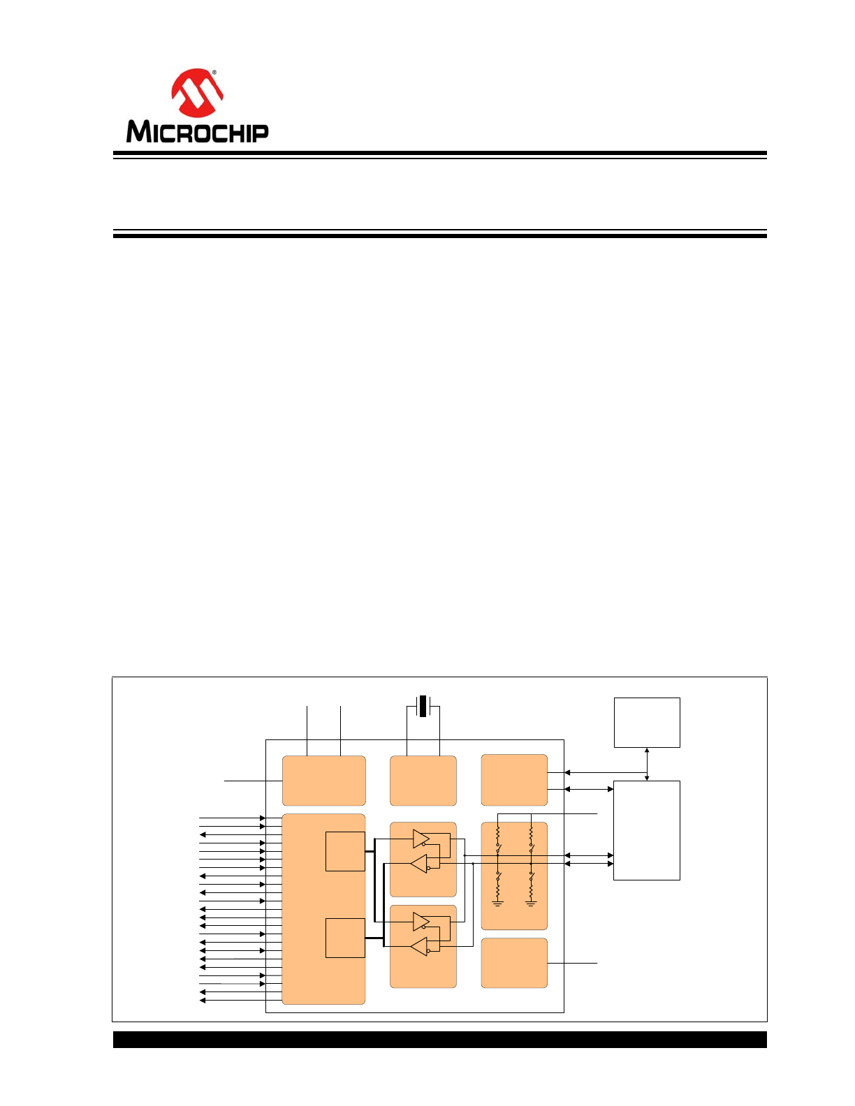
Functional Overview
The USB3500 is a highly integrated USB transceiver
system. It contains a complete USB 2.0 PHY with the
UTMI+ industry standard interface to support fast time
to market for a USB controller. The USB3500 is com-
posed of the functional blocks shown in the figure
below.
USB3500 Block Diagram
UTMI+
Digital
OTG
Module
24 MHz
XTAL
Internal
Regulators
& POR
5V
Power
Supply
Bias
Gen.
XCVRSEL[1:0]
VDD3.3
XTAL &
PLL
XI
VBUS
ID
VDD3.3
DP
DM
USB3500
VD
D1.8
VD
DA
1
.8
m
XO
RBIAS
Mini-AB
USB
Connector
HS XCVR
FS/LS
XCVR
Resistors
Rp
u_
d
p
R
p
d
_dm
Rpd
_
dp
Rpu_d
m
TERMSEL
TXREADY
SUSPENDN
TXVALID
RESET
CHRGVBUS
RXACTIVE
OPMODE[1:0]
ID_DIG
IDPULLUP
CLKOUT
LINESTATE[1:0]
HOSTDISC
DISCHRGVBUS
SESSEND
DATA[7:0]
RXVALID
SESSVLD
DPPD
DMPD
RXERROR
VBUSVLD
TX
Logic
RX
Logic
USB3500
Hi-Speed USB Host, Device or OTG PHY
With UTMI+ Interface

USB3500
DS00002103A-page 2
2005 - 2016 Microchip Technology Inc.
TO OUR VALUED CUSTOMERS
It is our intention to provide our valued customers with the best documentation possible to ensure successful use of your Microchip
products. To this end, we will continue to improve our publications to better suit your needs. Our publications will be refined and
enhanced as new volumes and updates are introduced.
If you have any questions or comments regarding this publication, please contact the Marketing Communications Department via
E-mail at
docerrors@microchip.com
. We welcome your feedback.
Most Current Data Sheet
To obtain the most up-to-date version of this data sheet, please register at our Worldwide Web site at:
http://www.microchip.com
You can determine the version of a data sheet by examining its literature number found on the bottom outside corner of any page.
The last character of the literature number is the version number, (e.g., DS30000000A is version A of document DS30000000).
Errata
An errata sheet, describing minor operational differences from the data sheet and recommended workarounds, may exist for cur-
rent devices. As device/documentation issues become known to us, we will publish an errata sheet. The errata will specify the
revision of silicon and revision of document to which it applies.
To determine if an errata sheet exists for a particular device, please check with one of the following:
• Microchip’s Worldwide Web site;
http://www.microchip.com
• Your local Microchip sales office (see last page)
When contacting a sales office, please specify which device, revision of silicon and data sheet (include -literature number) you are
using.
Customer Notification System
Register on our web site at
www.microchip.com
to receive the most current information on all of our products.

2005 - 2016 Microchip Technology Inc.
DS00002103A-page 3
USB3500
Table of Contents
1.0 General Description ........................................................................................................................................................................ 4
2.0 Pin Configuration and Pin Definitions ............................................................................................................................................. 6
3.0 Limiting Values .............................................................................................................................................................................. 11
4.0 Electrical Characteristics ............................................................................................................................................................... 12
5.0 Detailed Functional Description .................................................................................................................................................... 16
6.0 Application Notes .......................................................................................................................................................................... 25
7.0 Package Outline ............................................................................................................................................................................ 39
Appendix A: Revision History .............................................................................................................................................................. 41
The Microchip Web Site ...................................................................................................................................................................... 42
Customer Change Notification Service ............................................................................................................................................... 42
Customer Support ............................................................................................................................................................................... 42
Product Identification System ............................................................................................................................................................. 43
USB3500
DS00002103A-page 4
2005 - 2016 Microchip Technology Inc.
1.0
GENERAL DESCRIPTION
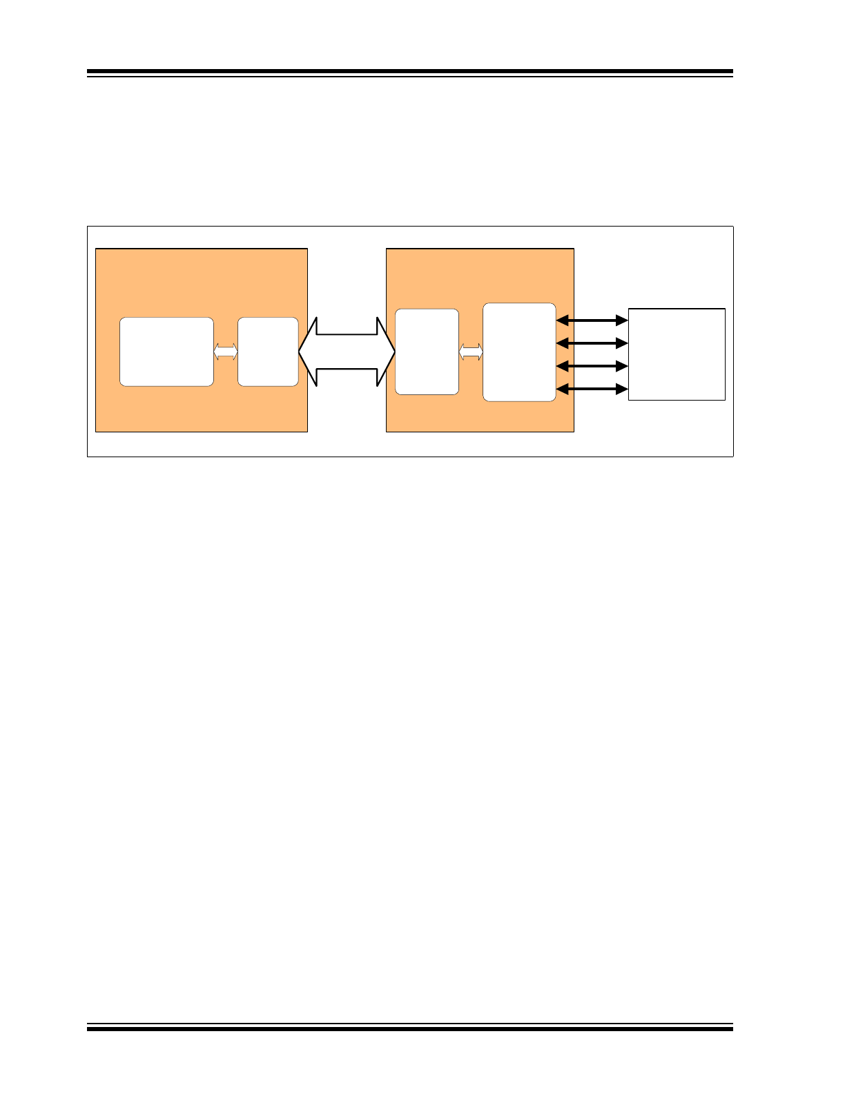
The USB3500 is a stand-alone Hi-Speed USB Physical Layer Transceiver (PHY). The USB3500 uses a UTMI+ interface
to connect to an SOC or FPGA or custom ASIC. The USB3500 provides a flexible alternative to integrating the analog
PHY block for new designs.
The USB3500 provides a fully compliant USB 2.0 interface, and supports High-Speed (HS), Full-Speed (FS), and Low-
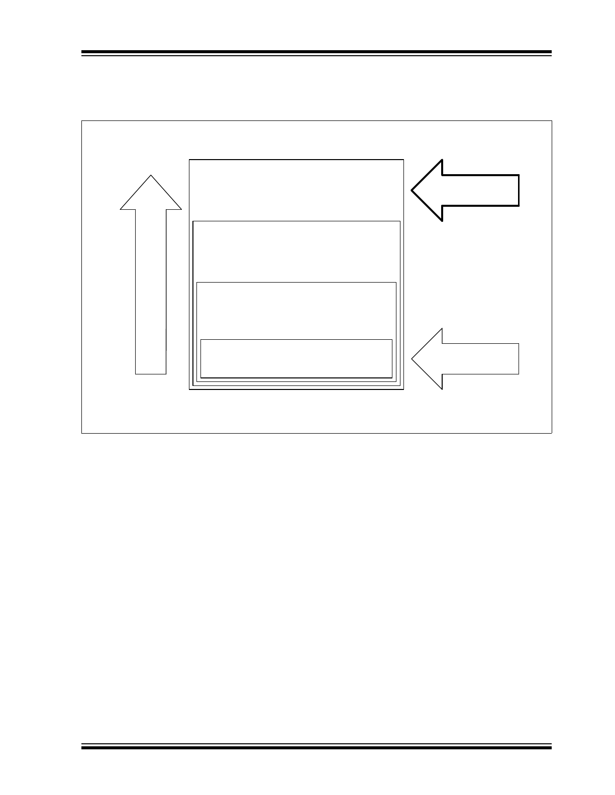
Speed (LS) USB. The USB3500 supports all levels of the UTMI+ specification as shown in
Figure 1-2
.
The USB3500 can also, as an option, fully support the On-the-Go (OTG) protocol defined in the On-The-Go Supplement
to the USB 2.0 Specification. On-the-Go allows the Link to dynamically configure the USB3500 as host or peripheral
configured dynamically by software. For example, a cell phone may connect to a computer as a peripheral to exchange
address information or connect to a printer as a host to print pictures. Finally the OTG enabled device can connect to
another OTG enabled device to exchange information. All this is supported using a single low profile Mini-AB USB con-
nector.
Designs not needing OTG can ignore the OTG feature set.
FIGURE 1-1:
BASIC UTMI+ USB DEVICE BLOCK DIAGRAM
SOC/FPGA/ASIC
Including Device Controller
USB3500
USB 2.0
Analog
w/ OTG
USB
Connector
(Standard
or Mini)
DM
V
BUS
DP
ID
Hi-Speed
USB App.
UTMI+
Interface
UTMI+
Digital
Logic
UTMI+
Link
2005 - 2016 Microchip Technology Inc.
DS00002103A-page 5
USB3500
The USB3500 uses Microchip’s advanced proprietary technology to minimize power dissipation, resulting in maximized
battery life in portable applications.
1.1
Applications
The USB3500 is targeted for any application where a hi-speed USB connection is desired.
The USB3500 is well suited for:
• Cell Phones
• MP3 Players
• Scanners
• Printers
• External Hard Drives
• Still and Video Cameras
• Portable Media Players
• Entertainment Devices
1.2
Reference Documents
• Universal Serial Bus Specification, Revision 2.0, April 27, 2000
• USB 2.0 Transceiver Macrocell Interface (UTMI) Specification, Version 1.02, May 27, 2000
• On-The-Go Supplement to the USB 2.0 Specification, Revision 1.0a, June 24, 2003
• UTMI+ Specification, Revision 1.0, February 2, 2004
FIGURE 1-2:
UTMI+ LEVEL 3 SUPPORT
UTMI+ Level 0
USB2.0 Peripherals Only
A
D
D
E
D FEAT
UR
ES
USB3500
UTMI+ Level 3
USB2.0 Peripheral, host controllers, On-the-
Go devices
(HS, FS, LS, preamble packet)
UTMI+ Level 2
USB2.0 Peripheral, host controllers, On-
the-Go devices
(HS, FS, and LS but no preamble packet)
UTMI+ Level 1
USB2.0 Peripheral, host controllers, and
On-the-Go devices
(HS and FS Only)
USB3280
USB3250
USB3500
DS00002103A-page 6
2005 - 2016 Microchip Technology Inc.
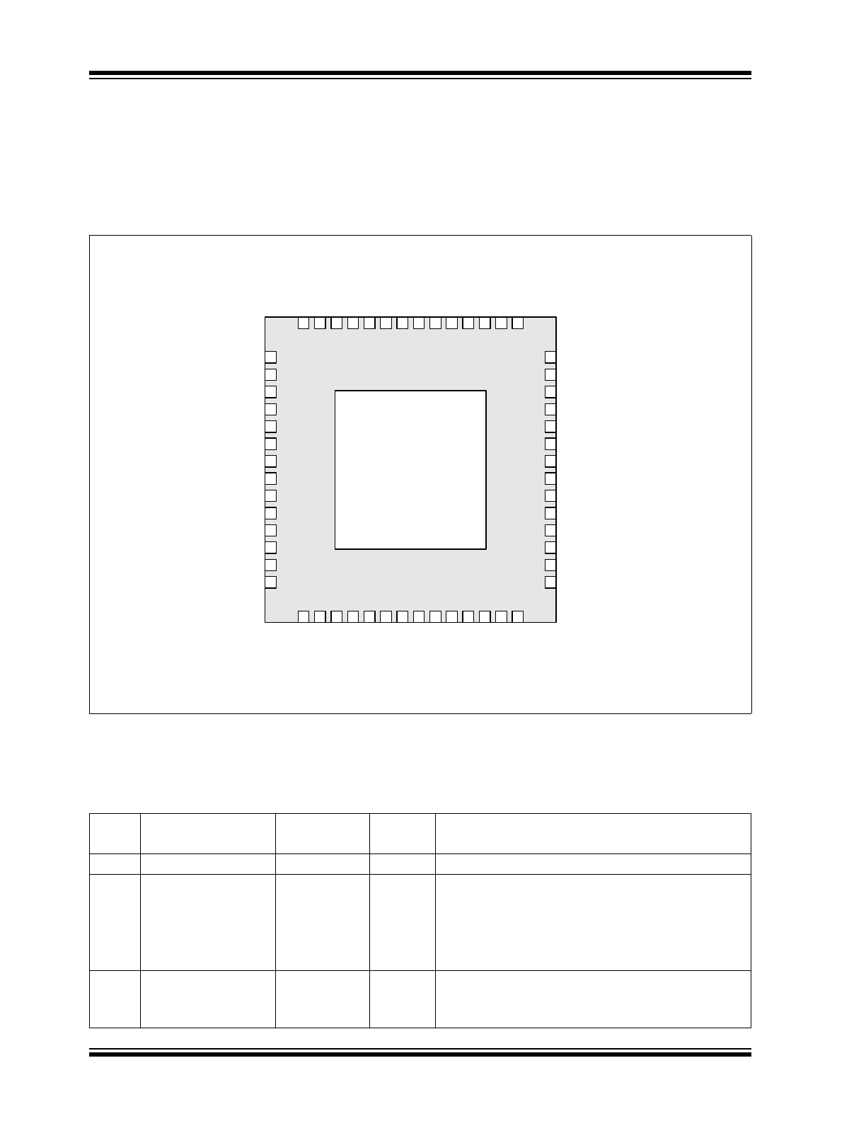
2.0
PIN CONFIGURATION AND PIN DEFINITIONS
The USB3500 is offered in a 56-pin QFN package. The pin definitions and locations are documented below.
2.1
USB3500 Pin Locations
The flag of the QFN package must be connected to ground with a via array.
2.2
Pin Definitions
FIGURE 2-1:
USB3500 PINOUT - TOP VIEW
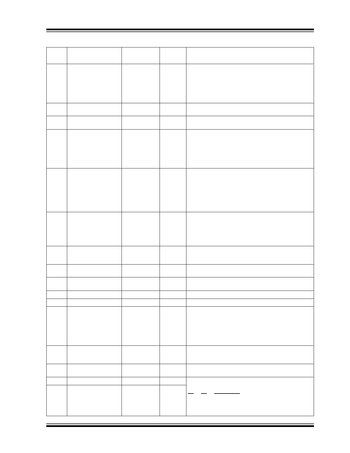
TABLE 2-1:
USB3500 PIN DEFINITIONS
Pin
Name
Direction,
Type
Active
Level
Description
1
VSS
Ground
N/A
PHY ground.
2
XCVRSEL[0]
Input
N/A
Transceiver Select. These signals select between the
FS and HS transceivers:
Transceiver select.
00: HS
01: FS
10: LS
11: LS data, FS rise/fall times
3
TERMSEL
Input
N/A
Termination Select. This signal selects between the
FS and HS terminations:
0: HS termination enabled
1: FS termination enabled
ID
P
U
L
L
U
P
XCVRS
E
L
1
L
INE
ST
ATE[
0
]
L
INE
ST
ATE[
1
]
OP
M
O
DE
[1
]
OP
M
O
DE
[0
]
CH
RGV
B
US
RX
A
C
T
IV
E
ID
_
D
IG
VS
S
CL
KOU
T
VS
S
VDD1
.8
VDD3
.3
SESSVLD
DATA[1]
DATA[0]
DATA[2]
DATA[3]
DATA[4]
DATA[5]
DATA[6]
DATA[7]
RXVALID
VSS
SESSEND
DISCHRGVBUS
HOSTDISC
RBI
A
S
VDD3.
3
VDD3.
3
VDDA1
.8
XI
XO
VS
S
VDD1.
8
VB
USVL
D
VDD3.
3
VS
S
RXE
R
ROR
DM
PD
DPP
D
VSS
DM
DP
VDD3.3
VSS
VDD3.3
RESET
TXVALID
SUSPENDN
ID
VBUS
TXREADY
TERMSEL
XCVRSEL0
10
11
12
13
14
15
16
17
18
19
20
21
22
23
24
25
26
27
28
42
41
29
30
31
32
34
35
36
37
38
39
40
33
48
47
46
45
44
43
56
55
54
53
52
51
50
49
1
2
3
4
5
6
7
8
9
USB3500
Hi-Speed USB
UTMI+ PHY
56 Pin QFN
GND FLAG
2005 - 2016 Microchip Technology Inc.
DS00002103A-page 7
USB3500
4
TXREADY
Output
High
Transmit Data Ready. If TXVALID is asserted, the Link
must always have data available for clocking into the
TX Holding Register on the rising edge of CLKOUT.
TXREADY is an acknowledgment to the Link that the
transceiver has clocked the data from the bus and is
ready for the next transfer on the bus. If TXVALID is
negated, TXREADY can be ignored by the Link.
5
VBUS
I/O,
Analog
N/A
VBUS pin of the USB cable.
6
ID
Input,
Analog
N/A
ID pin of the USB cable.
7
SUSPENDN
Input
Low
Suspend. Places the transceiver in a mode that draws
minimal power from supplies. In host mode, R
PU
is
removed during suspend. In device mode, R
PD
is
controlled by TERMSEL. In suspend mode the clocks
are off.
0: PHY in suspend mode
1: PHY in normal operation
8
TXVALID
Input
High
Transmit Valid. Indicates that the DATA bus is valid for
transmit. The assertion of TXVALID initiates the
transmission of SYNC on the USB bus. The negation
of TXVALID initiates EOP on the USB.
Control inputs (OPMODE[1:0],
TERMSEL,XCVERSEL) must not be changed on the
de-assertion or assertion of TXVALID.
9
RESET
Input
High
Reset. Reset all state machines. After coming out of
reset, must wait 5 rising edges of clock before
asserting TXValid for transmit.
Assertion of Reset: May be asynchronous to CLKOUT
De-assertion of Reset: Must be synchronous to
CLKOUT
10
VDD3.3
N/A
N/A
3.3V PHY Supply. Provides power for USB 2.0
Transceiver, UTMI+ Digital, Digital I/O, and
Regulators.
11
DP
I/O,
Analog
N/A
D+ pin of the USB cable.
12
DM
I/O,
Analog
N/A
D- pin of the USB cable.
13
VSS
Ground
N/A
PHY ground.
14
VDD3.3
N/A
N/A
3.3V PHY Supply.
15
XCVRSEL[1]
Input
N/A
Transceiver Select. These signals select between the
FS and HS transceivers:
Transceiver select.
00: HS
01: FS
10: LS
11: LS data, FS rise/fall times
16
CHRGVBUS
Input
High
Charge VBUS through a resistor to VDD3.3.
0: do not charge VBUS
1: charge VBUS
17
RXACTIVE
Output
High
Receive Active. Indicates that the receive state
machine has detected Start of Packet and is active.
18
OPMODE[1]
Input
N/A
Operational Mode. These signals select between the
various operational modes:
[1] [0] Description
0 0 0: Normal Operation
0 1 1: Non-driving (all terminations removed)
1 0 2: Disable bit stuffing and NRZI encoding
1 1 3: Reserved
19
OPMODE[0]
Input
N/A
TABLE 2-1:
USB3500 PIN DEFINITIONS (CONTINUED)
Pin
Name
Direction,
Type
Active
Level
Description
USB3500
DS00002103A-page 8
2005 - 2016 Microchip Technology Inc.
20
ID_DIG
Output
High
ID Digital. Indicates the state of the ID pin.
0: connected plug is a mini-A
1: connected plug is a mini-B
21
IDPULLUP
Input
High
ID Pull-up. Enables sampling of the analog ID line.
Disabling the ID line sampler will reduce PHY power
consumption.
0: Disable sampling of ID line.
1: Enable sampling of ID line.
22
VSS
Ground
N/A
PHY ground.
23
CLKOUT
Output,
CMOS
N/A
60MHz reference clock output. All UTMI+ signals are
driven synchronous to this clock.
24
VSS
Ground
N/A
PHY ground.
25
LINESTATE[1]
Output
N/A
Line State. These signals reflect the current state of
the USB data bus in FS mode. Bit [0] reflects the state
of DP and bit [1] reflects the state of DM. When the
device is suspended or resuming from a suspended
state, the signals are combinatorial. Otherwise, the
signals are synchronized to CLKOUT.
[1] [0] Description
0 0 0: SEO
0 1 1: J State
1 0 2: K State
1 1 3: SE1
26
LINESTATE[0]
Output
N/A
27
VDD1.8
N/A
N/A
1.8V regulator output for digital circuitry on chip. Place
a 0.1uF capacitor near this pin and connect the
capacitor from this pin to ground. Connect pin 27 to
pin 49.
28
VDD3.3
N/A
N/A
3.3V PHY Supply. Provides power for USB 2.0
Transceiver, UTMI+ Digital, Digital I/O, and
Regulators.
29
HOSTDISC
Output
High
Host Disconnect. In HS Host mode this indicates to
that a downstream device has been disconnected.
Automatically reset to 0b when Low Power Mode is
entered.
30
DISCHRGVBUS
Input
High
Discharge VBUS through a resistor to ground.
0: do not discharge VBUS
1: discharge VBUS
31
SESSEND
Output
High
Session End. Indicates that the voltage on Vbus is
below its B-Device Session End threshold.
0: VBUS > V
SessEnd
1: VBUS < V
SessEnd
TABLE 2-1:
USB3500 PIN DEFINITIONS (CONTINUED)
Pin
Name
Direction,
Type
Active
Level
Description
2005 - 2016 Microchip Technology Inc.
DS00002103A-page 9
USB3500
32
DATA[7]
I/O,
CMOS,
Pull-low
N/A
8-bit bi-directional data bus. Data[7] is the MSB and
Data[0] is the LSB.
33
DATA[6]
I/O,
CMOS,
Pull-low
N/A
34
DATA[5]
I/O,
CMOS,
Pull-low
N/A
35
DATA[4]
I/O,
CMOS,
Pull-low
N/A
36
DATA[3]
I/O,
CMOS,
Pull-low
N/A
37
DATA[2]
I/O,
CMOS,
Pull-low
N/A
38
DATA[1]
I/O,
CMOS,
Pull-low
N/A
39
DATA[0]
I/O,
CMOS,
Pull-low
N/A
40
VSS
Ground
N/A
PHY ground.
41
RXVALID
Output
High
Receive Data Valid. Indicates that the DATA bus has
received valid data. The Receive Data Holding
Register is full and ready to be unloaded. The Link is
expected to register the DATA bus on the next rising
edge of CLKOUT.
42
SESSVLD
Output
High
Session Valid. Indicates that the voltage on Vbus is
above the indicated threshold.
0: VBUS < V
SessVld
1: VBUS > V
SessVld
43
DPPD
Input
N/A
DP Pull-down Select. This signal enables the 15k
Ohm pull-down resistor on the DP line.
0: Pull-down resistor not connected to DP
1: Pull-down resistor connected to DP
44
DMPD
Input
N/A
DM Pull-down Select. This signal enables the 15k
Ohm pull-down resistor on the DM line.
0: Pull-down resistor not connected to DM
1: Pull-down resistor connected to DM
45
RXERROR
Output
High
Receive Error. This output is clocked with the same
timing as the receive DATA lines and can occur at
anytime during a transfer.
0: Indicates no error.
1: Indicates a receive error has been detected.
46
VSS
Ground
N/A
PHY ground.
47
VBUSVLD
Output
High
VBUS Valid. Indicates that the voltage on Vbus is
above the indicated threshold.
0: VBUS < V
VbusVld
1: VBUS > V
VbusVld
48
VDD3.3
N/A
N/A
3.3V PHY Supply. Provides power for USB 2.0
Transceiver, UTMI+ Digital, Digital I/O, and
Regulators.
TABLE 2-1:
USB3500 PIN DEFINITIONS (CONTINUED)
Pin
Name
Direction,
Type
Active
Level
Description
USB3500
DS00002103A-page 10
2005 - 2016 Microchip Technology Inc.
49
VDD1.8
N/A
N/A
1.8V regulator output for digital circuitry on chip. Place
a 4.7uF low ESR capacitor near this pin and connect
the capacitor from this pin to ground. Connect pin 49
to pin 27. See
Section 5.6, "Internal Regulators and
POR," on page 22
.
50
VSS
Ground
N/A
PHY ground.
51
XO
Output,
Analog
N/A
Crystal pin. If using an external clock on XI this pin
should be floated.
52
XI
Input,
Analog
N/A
Crystal pin. A 24MHz crystal is supported. The crystal
is placed across XI and XO. An external 24MHz clock
source may be driven into XI in place of a crystal.
53
VDDA1.8
N/A
N/A
1.8V regulator output for analog circuitry on chip.
Place a 0.1uF capacitor near this pin and connect the
capacitor from this pin to ground. In parallel, place a
4.7uF low ESR capacitor near this pin and connect the
capacitor from this pin to ground. See
Section 5.6,
"Internal Regulators and POR"
.
54
VDD3.3
N/A
N/A
3.3V PHY Supply. Provides power for USB 2.0
Transceiver, UTMI+ Digital, Digital I/O, and
Regulators.
55
VDD3.3
N/A
N/A
3.3V PHY Supply. Should be connected directly to pin
54.
56
RBIAS
Analog,
CMOS
N/A
External 1% bias resistor. Requires a 12KΩ resistor to
ground.
GND FLAG
Ground
N/A
Ground. The flag must be connected to the ground
plane.
TABLE 2-1:
USB3500 PIN DEFINITIONS (CONTINUED)
Pin
Name
Direction,
Type
Active
Level
Description