

2012 - 2015 Microchip Technology Inc.
DS00001915B-page 1
Highlights
• USB-IF Battery Charging 1.1 Specification Com-
pliant
• Link Power Management (LPM) Specification
Compliant
• Integrated ESD protection circuits
- Up to ±25kV IEC Air Discharge without exter-
nal devices
• Over-Voltage Protection circuit (OVP) protects the
VBUS pin from continuous DC voltages up to 30V
• Microchip RapidCharge Anywhere™ Provides:
- 3-times the charging current through a USB
port over traditional solutions
- USB-IF Battery Charging 1.1 compliance to
any portable device
- Charging current up to 1.5Amps via compati-
ble USB host or dedicated charger
- Dedicated Charging Port (DCP), Charging
(CDP) & Standard (SDP) Downstream Port
support
• flexPWR
®
Technology
- Extremely low current design ideal for battery
powered applications
- “Sleep” mode tri-states all ULPI pins and
places the part in a low current state
- 1.8V to 3.3V IO Voltage
• Single Power Supply Operation
- Integrated 1.8V regulator
- Integrated 3.3V regulator
- 100mV dropout voltage
• PHYBoost
- Programmable USB transceiver drive
strength for recovering signal integrity
• VariSense
TM
- Programmable USB receiver sensitivity
• “Wrapper-less” design for optimal timing perfor-
mance and design ease
- Low Latency Hi-Speed Receiver (43 Hi-
Speed clocks Max) allows use of legacy
UTMI Links with a ULPI bridge
• External Reference Clock operation available
- 19.2MHz Reference Clock needed
- ULPI Clock Input Mode (60MHz sourced by
Link)
- 0 to 3.6V input drive tolerant
- Able to accept “noisy” clock sources as refer-
ence to internal, low-jitter PLL
- Crystal support available
• Smart detection circuits allow identification of
USB charger, headset, or data cable insertion
• Includes full support for the optional On-The-Go
(OTG) protocol detailed in the On-The-Go Sup-
plement Revision 2.0 specification
• Supports the OTG Host Negotiation Protocol
(HNP) and Session Request Protocol (SRP)
• UART mode for non-USB serial data transfers
• Internal 5V cable short-circuit protection of ID, DP
and DM lines to VBUS or ground
• Industrial Operating Temperature -40
°C to +85°C
• 32 pin, QFN RoHS Compliant package
(5 x 5x 0.90 mm height)
Applications
The USB3370 is the solution of choice for any applica-
tion where a Hi-Speed USB connection is desired and
when board space, power, and interface pins must be
minimized.
• Cell Phones
• PDAs
• MP3 Players
• GPS Personal Navigation
• Scanners
• External Hard Drives
• Digital Still and Video Cameras
• Portable Media Players
• Entertainment Devices
• Printers
• Set Top Boxes
• Video Record/Playback Systems
• IP and Video Phones
• Gaming Consoles
USB3370
Enhanced Single Supply Hi-Speed USB ULPI Transceiver

USB3370
DS00001915B-page 2
2012 - 2015 Microchip Technology Inc.
TO OUR VALUED CUSTOMERS
It is our intention to provide our valued customers with the best documentation possible to ensure successful use of your Microchip
products. To this end, we will continue to improve our publications to better suit your needs. Our publications will be refined and
enhanced as new volumes and updates are introduced.
If you have any questions or comments regarding this publication, please contact the Marketing Communications Department via
E-mail at
docerrors@microchip.com
. We welcome your feedback.
Most Current Data Sheet
To obtain the most up-to-date version of this data sheet, please register at our Worldwide Web site at:
http://www.microchip.com
You can determine the version of a data sheet by examining its literature number found on the bottom outside corner of any page.
The last character of the literature number is the version number, (e.g., DS30000000A is version A of document DS30000000).
Errata
An errata sheet, describing minor operational differences from the data sheet and recommended workarounds, may exist for cur-
rent devices. As device/documentation issues become known to us, we will publish an errata sheet. The errata will specify the
revision of silicon and revision of document to which it applies.
To determine if an errata sheet exists for a particular device, please check with one of the following:
• Microchip’s Worldwide Web site;
http://www.microchip.com
• Your local Microchip sales office (see last page)
When contacting a sales office, please specify which device, revision of silicon and data sheet (include -literature number) you are
using.
Customer Notification System
Register on our web site at
www.microchip.com
to receive the most current information on all of our products.

2012 - 2015 Microchip Technology Inc.
DS00001915B-page 3
USB3370
Table of Contents
1.0 Introduction ..................................................................................................................................................................................... 4
2.0 USB3370 Pin Locations and Definitions ......................................................................................................................................... 6
3.0 Limiting Values ................................................................................................................................................................................ 9
4.0 Electrical Characteristics ............................................................................................................................................................... 10
5.0 Architecture Overview ................................................................................................................................................................... 17
6.0 ULPI Operation ............................................................................................................................................................................. 33
7.0 ULPI Register Map ........................................................................................................................................................................ 51
8.0 Application Notes .......................................................................................................................................................................... 61
9.0 Package Outline ............................................................................................................................................................................ 66
Appendix A: Data Sheet Revision History ........................................................................................................................................... 71
The Microchip Web Site ...................................................................................................................................................................... 72
Customer Change Notification Service ............................................................................................................................................... 72
Customer Support ............................................................................................................................................................................... 72
Product Identification System ............................................................................................................................................................. 73

USB3370
DS00001915B-page 4
2012 - 2015 Microchip Technology Inc.
1.0
INTRODUCTION
Microchip’s USB3370 is a family of Hi-Speed USB 2.0 Transceivers that provide a physical layer (PHY) solution well-
suited for portable electronic devices. Both commercial and industrial temperature applications are supported.
Several advanced features make the USB3370 the transceiver of choice by reducing both eBOM part count and printed
circuit board (PCB) area. Outstanding ESD robustness eliminates the need for external ESD protection devices in typ-
ical applications. The internal Over-Voltage Protection circuit (OVP) protects the USB3370 from voltages up to 30V on
the VBUS pin. By using a reference clock from the Link, the USB3370 removes the cost of a dedicated crystal reference
from the design. The USB3370 includes integrated 3.3V and 1.8V regulators, making it possible to operate the device
from a single power supply.
The USB3370 is optimized for use in portable applications where a low operating current and standby currents are
essential. The USB3370 operates from a single supply and includes integrated regulators for its supplies. The USB3370
also supports the USB Link Power Management protocol (LPM) to further reduce USB operating currents.
The USB3370 also includes family is enabled with Microchip's RapidCharge Anywhere
TM
which supports USB-IF Bat-
tery Charging 1.1 for any portable device. RapidCharge Anywhere
TM
provides three times the charging current through
a USB port over traditional solutions which translate up to 1.5Amps via compatible USB host or dedicated charger. In
addition, this provides a complete USB charging ecosystem between device and host ports such as Dedicated Charging
Port (DCP), Charging (CDP) and Standard (SDP) Downstream Ports.
Section 5.9
describes this is further detail.
The USB3370 meets all of the electrical requirements for a Hi-Speed USB Host, Device, or an On-the-Go (OTG) trans-
ceiver. In addition to the supporting USB signaling, the USB3370 also provides USB UART mode.
USB3370 uses the industry standard UTMI+ Low Pin Interface (ULPI) to connect the USB transceiver to the Link. ULPI
uses a method of in-band signaling and status byte transfers between the Link and PHY to facilitate a USB session with
only twelve pins.
The USB3370 uses Microchip’s “wrapper-less” technology to implement the ULPI interface. This “wrapper-less” tech-
nology allows the PHY to achieve a low latency transmit and receive time. Microchip’s low latency transceiver allows an
existing UTMI Link to be reused by adding a UTMI to ULPI bridge. By adding a bridge to the ASIC the existing and
proven UTMI Link IP can be reused.
2012 - 2015 Microchip Technology Inc.
DS00001915B-page 5
USB3370
The USB3370 includes an integrated 3.3V LDO regulator that is used to generate 3.3V from power applied to the VBAT
pin. The voltage on the VBAT pin can range from 3.0 to 5.5V. The regulator dropout voltage is less than 100mV which
allows the PHY to continue USB signaling when the voltage on VBAT drops to 3.0V. The USB transceiver will continue
to operate at lower voltages, although some parameters may be outside the limits of the USB specifications. The VBAT
and VDD33 pins should never be connected together.
In USB UART mode, the USB3370 DP and DM pins are redefined to enable pass-through of asynchronous serial data.
The USB3370 will enter UART mode when programmed, as described in
Section 6.7.1
.
1.1
Reference Documents
UTMI+ Low Pin Interface (ULPI) Specification, Rev. 1.1
Universal Serial Bus Specification, Revision 2.0
On-The-Go Supplement to the USB2.0 Specification, Rev. 1.3
On-The-Go Supplement to the USB2.0 Specification, Rev. 2.0
USB Battery Charging Specification, Rev. 1.1
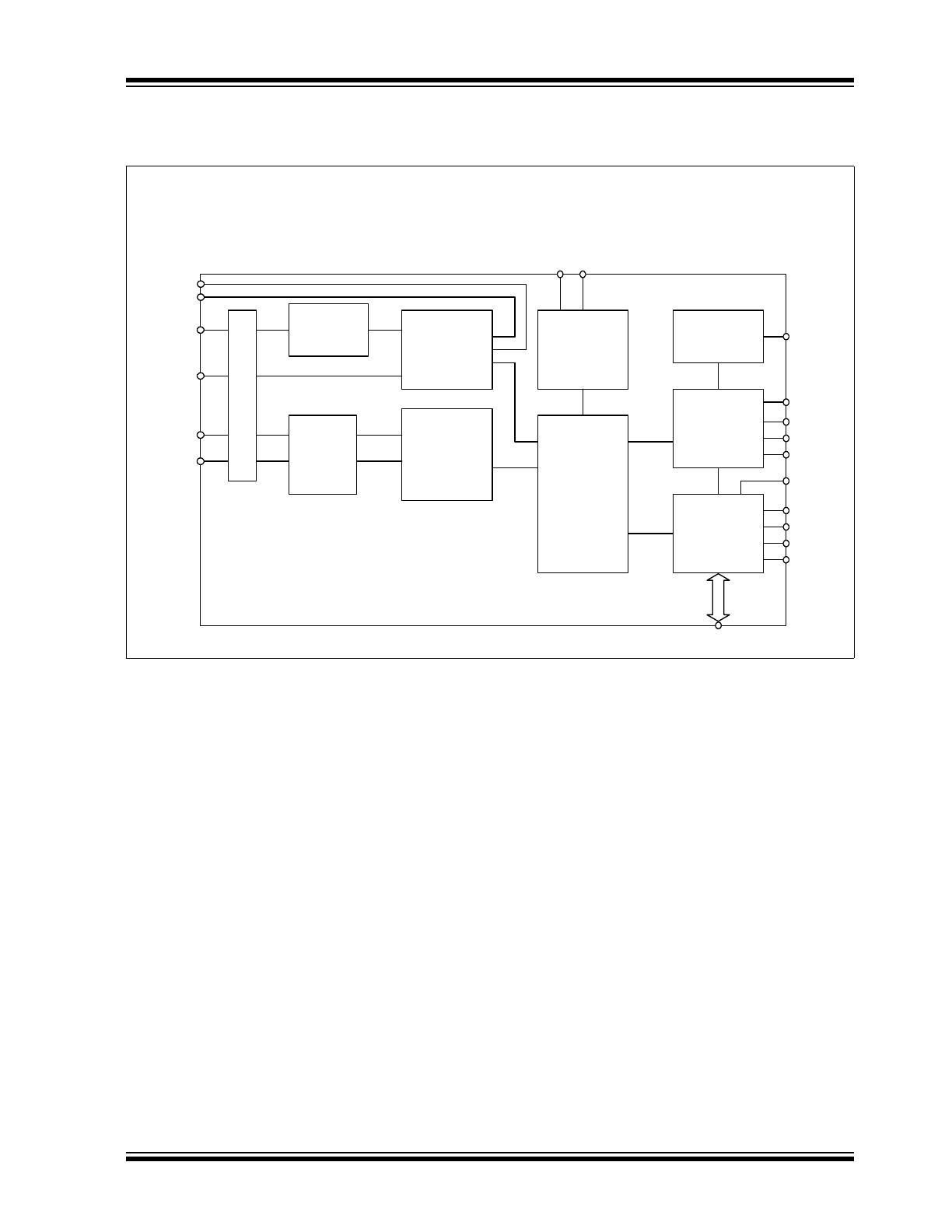
FIGURE 1-1:
BLOCK DIAGRAM USB3370
OTG
Hi-Speed
USB
Transceiver
ULPI
Interface
ULPI
Registers
and State
Machine
BIAS
Low Jitter
Integrated
PLL
Integrated
Power
Management
VBUS
ID
DP
DM
RBIAS
ESD Prot
ectio
n
RE
F
C
LK
/
XI
DATA[7:0]
RESETB
VDD18
VDD33
VBAT
DIR
NXT
STP
CLKOUT
OVP
VDDIO
XO
CPEN_N
BC 1.1
EXTVBUS
USB3370
DS00001915B-page 6
2012 - 2015 Microchip Technology Inc.
2.0
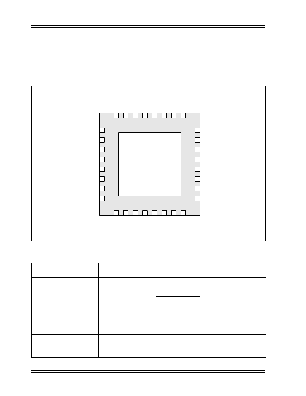
USB3370 PIN LOCATIONS AND DEFINITIONS
2.1
USB3370
Pin Locations and Descriptions
2.1.1
USB3370 PIN DIAGRAM AND PIN DEFINITIONS
The illustration below is viewed from the top of the package.
The following table details the pin definitions for the figure above.
FIGURE 2-1:
USB3370 PIN LOCATIONS - TOP VIEW
TABLE 2-1:
USB3370 PIN DESCRIPTIONS
Pin
Name
Direction/
Type
Active
Level
Description
27
CLKOUT
Output,
CMOS
N/A
ULPI Clock Out Mode:
60MHz ULPI clock output. All ULPI signals are driven
synchronous to the rising edge of this clock.
ULPI Clock In Mode:
Connect this pin to VDDIO to configure 60MHz ULPI
Clock IN mode as described in
Section 5.5.1
.
21
NXT
Output,
CMOS
High
The PHY asserts NXT to throttle the data. When the
Link is sending data to the PHY, NXT indicates when
the current byte has been accepted by the PHY.
1
DATA[0]
I/O,
CMOS
N/A
ULPI bi-directional data bus. DATA[0] is the LSB.
32
DATA[1]
I/O,
CMOS
N/A
ULPI bi-directional data bus.
31
DATA[2]
I/O,
CMOS
N/A
ULPI bi-directional data bus.
USB3300
Hi-Speed USB2
ULPI PHY
32 Pin QFN
1
2
3
4
5
6
7
8
32 Pin QFN
5x5 mm
GND FLAG
9
10
11
12
13
14
15
16
24
23
22
21
20
19
18
17
32
31
30
29
28
27
26
25
VDDIO
RBIAS
DP
EXTVBUS
DM
DATA0
VDDIO
DATA7
STP
DIR
VDD18
NXT
ID
NC
VBUS
NC
D
A
TA1
GND
V
DD33
VBAT
C
PEN_N
REFCLK
XO
RESETB
DATA
2
NC
DATA6
VDD
IO
DAT
A
4
CLK
O
UT
DAT
A
3
DAT
A
5
2012 - 2015 Microchip Technology Inc.
DS00001915B-page 7
USB3370
28
DATA[3]
I/O,
CMOS
N/A
ULPI bi-directional data bus.
26
DATA[4]
I/O,
CMOS
N/A
ULPI bi-directional data bus.
6
EXTVBUS
Input, CMOS
High
External Vbus Detect. Connect to fault output of an
external USB power switch or an external Vbus Valid
comparator. See
Section 5.7.5, "External Vbus
Indicator," on page 29
for details. This pin has a pull
down resistor to prevent it from floating when the ULPI
bit UseExternalVbusIndicator is set to 0.
25
DATA[5]
I/O,
CMOS
N/A
ULPI bi-directional data bus.
24
DATA[6]
I/O,
CMOS
N/A
ULPI bi-directional data bus.
9
10
29
NC
N/A
N/A
No connect. Leave pin floating.
23
DATA[7]
I/O,
CMOS
N/A
ULPI bi-directional data bus. DATA[7] is the MSB.
12
CPEN_N
Output,
Open Drain
Low
External 5 volt supply enable. This pin is used to
enable the external Vbus power supply. The CPEN_N
pin is tri-stated on POR.
5
DP
I/O,
Analog
N/A
D+ pin of the USB cable.
4
DM
I/O,
Analog
N/A
D- pin of the USB cable.
14
VDD33
Power
N/A
3.3V Regulator Output. A 1.0uF (<1 ohm ESR) bypass
capacitor to ground is required for regulator stability.
The bypass capacitor should be placed as close as
possible to the USB3370.
11
VBAT
Power
N/A
Regulator input. The regulator supply can be from
5.5V to 3.0V.
13
VBUS
I/O,
Analog
N/A
This pin is used for the VBUS comparator inputs and
for VBUS pulsing during session request protocol. An
external resistor, R
VBUS
, is required between this pin
and the USB connector.
7
ID
Input,
Analog
N/A
For device applications the ID pin is connected to
VDD33
. For Host applications ID is grounded. For
OTG applications the ID pin is connected to the USB
connector.
3
RBIAS
Analog,
CMOS
N/A
Bias Resistor pin. This pin requires an 10kΩ (±1%)
resistor to ground, placed as close as possible to the
USB3370. Nominal voltage during ULPI operation is
0.8V.
16
XO
Output,
Analog
N/A
Crystal pin. If using an external clock on XI this pin
should be floated.
15
REFCLK
Input,
CMOS
N/A
ULPI Clock Out Mode:
Reference clock or XI (crystal in) pin.
ULPI Clock In Mode:
60MHz ULPI clock input.
TABLE 2-1:
USB3370 PIN DESCRIPTIONS (CONTINUED)
Pin
Name
Direction/
Type
Active
Level
Description

USB3370
DS00001915B-page 8
2012 - 2015 Microchip Technology Inc.
17
RESETB
Input,
CMOS,
Low
When low, the part is suspended and the 3.3V and
1.8V regulators are disabled. When high, the
USB3370 will operate as a normal ULPI device, as
described in
Section 5.6.2
. The state of this pin may
be changed asynchronously to the clock signals.
When asserted for a minimum of 1 microsecond and
then de-asserted, the ULPI registers are reset to their
default state and all internal state machines are reset.
18
VDD18
Power
N/A
1.8V Regulator Output. A 1.0uF (<1 ohm ESR) bypass
capacitor to ground is required for regulator stability.
The bypass capacitor should be placed as close as
possible to the USB3370.
20
STP
Input,
CMOS
High
The Link asserts STP for one clock cycle to stop the
data stream currently on the bus. If the Link is sending
data to the PHY, STP indicates the last byte of data
was on the bus in the previous cycle.
19
DIR
Output,
CMOS
N/A
Controls the direction of the data bus. When the PHY
has data to transfer to the Link, it drives DIR high to
take ownership of the bus. When the PHY has no data
to transfer it drives DIR low and monitors the bus for
commands from the Link.
2
22
30
VDDIO
Power
N/A
1.8V to 3.3V ULPI interface supply voltage.
FLAG
8
GND
Ground
N/A
Ground.
TABLE 2-1:
USB3370 PIN DESCRIPTIONS (CONTINUED)
Pin
Name
Direction/
Type
Active
Level
Description
2012 - 2015 Microchip Technology Inc.
DS00001915B-page 9
USB3370
3.0
LIMITING VALUES
3.1
Absolute Maximum Ratings
3.2
Recommended Operating Conditions
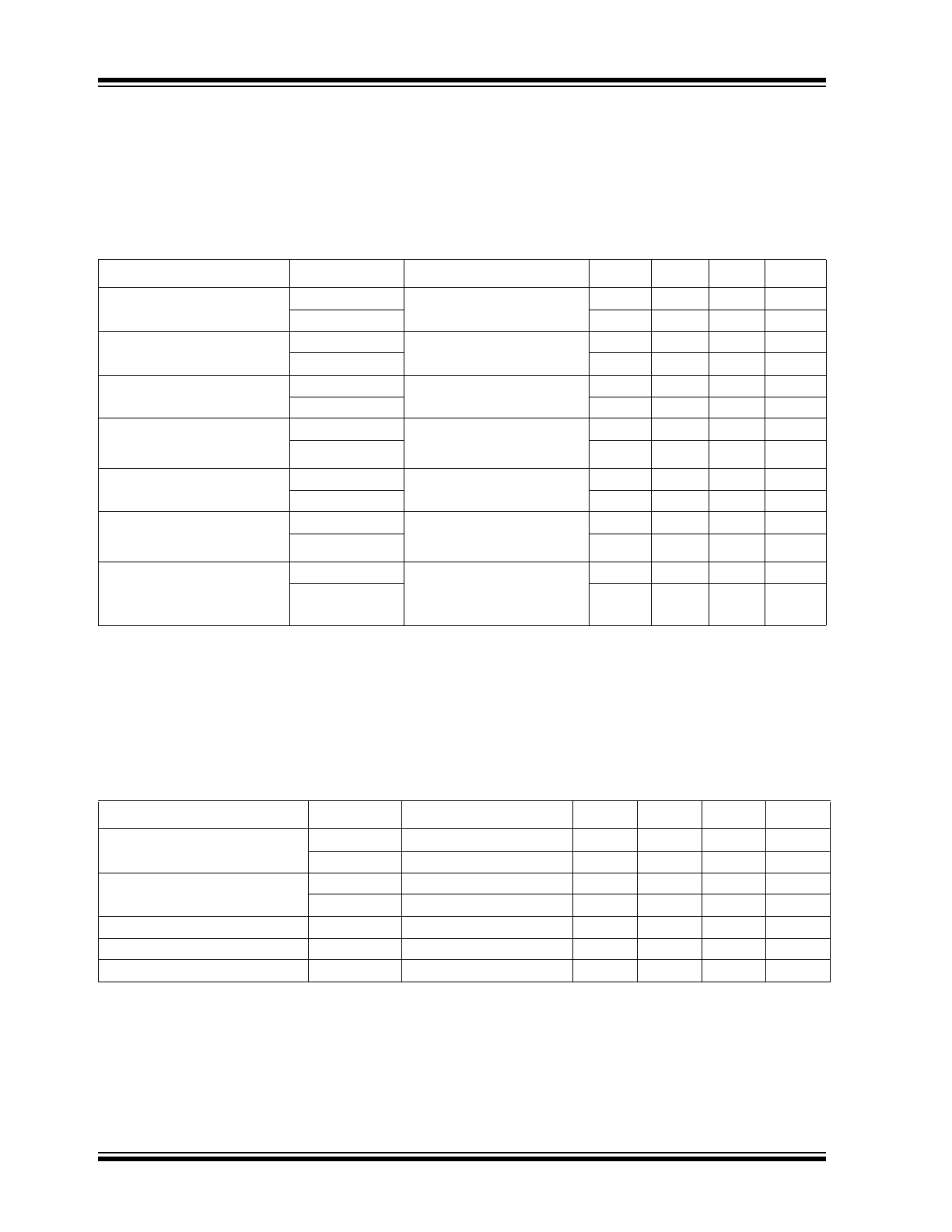
TABLE 3-1:
ABSOLUTE MAXIMUM RATINGS
Parameter
Symbol
Conditions
MIN
TYP MAX Units
VBUS
, VBAT, and ID,
voltage to GND
V
MAX_USB
Voltage measured at pin.
VBUS
tolerant to 30V with
external R
VBUS
.
-0.5
6.0
V
DP
and DM voltage to
GND
V
MAX_DPDM
-0.5
5.0
V
Maximum VDD18 voltage
to Ground
V
MAX_18V
-0.5
2.5
V
Maximum VDD33 voltage
to Ground
V
MAX_33V
-0.5
4.0
V
Maximum VDDIO voltage
to Ground
V
MAX_IOV
-0.5
4.0
Maximum I/O voltage to
Ground
V
MAX_IN
-0.5
V
DDIO
+ 0.7
Maximum I/O voltage to
Ground (EXTVBUS,
CPEN_N
)
V
MAX_IN
-0.5
5.5V
Operating Temperature
T
MAX_OP
-40
85
C
Storage Temperature
T
MAX_STG
-55
150
C
Note:
Stresses beyond those listed under “Absolute Maximum Ratings” may cause permanent damage to the
device. Exposure to absolute maximum rating conditions for extended periods may affect device reliability.
TABLE 3-2:
RECOMMENDED OPERATING CONDITIONS
Parameter
Symbol
Conditions
MIN
TYP MAX
Units
VBAT
to GND
V
BAT
3.0
5.5
V
VDD33
to GND
V
DD33
3.0
3.3
3.6
V
VDD18
to GND
V
DD18
1.6
1.8
2.0
V
VDDIO
to GND
V
DDIO
1.6
1.8-3.3
3.6
V
Input Voltage on Digital
Pins (RESETB, STP, DIR,
NXT
, DATA[7:0])
V
I
0.0
V
DDIO
V
Input Voltage on Digital
Pins (EXTVBUS,
CPEN_N
)
V
I
0.0
5.0
V
Voltage on Analog I/O
Pins (DP, DM, ID)
V
I(I/O)
0.0
V
DD33
V
VBUS
to GND
V
VMAX
0.0
5.5
Ambient Temperature
T
A
-40
85
C
USB3370
DS00001915B-page 10
2012 - 2015 Microchip Technology Inc.
4.0
ELECTRICAL CHARACTERISTICS
The following conditions are assumed unless otherwise specified:
V
DD33
= 3.0 to 3.6V; VDD18 = 1.6 to 2.0V; V
SS
= 0V; T
A
= -40C to +85C
4.1
Operating Current
Note 4-1
ClockSuspendM
bit = 0.
Note 4-2
SessEnd, VbusVld, and IdFloat comparators disabled. STP Interface protection disabled.
Note 4-3
REFCLK is OFF
4.2
Clock Specifications
The model number for each frequency of REFCLK is provided in
Product Identification System on page 73
.
Note 1:
T
START
and T
PREP
are measured from the time when REFCLK and RESETB are both valid to when the
USB3370 de-asserts DIR.
2:
The USB3370 uses the AutoResume feature,
Section 6.4.1.4
, to allow a host start-up time of less than 1ms.
Note 4-4
REFCLK with oscillator Input
Note 4-5
Crystal Input
TABLE 4-1:
OPERATING CURRENT
Parameter
Symbol
Conditions
MIN
TYP MAX Units
Synchronous Mode Current
(Default Configuration)
I
VBAT(SYNC)
USB Idle
24
27
29
mA
I
VIO(SYNC)
2
3
7
mA
Synchronous Mode Current
(HS USB operation)
I
VBAT(HS)
Active USB Transfer
33
35
37
mA
I
VIO(HS)
5
6
14
mA
Synchronous Mode Current
(FS/LS USB operation)
I
VBAT(FS)
Active USB Transfer
25
28.5
30
mA
I
VIO(FS)
4
5
13
mA
Serial Mode Current
(FS/LS USB)
Note 4-1
I
VBAT(FS_S)
7
8
9
mA
I
VIO(FS_S)
0
0.1
0.7
mA
USB UART Current
Note 4-1
I
VBAT(UART)
7
8
9
mA
I
VIO(UART)
0
0.1
0.7
mA
Low Power Mode
Note 4-2
Note 4-3
I
VBAT(SUSPEND)
V
VBAT
= 4.2V
V
VDDIO =
1.8V
29
32
83
uA
I
VIO(SUSPEND)
0
0
2
uA
RESET Mode
Note 4-3
I
VBAT(RSTB)
RESETB
= 0
V
VBAT
= 4.2V
V
VDDIO =
1.8V
0.1
1
12
uA
I
VIO(RSTB)
0
0
7
uA
TABLE 4-2:
CLOCK SPECIFICATIONS
Parameter
Symbol
Conditions
MIN
TYP MAX Units
Suspend Recovery Time
T
START
LPM Enable = 0
1.0
1.1
1.32
ms
T
START_LPM
LPM Enable = 1
125
150
uS
PHY Preparation Time
60MHz REFCLK
T
PREP
LPM Enable = 0
1.0
1.1
1.32
ms
T
PREP_LPM
LPM Enable = 1
125
150
uS
CLKOUT
Duty Cycle
DC
CLKOUT
ULPI Clock Input Mode
45
55
%
REFCLK
Duty Cycle
DC
REFCLK
20
80
%
REFCLK
Frequency Accuracy
F
REFCLK
-500
+500
PPM
2012 - 2015 Microchip Technology Inc.
DS00001915B-page 1
Highlights
• USB-IF Battery Charging 1.1 Specification Com-
pliant
• Link Power Management (LPM) Specification
Compliant
• Integrated ESD protection circuits
- Up to ±25kV IEC Air Discharge without exter-
nal devices
• Over-Voltage Protection circuit (OVP) protects the
VBUS pin from continuous DC voltages up to 30V
• Microchip RapidCharge Anywhere™ Provides:
- 3-times the charging current through a USB
port over traditional solutions
- USB-IF Battery Charging 1.1 compliance to
any portable device
- Charging current up to 1.5Amps via compati-
ble USB host or dedicated charger
- Dedicated Charging Port (DCP), Charging
(CDP) & Standard (SDP) Downstream Port
support
• flexPWR
®
Technology
- Extremely low current design ideal for battery
powered applications
- “Sleep” mode tri-states all ULPI pins and
places the part in a low current state
- 1.8V to 3.3V IO Voltage
• Single Power Supply Operation
- Integrated 1.8V regulator
- Integrated 3.3V regulator
- 100mV dropout voltage
• PHYBoost
- Programmable USB transceiver drive
strength for recovering signal integrity
• VariSense
TM
- Programmable USB receiver sensitivity
• “Wrapper-less” design for optimal timing perfor-
mance and design ease
- Low Latency Hi-Speed Receiver (43 Hi-
Speed clocks Max) allows use of legacy
UTMI Links with a ULPI bridge
• External Reference Clock operation available
- 19.2MHz Reference Clock needed
- ULPI Clock Input Mode (60MHz sourced by
Link)
- 0 to 3.6V input drive tolerant
- Able to accept “noisy” clock sources as refer-
ence to internal, low-jitter PLL
- Crystal support available
• Smart detection circuits allow identification of
USB charger, headset, or data cable insertion
• Includes full support for the optional On-The-Go
(OTG) protocol detailed in the On-The-Go Sup-
plement Revision 2.0 specification
• Supports the OTG Host Negotiation Protocol
(HNP) and Session Request Protocol (SRP)
• UART mode for non-USB serial data transfers
• Internal 5V cable short-circuit protection of ID, DP
and DM lines to VBUS or ground
• Industrial Operating Temperature -40
°C to +85°C
• 32 pin, QFN RoHS Compliant package
(5 x 5x 0.90 mm height)
Applications
The USB3370 is the solution of choice for any applica-
tion where a Hi-Speed USB connection is desired and
when board space, power, and interface pins must be
minimized.
• Cell Phones
• PDAs
• MP3 Players
• GPS Personal Navigation
• Scanners
• External Hard Drives
• Digital Still and Video Cameras
• Portable Media Players
• Entertainment Devices
• Printers
• Set Top Boxes
• Video Record/Playback Systems
• IP and Video Phones
• Gaming Consoles
USB3370
Enhanced Single Supply Hi-Speed USB ULPI Transceiver
USB3370
DS00001915B-page 2
2012 - 2015 Microchip Technology Inc.
TO OUR VALUED CUSTOMERS
It is our intention to provide our valued customers with the best documentation possible to ensure successful use of your Microchip
products. To this end, we will continue to improve our publications to better suit your needs. Our publications will be refined and
enhanced as new volumes and updates are introduced.
If you have any questions or comments regarding this publication, please contact the Marketing Communications Department via
E-mail at
docerrors@microchip.com
. We welcome your feedback.
Most Current Data Sheet
To obtain the most up-to-date version of this data sheet, please register at our Worldwide Web site at:
http://www.microchip.com
You can determine the version of a data sheet by examining its literature number found on the bottom outside corner of any page.
The last character of the literature number is the version number, (e.g., DS30000000A is version A of document DS30000000).
Errata
An errata sheet, describing minor operational differences from the data sheet and recommended workarounds, may exist for cur-
rent devices. As device/documentation issues become known to us, we will publish an errata sheet. The errata will specify the
revision of silicon and revision of document to which it applies.
To determine if an errata sheet exists for a particular device, please check with one of the following:
• Microchip’s Worldwide Web site;
http://www.microchip.com
• Your local Microchip sales office (see last page)
When contacting a sales office, please specify which device, revision of silicon and data sheet (include -literature number) you are
using.
Customer Notification System
Register on our web site at
www.microchip.com
to receive the most current information on all of our products.
2012 - 2015 Microchip Technology Inc.
DS00001915B-page 3
USB3370
Table of Contents
1.0 Introduction ..................................................................................................................................................................................... 4
2.0 USB3370 Pin Locations and Definitions ......................................................................................................................................... 6
3.0 Limiting Values ................................................................................................................................................................................ 9
4.0 Electrical Characteristics ............................................................................................................................................................... 10
5.0 Architecture Overview ................................................................................................................................................................... 17
6.0 ULPI Operation ............................................................................................................................................................................. 33
7.0 ULPI Register Map ........................................................................................................................................................................ 51
8.0 Application Notes .......................................................................................................................................................................... 61
9.0 Package Outline ............................................................................................................................................................................ 66
Appendix A: Data Sheet Revision History ........................................................................................................................................... 71
The Microchip Web Site ...................................................................................................................................................................... 72
Customer Change Notification Service ............................................................................................................................................... 72
Customer Support ............................................................................................................................................................................... 72
Product Identification System ............................................................................................................................................................. 73
USB3370
DS00001915B-page 4
2012 - 2015 Microchip Technology Inc.
1.0
INTRODUCTION
Microchip’s USB3370 is a family of Hi-Speed USB 2.0 Transceivers that provide a physical layer (PHY) solution well-
suited for portable electronic devices. Both commercial and industrial temperature applications are supported.
Several advanced features make the USB3370 the transceiver of choice by reducing both eBOM part count and printed
circuit board (PCB) area. Outstanding ESD robustness eliminates the need for external ESD protection devices in typ-
ical applications. The internal Over-Voltage Protection circuit (OVP) protects the USB3370 from voltages up to 30V on
the VBUS pin. By using a reference clock from the Link, the USB3370 removes the cost of a dedicated crystal reference
from the design. The USB3370 includes integrated 3.3V and 1.8V regulators, making it possible to operate the device
from a single power supply.
The USB3370 is optimized for use in portable applications where a low operating current and standby currents are
essential. The USB3370 operates from a single supply and includes integrated regulators for its supplies. The USB3370
also supports the USB Link Power Management protocol (LPM) to further reduce USB operating currents.
The USB3370 also includes family is enabled with Microchip's RapidCharge Anywhere
TM
which supports USB-IF Bat-
tery Charging 1.1 for any portable device. RapidCharge Anywhere
TM
provides three times the charging current through
a USB port over traditional solutions which translate up to 1.5Amps via compatible USB host or dedicated charger. In
addition, this provides a complete USB charging ecosystem between device and host ports such as Dedicated Charging
Port (DCP), Charging (CDP) and Standard (SDP) Downstream Ports.
Section 5.9
describes this is further detail.
The USB3370 meets all of the electrical requirements for a Hi-Speed USB Host, Device, or an On-the-Go (OTG) trans-
ceiver. In addition to the supporting USB signaling, the USB3370 also provides USB UART mode.
USB3370 uses the industry standard UTMI+ Low Pin Interface (ULPI) to connect the USB transceiver to the Link. ULPI
uses a method of in-band signaling and status byte transfers between the Link and PHY to facilitate a USB session with
only twelve pins.
The USB3370 uses Microchip’s “wrapper-less” technology to implement the ULPI interface. This “wrapper-less” tech-
nology allows the PHY to achieve a low latency transmit and receive time. Microchip’s low latency transceiver allows an
existing UTMI Link to be reused by adding a UTMI to ULPI bridge. By adding a bridge to the ASIC the existing and
proven UTMI Link IP can be reused.
2012 - 2015 Microchip Technology Inc.
DS00001915B-page 5
USB3370
The USB3370 includes an integrated 3.3V LDO regulator that is used to generate 3.3V from power applied to the VBAT
pin. The voltage on the VBAT pin can range from 3.0 to 5.5V. The regulator dropout voltage is less than 100mV which
allows the PHY to continue USB signaling when the voltage on VBAT drops to 3.0V. The USB transceiver will continue
to operate at lower voltages, although some parameters may be outside the limits of the USB specifications. The VBAT
and VDD33 pins should never be connected together.
In USB UART mode, the USB3370 DP and DM pins are redefined to enable pass-through of asynchronous serial data.
The USB3370 will enter UART mode when programmed, as described in
Section 6.7.1
.
1.1
Reference Documents
UTMI+ Low Pin Interface (ULPI) Specification, Rev. 1.1
Universal Serial Bus Specification, Revision 2.0
On-The-Go Supplement to the USB2.0 Specification, Rev. 1.3
On-The-Go Supplement to the USB2.0 Specification, Rev. 2.0
USB Battery Charging Specification, Rev. 1.1
FIGURE 1-1:
BLOCK DIAGRAM USB3370
OTG
Hi-Speed
USB
Transceiver
ULPI
Interface
ULPI
Registers
and State
Machine
BIAS
Low Jitter
Integrated
PLL
Integrated
Power
Management
VBUS
ID
DP
DM
RBIAS
ESD Prot
ectio
n
RE
F
C
LK
/
XI
DATA[7:0]
RESETB
VDD18
VDD33
VBAT
DIR
NXT
STP
CLKOUT
OVP
VDDIO
XO
CPEN_N
BC 1.1
EXTVBUS
USB3370
DS00001915B-page 6
2012 - 2015 Microchip Technology Inc.
2.0
USB3370 PIN LOCATIONS AND DEFINITIONS
2.1
USB3370
Pin Locations and Descriptions
2.1.1
USB3370 PIN DIAGRAM AND PIN DEFINITIONS
The illustration below is viewed from the top of the package.
The following table details the pin definitions for the figure above.
FIGURE 2-1:
USB3370 PIN LOCATIONS - TOP VIEW
TABLE 2-1:
USB3370 PIN DESCRIPTIONS
Pin
Name
Direction/
Type
Active
Level
Description
27
CLKOUT
Output,
CMOS
N/A
ULPI Clock Out Mode:
60MHz ULPI clock output. All ULPI signals are driven
synchronous to the rising edge of this clock.
ULPI Clock In Mode:
Connect this pin to VDDIO to configure 60MHz ULPI
Clock IN mode as described in
Section 5.5.1
.
21
NXT
Output,
CMOS
High
The PHY asserts NXT to throttle the data. When the
Link is sending data to the PHY, NXT indicates when
the current byte has been accepted by the PHY.
1
DATA[0]
I/O,
CMOS
N/A
ULPI bi-directional data bus. DATA[0] is the LSB.
32
DATA[1]
I/O,
CMOS
N/A
ULPI bi-directional data bus.
31
DATA[2]
I/O,
CMOS
N/A
ULPI bi-directional data bus.
USB3300
Hi-Speed USB2
ULPI PHY
32 Pin QFN
1
2
3
4
5
6
7
8
32 Pin QFN
5x5 mm
GND FLAG
9
10
11
12
13
14
15
16
24
23
22
21
20
19
18
17
32
31
30
29
28
27
26
25
VDDIO
RBIAS
DP
EXTVBUS
DM
DATA0
VDDIO
DATA7
STP
DIR
VDD18
NXT
ID
NC
VBUS
NC
D
A
TA1
GND
V
DD33
VBAT
C
PEN_N
REFCLK
XO
RESETB
DATA
2
NC
DATA6
VDD
IO
DAT
A
4
CLK
O
UT
DAT
A
3
DAT
A
5
2012 - 2015 Microchip Technology Inc.
DS00001915B-page 7
USB3370
28
DATA[3]
I/O,
CMOS
N/A
ULPI bi-directional data bus.
26
DATA[4]
I/O,
CMOS
N/A
ULPI bi-directional data bus.
6
EXTVBUS
Input, CMOS
High
External Vbus Detect. Connect to fault output of an
external USB power switch or an external Vbus Valid
comparator. See
Section 5.7.5, "External Vbus
Indicator," on page 29
for details. This pin has a pull
down resistor to prevent it from floating when the ULPI
bit UseExternalVbusIndicator is set to 0.
25
DATA[5]
I/O,
CMOS
N/A
ULPI bi-directional data bus.
24
DATA[6]
I/O,
CMOS
N/A
ULPI bi-directional data bus.
9
10
29
NC
N/A
N/A
No connect. Leave pin floating.
23
DATA[7]
I/O,
CMOS
N/A
ULPI bi-directional data bus. DATA[7] is the MSB.
12
CPEN_N
Output,
Open Drain
Low
External 5 volt supply enable. This pin is used to
enable the external Vbus power supply. The CPEN_N
pin is tri-stated on POR.
5
DP
I/O,
Analog
N/A
D+ pin of the USB cable.
4
DM
I/O,
Analog
N/A
D- pin of the USB cable.
14
VDD33
Power
N/A
3.3V Regulator Output. A 1.0uF (<1 ohm ESR) bypass
capacitor to ground is required for regulator stability.
The bypass capacitor should be placed as close as
possible to the USB3370.
11
VBAT
Power
N/A
Regulator input. The regulator supply can be from
5.5V to 3.0V.
13
VBUS
I/O,
Analog
N/A
This pin is used for the VBUS comparator inputs and
for VBUS pulsing during session request protocol. An
external resistor, R
VBUS
, is required between this pin
and the USB connector.
7
ID
Input,
Analog
N/A
For device applications the ID pin is connected to
VDD33
. For Host applications ID is grounded. For
OTG applications the ID pin is connected to the USB
connector.
3
RBIAS
Analog,
CMOS
N/A
Bias Resistor pin. This pin requires an 10kΩ (±1%)
resistor to ground, placed as close as possible to the
USB3370. Nominal voltage during ULPI operation is
0.8V.
16
XO
Output,
Analog
N/A
Crystal pin. If using an external clock on XI this pin
should be floated.
15
REFCLK
Input,
CMOS
N/A
ULPI Clock Out Mode:
Reference clock or XI (crystal in) pin.
ULPI Clock In Mode:
60MHz ULPI clock input.
TABLE 2-1:
USB3370 PIN DESCRIPTIONS (CONTINUED)
Pin
Name
Direction/
Type
Active
Level
Description
USB3370
DS00001915B-page 8
2012 - 2015 Microchip Technology Inc.
17
RESETB
Input,
CMOS,
Low
When low, the part is suspended and the 3.3V and
1.8V regulators are disabled. When high, the
USB3370 will operate as a normal ULPI device, as
described in
Section 5.6.2
. The state of this pin may
be changed asynchronously to the clock signals.
When asserted for a minimum of 1 microsecond and
then de-asserted, the ULPI registers are reset to their
default state and all internal state machines are reset.
18
VDD18
Power
N/A
1.8V Regulator Output. A 1.0uF (<1 ohm ESR) bypass
capacitor to ground is required for regulator stability.
The bypass capacitor should be placed as close as
possible to the USB3370.
20
STP
Input,
CMOS
High
The Link asserts STP for one clock cycle to stop the
data stream currently on the bus. If the Link is sending
data to the PHY, STP indicates the last byte of data
was on the bus in the previous cycle.
19
DIR
Output,
CMOS
N/A
Controls the direction of the data bus. When the PHY
has data to transfer to the Link, it drives DIR high to
take ownership of the bus. When the PHY has no data
to transfer it drives DIR low and monitors the bus for
commands from the Link.
2
22
30
VDDIO
Power
N/A
1.8V to 3.3V ULPI interface supply voltage.
FLAG
8
GND
Ground
N/A
Ground.
TABLE 2-1:
USB3370 PIN DESCRIPTIONS (CONTINUED)
Pin
Name
Direction/
Type
Active
Level
Description
2012 - 2015 Microchip Technology Inc.
DS00001915B-page 9
USB3370
3.0
LIMITING VALUES
3.1
Absolute Maximum Ratings
3.2
Recommended Operating Conditions
TABLE 3-1:
ABSOLUTE MAXIMUM RATINGS
Parameter
Symbol
Conditions
MIN
TYP MAX Units
VBUS
, VBAT, and ID,
voltage to GND
V
MAX_USB
Voltage measured at pin.
VBUS
tolerant to 30V with
external R
VBUS
.
-0.5
6.0
V
DP
and DM voltage to
GND
V
MAX_DPDM
-0.5
5.0
V
Maximum VDD18 voltage
to Ground
V
MAX_18V
-0.5
2.5
V
Maximum VDD33 voltage
to Ground
V
MAX_33V
-0.5
4.0
V
Maximum VDDIO voltage
to Ground
V
MAX_IOV
-0.5
4.0
Maximum I/O voltage to
Ground
V
MAX_IN
-0.5
V
DDIO
+ 0.7
Maximum I/O voltage to
Ground (EXTVBUS,
CPEN_N
)
V
MAX_IN
-0.5
5.5V
Operating Temperature
T
MAX_OP
-40
85
C
Storage Temperature
T
MAX_STG
-55
150
C
Note:
Stresses beyond those listed under “Absolute Maximum Ratings” may cause permanent damage to the
device. Exposure to absolute maximum rating conditions for extended periods may affect device reliability.
TABLE 3-2:
RECOMMENDED OPERATING CONDITIONS
Parameter
Symbol
Conditions
MIN
TYP MAX
Units
VBAT
to GND
V
BAT
3.0
5.5
V
VDD33
to GND
V
DD33
3.0
3.3
3.6
V
VDD18
to GND
V
DD18
1.6
1.8
2.0
V
VDDIO
to GND
V
DDIO
1.6
1.8-3.3
3.6
V
Input Voltage on Digital
Pins (RESETB, STP, DIR,
NXT
, DATA[7:0])
V
I
0.0
V
DDIO
V
Input Voltage on Digital
Pins (EXTVBUS,
CPEN_N
)
V
I
0.0
5.0
V
Voltage on Analog I/O
Pins (DP, DM, ID)
V
I(I/O)
0.0
V
DD33
V
VBUS
to GND
V
VMAX
0.0
5.5
Ambient Temperature
T
A
-40
85
C
USB3370
DS00001915B-page 10
2012 - 2015 Microchip Technology Inc.
4.0
ELECTRICAL CHARACTERISTICS
The following conditions are assumed unless otherwise specified:
V
DD33
= 3.0 to 3.6V; VDD18 = 1.6 to 2.0V; V
SS
= 0V; T
A
= -40C to +85C
4.1
Operating Current
Note 4-1
ClockSuspendM
bit = 0.
Note 4-2
SessEnd, VbusVld, and IdFloat comparators disabled. STP Interface protection disabled.
Note 4-3
REFCLK is OFF
4.2
Clock Specifications
The model number for each frequency of REFCLK is provided in
Product Identification System on page 73
.
Note 1:
T
START
and T
PREP
are measured from the time when REFCLK and RESETB are both valid to when the
USB3370 de-asserts DIR.
2:
The USB3370 uses the AutoResume feature,
Section 6.4.1.4
, to allow a host start-up time of less than 1ms.
Note 4-4
REFCLK with oscillator Input
Note 4-5
Crystal Input
TABLE 4-1:
OPERATING CURRENT
Parameter
Symbol
Conditions
MIN
TYP MAX Units
Synchronous Mode Current
(Default Configuration)
I
VBAT(SYNC)
USB Idle
24
27
29
mA
I
VIO(SYNC)
2
3
7
mA
Synchronous Mode Current
(HS USB operation)
I
VBAT(HS)
Active USB Transfer
33
35
37
mA
I
VIO(HS)
5
6
14
mA
Synchronous Mode Current
(FS/LS USB operation)
I
VBAT(FS)
Active USB Transfer
25
28.5
30
mA
I
VIO(FS)
4
5
13
mA
Serial Mode Current
(FS/LS USB)
Note 4-1
I
VBAT(FS_S)
7
8
9
mA
I
VIO(FS_S)
0
0.1
0.7
mA
USB UART Current
Note 4-1
I
VBAT(UART)
7
8
9
mA
I
VIO(UART)
0
0.1
0.7
mA
Low Power Mode
Note 4-2
Note 4-3
I
VBAT(SUSPEND)
V
VBAT
= 4.2V
V
VDDIO =
1.8V
29
32
83
uA
I
VIO(SUSPEND)
0
0
2
uA
RESET Mode
Note 4-3
I
VBAT(RSTB)
RESETB
= 0
V
VBAT
= 4.2V
V
VDDIO =
1.8V
0.1
1
12
uA
I
VIO(RSTB)
0
0
7
uA
TABLE 4-2:
CLOCK SPECIFICATIONS
Parameter
Symbol
Conditions
MIN
TYP MAX Units
Suspend Recovery Time
T
START
LPM Enable = 0
1.0
1.1
1.32
ms
T
START_LPM
LPM Enable = 1
125
150
uS
PHY Preparation Time
60MHz REFCLK
T
PREP
LPM Enable = 0
1.0
1.1
1.32
ms
T
PREP_LPM
LPM Enable = 1
125
150
uS
CLKOUT
Duty Cycle
DC
CLKOUT
ULPI Clock Input Mode
45
55
%
REFCLK
Duty Cycle
DC
REFCLK
20
80
%
REFCLK
Frequency Accuracy
F
REFCLK
-500
+500
PPM