

2014-2016 Microchip Technology Inc.
DS00001783C-page 1
Product Features
• USB-IF Hi-Speed certified to the Universal Serial
Bus Specification Rev 2.0
• Interface compliant with the ULPI Specification
revision 1.1 in 8-bit mode
• Industry standard UTMI+ Low Pin Interface (ULPI)
Converts 54 UTMI+ signals into a standard 12 pin
Link controller interface
• 54.7mA Unconfigured Current (typical) - ideal for
bus powered applications
• 83uA suspend current (typical) - ideal for battery
powered applications
• Latch-Up performance exceeds 150 mA per EIA/
JESD 78, Class II
• ESD protection levels of
8kV HBM without exter-
nal protection devices
• Integrated protection to withstand IEC61000-4-2
ESD tests (
8kV contact and
15kV air) per 3rd
party test facility
• Supports FS pre-amble for FS hubs with a LS
device attached (UTMI+ Level 3)
• Supports HS SOF and LS keep-alive pulse
• Includes full support for the optional On-The-Go
(OTG) protocol detailed in the On-The-Go Sup-
plement Revision 1.0a specification
• Supports the OTG Host Negotiation Protocol
(HNP) and Session Request Protocol (SRP)
• Allows host to turn VBUS off to conserve battery
power in OTG applications
• Supports OTG monitoring of VBUS levels with
internal comparators. Includes support for an
external VBUS or fault monitor.
• Low Latency Hi-Speed Receiver (43 Hi-Speed
clocks Max) allows use of legacy UTMI Links with
a ULPI wrapper
• Integrated Pull-up resistor on STP for interface
protection allows a reliable Link/PHY start-up with
slow Links (software configured for low power)
• Internal 1.8 volt regulators allow operation from a
single 3.3 volt supply
• Internal short circuit protection of ID, DP and DM
lines to VBUS or ground
• Integrated 24MHz Crystal Oscillator supports
either crystal operation or 24MHz external clock
input
• Internal PLL for 480MHz Hi-Speed USB operation
• Industrial Operating Temperature -40
C to +85C
• 32 pin, QFN RoHS Compliant package
(5 x 5 x 0.90 mm height)
Applications
The USB3300 is the ideal companion to any ASIC, SoC
or FPGA solution designed with a ULPI Hi-Speed USB
host, peripheral or OTG core.
The USB3300 is well suited for:
• Cell Phones
• PDAs
• MP3 Players
• Scanners
• External Hard Drives
• Digital Still and Video Cameras
• Portable Media Players
• Printers
USB3300
Hi-Speed USB Host, Device or OTG PHY with
ULPI Low Pin Interface

USB3300
DS00001783C-page 2
2014-2016 Microchip Technology Inc.
TO OUR VALUED CUSTOMERS
It is our intention to provide our valued customers with the best documentation possible to ensure successful use of your Microchip
products. To this end, we will continue to improve our publications to better suit your needs. Our publications will be refined and
enhanced as new volumes and updates are introduced.
If you have any questions or comments regarding this publication, please contact the Marketing Communications Department via
E-mail at
docerrors@microchip.com
. We welcome your feedback.
Most Current Data Sheet
To obtain the most up-to-date version of this data sheet, please register at our Worldwide Web site at:
http://www.microchip.com
You can determine the version of a data sheet by examining its literature number found on the bottom outside corner of any page.
The last character of the literature number is the version number, (e.g., DS30000000A is version A of document DS30000000).
Errata
An errata sheet, describing minor operational differences from the data sheet and recommended workarounds, may exist for cur-
rent devices. As device/documentation issues become known to us, we will publish an errata sheet. The errata will specify the
revision of silicon and revision of document to which it applies.
To determine if an errata sheet exists for a particular device, please check with one of the following:
• Microchip’s Worldwide Web site;
http://www.microchip.com
• Your local Microchip sales office (see last page)
When contacting a sales office, please specify which device, revision of silicon and data sheet (include -literature number) you are
using.
Customer Notification System
Register on our web site at
www.microchip.com
to receive the most current information on all of our products.

2014-2015 Microchip Technology Inc.
DS00001783C-page 3
USB3300
Table of Contents
1.0 Introduction ..................................................................................................................................................................................... 4
2.0 Functional Overview ....................................................................................................................................................................... 6
3.0 Pin Layout ....................................................................................................................................................................................... 7
4.0 Operational Description ................................................................................................................................................................ 11
5.0 Electrical Characteristics ............................................................................................................................................................... 12
6.0 Architecture Overview ................................................................................................................................................................... 16
7.0 Application Notes .......................................................................................................................................................................... 39
8.0 Package Outline ............................................................................................................................................................................ 45
Appendix A: Data Sheet Revision History ........................................................................................................................................... 48
The Microchip Web Site ...................................................................................................................................................................... 50
Customer Change Notification Service ............................................................................................................................................... 50
Customer Support ............................................................................................................................................................................... 50
Product Identification System ............................................................................................................................................................. 51
USB3300
DS00001783C-page 4
2014-2015 Microchip Technology Inc.
1.0
INTRODUCTION
1.1
General Description
The USB3300 is an industrial temperature Hi-Speed USB Physical Layer Transceiver (PHY). The USB3300 uses a low
pin count interface (ULPI) to connect to a ULPI compliant Link layer. The ULPI interface reduces the UTMI+ interface
from 54 pins to 12 pins using a method of in-band signaling and status byte transfers between the Link and PHY.
This PHY was designed from the start with the ULPI interface. No UTMI to ULPI wrappers are used in this design which
provides a seamless ULPI to Link interface. The result is a PHY with a low latency transmit and receive time. Microchip’s
low latency high speed and full speed receiver provide the option of re-using existing UTMI Links with a simple wrapper
to convert UTMI to ULPI.
The ULPI interface allows the USB3300 PHY to operate as a device, host, or an On-The-Go (OTG) device. Designs
using the USB3300 PHY as a device, can add host and OTG capability at a later date with no additional pins.
The ULPI interface, combined with Microchip’s proprietary technology, makes the USB3300 the ideal method of adding
Hi-Speed USB to new designs. The USB3300 features an industry leading small footprint package (5mm by 5mm) with
sub 1mm height. In addition the USB3300 integrates all DP and DM termination resistances and requires a minimal
number of external components.
The ULPI interface consists of 12 interface pins; 8 bi-directional data pins, 3 control pins, and a 60 MHz clock. By using
the 12 pin ULPI interface the USB3300 is able to provide support for the full range of UTMI+ Level 3 through Level 0,
as shown in
Figure 1-2
. This allows USB3300 to work as a HS and FS peripheral and as a HS, FS, and LS Host.
The USB3300 can also, as an option, fully support the On-the-Go (OTG) protocol defined in the On-The-Go Supplement
to the USB 2.0 Specification. On-the-Go allows the USB3300 to function like a host, or peripheral configured dynamically
by software. For example, a cell phone may connect to a computer as a peripheral to exchange address information or
connect to a printer as a host to print pictures. Finally the OTG enabled device can connect to another OTG enabled
device to exchange information. All this is supported using a single low profile Mini-AB USB connector.
Designs not needing OTG can ignore the OTG feature set.
In addition to the advantages of the leading edge ULPI interface, the use of Microchip’s advanced analog technology
enables the USB3300 to consume a minimum amount of power which results in maximized battery life for portable appli-
cations.
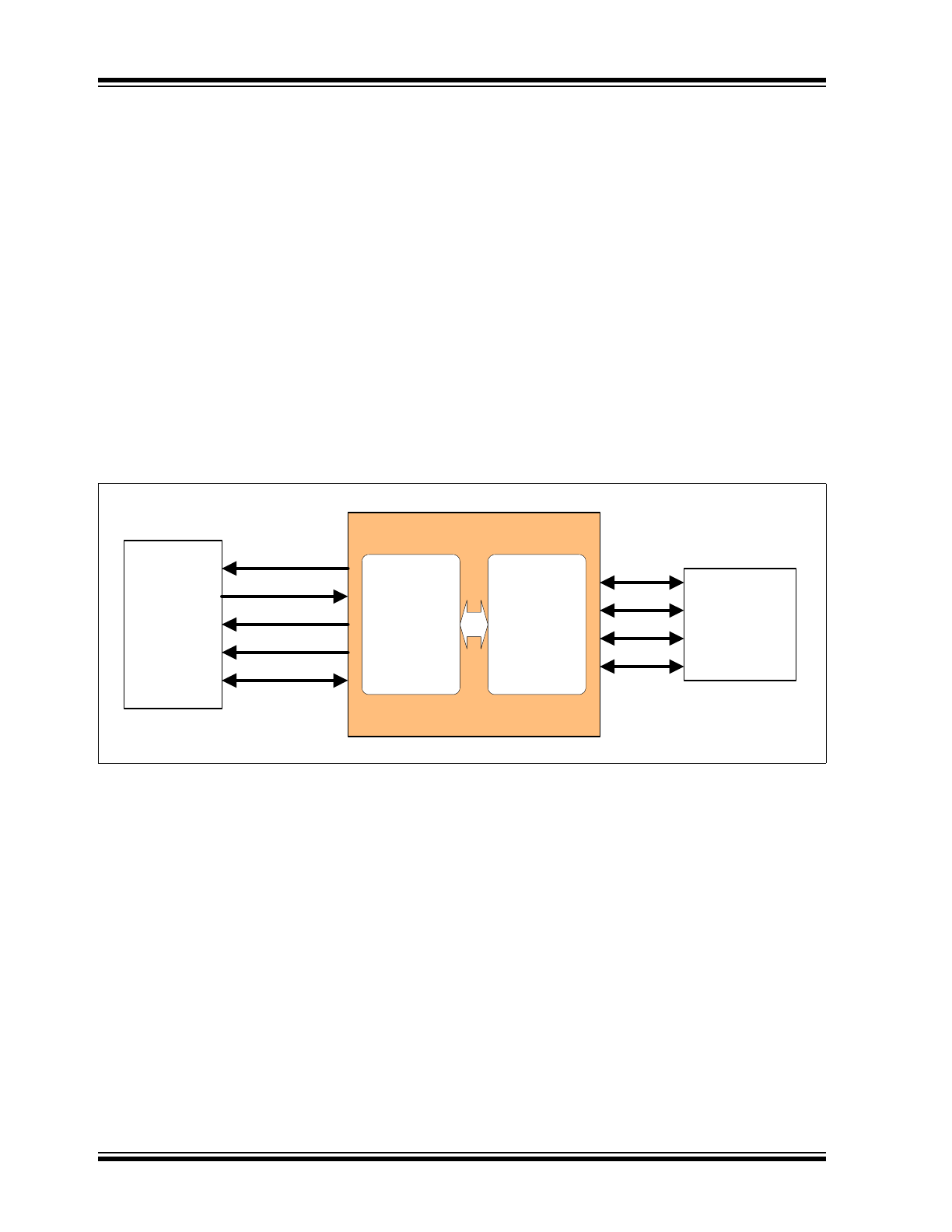
FIGURE 1-1:
BASIC ULPI USB DEVICE BLOCK DIAGRAM
USB3300
Hi-Speed
Analog
w/ OTG
ULPI
Digital
Logic
USB
Connector
(Standard
or Mini)
ULPI
LINK
DM
V
BUS
DP
ID
STP
CLK
DIR
NXT
DATA[7:0]
32 Pin QFN
2014-2015 Microchip Technology Inc.
DS00001783C-page 5
USB3300
1.2
Reference Documents
• Universal Serial Bus Specification, Revision 2.0, April 27, 2000
• On-The-Go Supplement to the USB 2.0 Specification, Revision 1.0a, June 24, 2003
• USB 2.0 Transceiver Macrocell Interface (UTMI) Specification, Version 1.02, May 27, 2000
• UTMI+ Specification, Revision 1.0, February 2, 2004
• UTMI+ Low Pin Interface (ULPI) Specification, Revision 1.1
FIGURE 1-2:
ULPI INTERFACE FEATURES AS RELATED TO UTMI+
UTMI+ Level 0
Hi-Speed Peripherals Only
A
D
DE
D FEA
T
URE
S
USB3300
ULPI
Hi-Speed Peripheral, host controllers, On-the-
Go devices with 12 pin interface
(HS, FS, LS, preamble packet)
UTMI+ Level 3
Hi-Speed Peripheral, host controllers, On-
the-Go devices
(HS, FS, LS, preamble packet)
UTMI+ Level 2
Hi-Speed Peripheral, host controllers, On-
the-Go devices
(HS, FS, and LS but no preamble packet)
UTMI+ Level 1
Hi-Speed Peripheral, host controllers,
and On-the-Go devices
(HS and FS Only)
USB3500
USB3450
USB3280
USB3250
USB3300
DS00001783C-page 6
2014-2015 Microchip Technology Inc.
2.0
FUNCTIONAL OVERVIEW
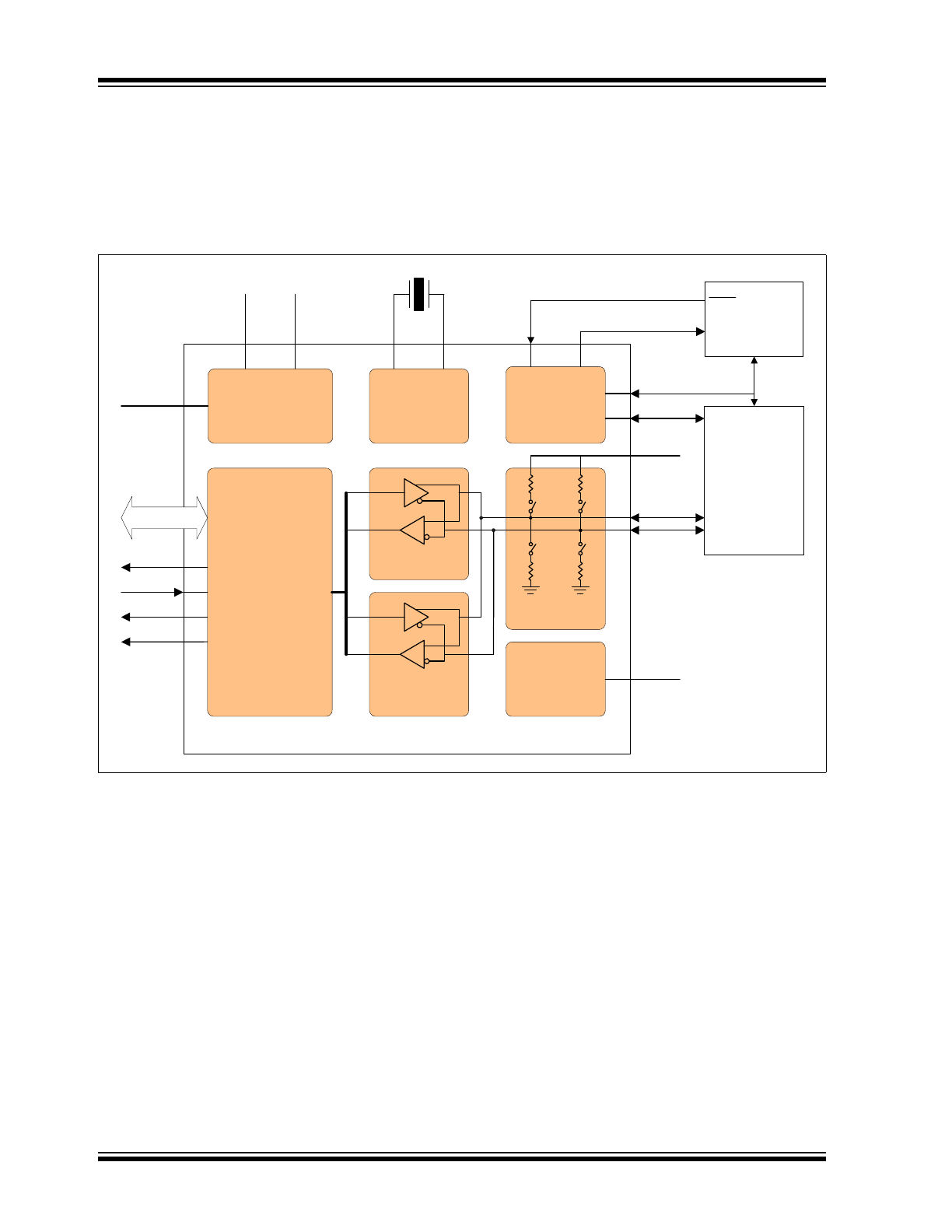
The USB3300 is a highly integrated USB PHY. It contains a complete Hi-Speed USB 2.0 PHY with the ULPI industry
standard interface to support fast time to market for a USB product. The USB3300 is composed of the functional blocks
shown in
Figure 2-1
below. Details of these individual blocks are described in
Architecture Overview on page 16
.
FIGURE 2-1:
USB3300 BLOCK DIAGRAM
ULPI Digital
OTG
Module
DATA[7:0]
24 MHz
XTAL
Internal
Regulator &
POR
5V
Power
Supply
Bias
Gen.
CLKOUT
NXT
DIR
STP
VDD3.3
XTAL &
PLL
XI
CPEN
VBUS
ID
VDD3.3
DP
DM
USB3300
VDD
1
.8
VDDA
1.8
m
XO
RBIAS
EXTVBUS
FAULT
Mini-AB
USB
Connector
HS XCVR
FS/LS
XCVR
Resistors
Rpu
_d
p
R
pd_
dm
Rp
d_
d
p
Rp
u_
dm
EN
2014-2015 Microchip Technology Inc.
DS00001783C-page 7
USB3300
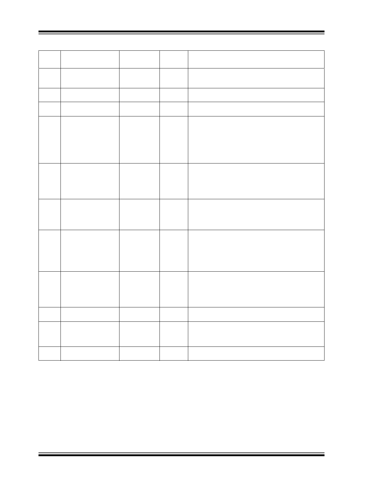
3.0
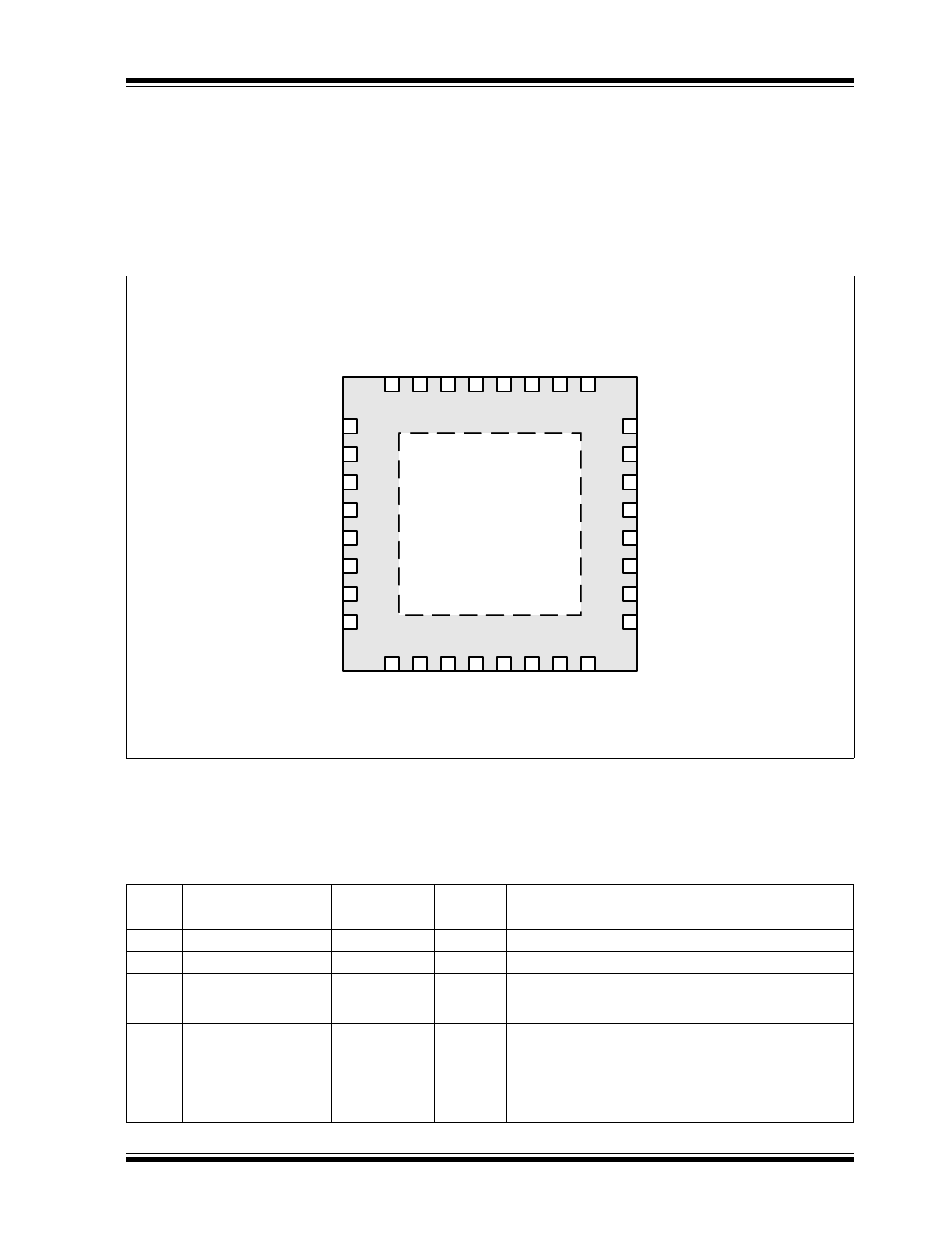
PIN LAYOUT
The USB3300 is offered in a 32 pin QFN package (5 x 5 x 0.9mm). The pin definitions and locations are documented
below.
3.1
USB3300 Pin Diagram
The exposed flag of the QFN package must be connected to ground with a via array to the ground plane. This is the
main ground connection for the USB3300.
3.2
Pin Function
FIGURE 3-1:
USB3300 PIN DIAGRAM - TOP VIEW
TABLE 3-1:
USB3300 PIN DEFINITIONS 32-PIN QFN PACKAGE
Pin
Name
Direction,
Type
Active
Level
Description
1
GND
Ground
N/A
Ground
2
GND
Ground
N/A
Ground
3
CPEN
Output,
CMOS
High
External 5 volt supply enable. This pin is used to
enable the external Vbus power supply. The CPEN pin
is low on POR.
4
VBUS
I/O,
Analog
N/A
VBUS pin of the USB cable. The USB3300 uses this
pin for the Vbus comparator inputs and for Vbus
pulsing during session request protocol.
5
ID
Input,
Analog
N/A
ID pin of the USB cable. For non-OTG applications
this pin can be floated. For an A-Device ID = 0. For a
B-Device ID = 1.
GND
GND
CPEN
VBUS
ID
VDD3.3
DM
DP
RE
SE
T
EX
T
V
B
U
S
NXT
DI
R
ST
P
CL
KOU
T
VDD3
.3
VDD1
.8
DATA0
DATA7
DATA5
DATA6
DATA2
DATA3
DATA4
DATA1
RB
IAS
VDD3
.3
XO
VDD1
.8
VDD3
.3
VDDA
1
.8
XI
RE
G_
EN
USB3300
Hi-Speed USB2
ULPI PHY
32 Pin QFN
1
2
3
4
5
6
7
8
USB3300
Hi-Speed USB
ULPI PHY
32 Pin QFN
GND FLAG
9
10
11
12
13
14
15
16
24
23
22
21
20
19
18
17
32
31
30
29
28
27
26
25
USB3300
DS00001783C-page 8
2014-2015 Microchip Technology Inc.
6
VDD3.3
Power
N/A
3.3V Supply. A 0.1uF bypass capacitor should be
connected between this pin and the ground plane on
the PCB.
7
DP
I/O,
Analog
N/A
D+ pin of the USB cable.
8
DM
I/O,
Analog
N/A
D- pin of the USB cable.
9
RESET
Input, CMOS
High
Optional active high transceiver reset. This is the
same as a write to the ULPI Reset, address 04h, bit
5. This does not reset the ULPI register set. This pin
includes an integrated pull-down resistor to ground. If
not used, this pin can be floated or connected to
ground (recommended).
See
Section 6.1.11, "Reset Pin"
for details.
10
EXTVBUS
Input, CMOS
High
External Vbus Detect. Connect to fault output of an
external USB power switch or an external Vbus Valid
comparator. See
Section 6.5.4, "External Vbus
Indicator," on page 38
for details. This pin has a pull
down resistor to prevent it from floating when the ULPI
bit UseExternalVbusIndicator is set to 0.
11
NXT
Output,
CMOS
High
The PHY asserts NXT to throttle the data. When the
Link is sending data to the PHY, NXT indicates when
the current byte has been accepted by the PHY. The
Link places the next byte on the data bus in the
following clock cycle.
12
DIR
Output,
CMOS
N/A
Controls the direction of the data bus. When the PHY
has data to transfer to the Link, it drives DIR high to
take ownership of the bus. When the PHY has no data
to transfer it drives DIR low and monitors the bus for
commands from the Link. The PHY will pull DIR high
whenever the interface cannot accept data from the
Link, such as during PLL start-up.
13
STP
Input,
CMOS
High
The Link asserts STP for one clock cycle to stop the
data stream currently on the bus. If the Link is sending
data to the PHY, STP indicates the last byte of data
was on the bus in the previous cycle. The STP pin
also includes the interface protection detailed in
Section 6.1.9.3, "Interface Protection," on page 31
.
14
CLKOUT
Output,
CMOS
N/A
60MHz reference clock output. All ULPI signals are
driven synchronous to the rising edge of this clock.
15
VDD1.8
Power
N/A
1.8V for digital circuitry on chip. Supplied by On-Chip
Regulator when REG_EN is active. Place a 0.1uF
capacitor near this pin and connect the capacitor from
this pin to ground. Connect pin 15 to pin 26.
16
VDD3.3
Power
N/A
A 0.1uF bypass capacitor should be connected
between this pin and the ground plane on the PCB.
TABLE 3-1:
USB3300 PIN DEFINITIONS 32-PIN QFN PACKAGE (CONTINUED)
Pin
Name
Direction,
Type
Active
Level
Description
2014-2015 Microchip Technology Inc.
DS00001783C-page 9
USB3300
17
DATA[7]
I/O,
CMOS,
Pull-low
N/A
8-bit bi-directional data bus. Bus ownership is
determined by DIR. The Link and PHY initiate data
transfers by driving a non-zero pattern onto the data
bus. ULPI defines interface timing for a single-edge
data transfers with respect to rising edge of CLKOUT.
DATA[7] is the MSB and DATA[0] is the LSB.
18
DATA[6]
I/O,
CMOS,
Pull-low
N/A
19
DATA[5]
I/O,
CMOS,
Pull-low
N/A
20
DATA[4]
I/O,
CMOS,
Pull-low
N/A
21
DATA[3]
I/O,
CMOS,
Pull-low
N/A
22
DATA[2]
I/O,
CMOS,
Pull-low
N/A
23
DATA[1]
I/O,
CMOS,
Pull-low
N/A
24
DATA[0]
I/O,
CMOS,
Pull-low
N/A
25
VDD3.3
Power
N/A
A 0.1uF bypass capacitor should be connected
between this pin and the ground plane on the PCB.
26
VDD1.8
Power
N/A
1.8V for digital circuitry on chip. Supplied by On-Chip
Regulator when REG_EN is active. When using the
internal regulators, place a 4.7uF low-ESR capacitor
near this pin and connect the capacitor from this pin
to ground. Connect pin 26 to pin 15. Do not connect
VDD1.8 to VDDA1.8 when using internal regulators.
When the regulators are disabled, pin 29 may be
connected to pins 26 and 15.
27
XO
Output,
Analog
N/A
Crystal pin. If using an external clock on XI this pin
should be floated.
28
XI
Input,
Analog
N/A
Crystal pin. A 24MHz crystal is supported. The crystal
is placed across XI and XO. An external 24MHz clock
source may be driven into XI in place of a crystal.
29
VDDA1.8
Power
N/A
1.8V for analog circuitry on chip. Supplied by On-Chip
Regulator when REG_EN is active. Place a 0.1uF
capacitor near this pin and connect the capacitor from
this pin to ground. When using the internal regulators,
place a 4.7uF low-ESR capacitor near this pin in
parallel with the 0.1uF capacitor. Do not connect
VDD1.8A to VDD1.8 when using internal regulators.
When the regulators are disabled, pin 29 may be
connected to pins 26 and 15.
30
VDD3.3
Power
N/A
Analog 3.3 volt supply. A 0.1uF low ESR bypass
capacitor connected to the ground plane of the PCB is
recommended.
TABLE 3-1:
USB3300 PIN DEFINITIONS 32-PIN QFN PACKAGE (CONTINUED)
Pin
Name
Direction,
Type
Active
Level
Description
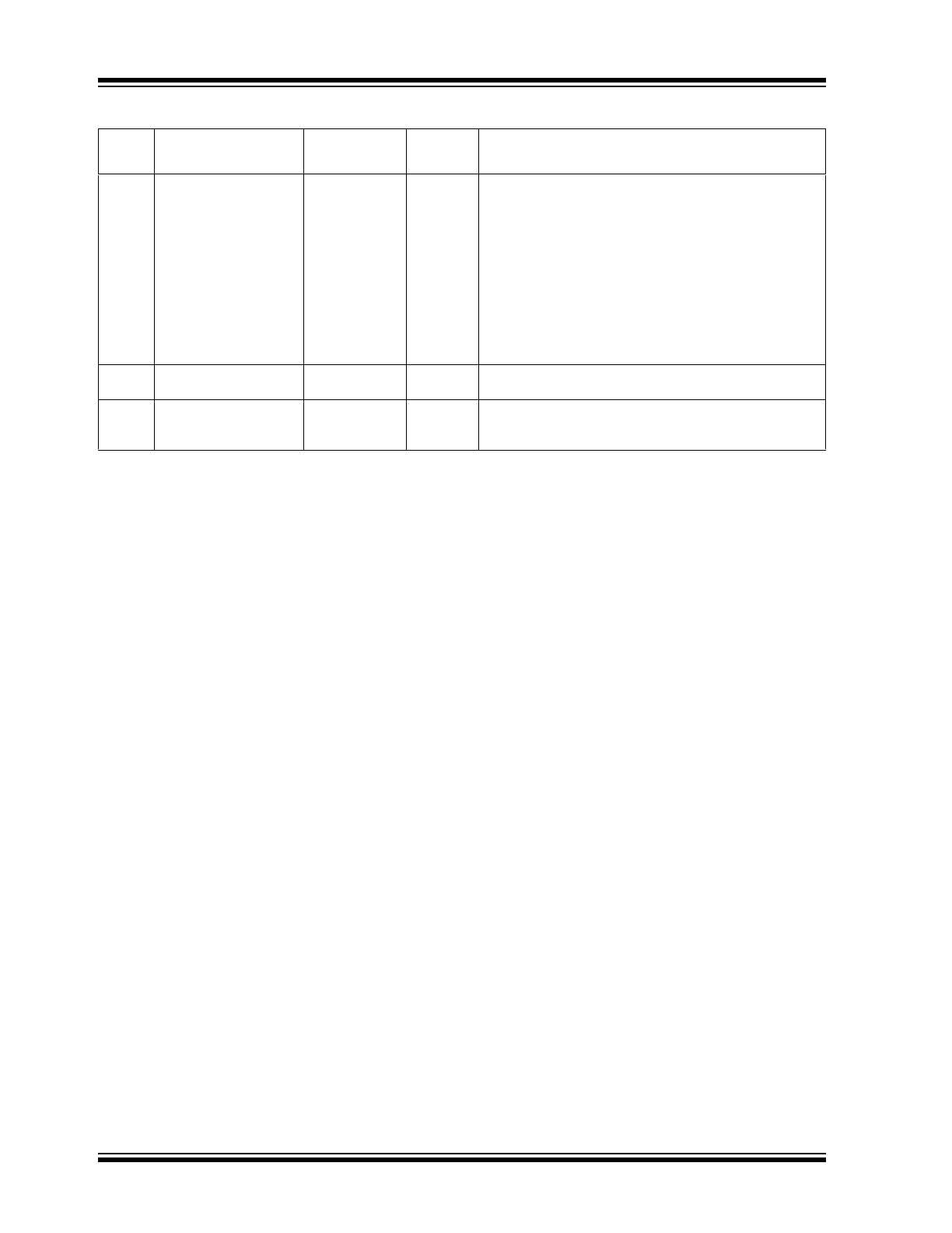
USB3300
DS00001783C-page 10
2014-2015 Microchip Technology Inc.
31
REG_EN
I/O,
CMOS,
Pull-low
N/A
On-Chip 1.8V regulator enable. Connect to ground to
disable both of the on chip (VDDA1.8 and VDD1.8)
regulators. When regulators are disabled:
• External 1.8V must be supplied to VDDA1.8 and
VDD1.8 pins. When the regulators are disabled,
VDDA1.8 may be connected to VDD1.8 and a
bypass capacitor (0.1uF recommended) should be
connected to each pin.
• The voltage at VDD3.3 must be at least 2.64V (0.8
* 3.3V) before voltage is applied to VDDA1.8 and
VDD1.8.
32
RBIAS
Analog,
CMOS
N/A
External 12KΩ +/- 1% bias resistor to ground.
GND FLAG
Ground
N/A
Ground. The flag must be connected to the ground
plane with a via array under the exposed flag. This is
the main ground for the IC.
TABLE 3-1:
USB3300 PIN DEFINITIONS 32-PIN QFN PACKAGE (CONTINUED)
Pin
Name
Direction,
Type
Active
Level
Description