

2004 - 2015 Microchip Technology Inc.
DS00001899A-page 1
Highlights
• Available in a 40-ball RoHS compliant
(4 x 4 x 0.9mm) VFBGA package
• Interface compliant with the UTMI specification
(60MHz, 8-bit bidirectional interface)
• Only one required power supply (+3.3V)
• Supports 480Mbps Hi-Speed (HS) and 12Mbps
Full Speed (FS) serial data transmission rates
• Integrated 45
Ω and 1.5kΩ termination resistors
reduce external component count
• Internal short circuit protection of DP and DM
lines
• On-chip oscillator operates with low cost 24MHz
crystal
• Latch-up performance exceeds 150mA per EIA/
JESD 78, Class II
• ESD protection levels of 5kV HBM without exter-
nal protection devices
• SYNC and EOP generation on transmit packets
and detection on receive packets
• NRZI encoding and decoding
• Bit stuffing and unstuffing with error detection
• Supports the USB suspend state, HS detection,
HS Chirp, Reset and Resume
• Support for all test modes defined in the USB 2.0
specification
• 55mA Unconfigured Current (typical) - ideal for
bus powered applications.
• 83uA suspend current (typical) - ideal for battery
powered applications.
• Industrial Operating Temperature -40
o
C to +85
o
C
Applications
The USB3290 is the ideal companion to any ASIC, SoC
or FPGA solution designed with a UTMI Hi-Speed USB
device (peripheral) core.
The USB3290 is well suited for:
• Cell Phones
• MP3 Players
• Scanners
• External Hard Drives
• Digital Still and Video Cameras
• Portable Media Players
• Entertainment Devices
• Printers
USB3290
Small Footprint Hi-Speed USB 2.0 Device PHY
with UTMI Interface

USB3290
DS00001899A-page 2
2004 - 2015 Microchip Technology Inc.
TO OUR VALUED CUSTOMERS
It is our intention to provide our valued customers with the best documentation possible to ensure successful use of your Microchip
products. To this end, we will continue to improve our publications to better suit your needs. Our publications will be refined and
enhanced as new volumes and updates are introduced.
If you have any questions or comments regarding this publication, please contact the Marketing Communications Department via
E-mail at
docerrors@microchip.com
. We welcome your feedback.
Most Current Data Sheet
To obtain the most up-to-date version of this data sheet, please register at our Worldwide Web site at:
http://www.microchip.com
You can determine the version of a data sheet by examining its literature number found on the bottom outside corner of any page.
The last character of the literature number is the version number, (e.g., DS30000000A is version A of document DS30000000).
Errata
An errata sheet, describing minor operational differences from the data sheet and recommended workarounds, may exist for cur-
rent devices. As device/documentation issues become known to us, we will publish an errata sheet. The errata will specify the
revision of silicon and revision of document to which it applies.
To determine if an errata sheet exists for a particular device, please check with one of the following:
• Microchip’s Worldwide Web site;
http://www.microchip.com
• Your local Microchip sales office (see last page)
When contacting a sales office, please specify which device, revision of silicon and data sheet (include -literature number) you are
using.
Customer Notification System
Register on our web site at
www.microchip.com
to receive the most current information on all of our products.

2004 - 2015 Microchip Technology Inc.
DS00001899A-page 3
USB3290
Table of Contents
1.0 Introduction ..................................................................................................................................................................................... 4
2.0 Functional Block Diagram ............................................................................................................................................................... 5
3.0 Pin Layout ....................................................................................................................................................................................... 6
4.0 Interface Signal Definition ............................................................................................................................................................... 7
5.0 Limiting Values .............................................................................................................................................................................. 10
6.0 Electrical Characteristics ............................................................................................................................................................... 11
7.0 Functional Overview ..................................................................................................................................................................... 17
8.0 Application Notes .......................................................................................................................................................................... 24
9.0 Package Outline ............................................................................................................................................................................ 38
Appendix A: Data Sheet Revision History ........................................................................................................................................... 42
The Microchip Web Site ...................................................................................................................................................................... 43
Customer Change Notification Service ............................................................................................................................................... 43
Customer Support ............................................................................................................................................................................... 43
Product Identification System ............................................................................................................................................................. 44

USB3290
DS00001899A-page 4
2004 - 2015 Microchip Technology Inc.
1.0
INTRODUCTION
The USB3290 provides the Physical Layer (PHY) interface to a USB 2.0 Device Controller. The IC is available in a 40-
ball RoHS compliant VFBGA package. The small footprint package makes the USB3290 ideal for portable consumer
electronics applications.
1.1
Product Description
The USB3290 is an industrial temperature USB 2.0 physical layer transceiver (PHY) integrated circuit. Microchip’s pro-
prietary technology results in low power dissipation, which is ideal for building a bus powered USB 2.0 peripheral. The
PHY uses an 8-bit bidirectional parallel interface, which complies with the USB Transceiver Macrocell Interface (UTMI)
specification. It supports 480Mbps transfer rate, while remaining backward compatible with USB 1.1 legacy protocol at
12Mbps.
All required termination and 5.25V short circuit protection of the DP/DM lines are internal to the chip. The USB3290 also
has an integrated 1.8V regulator so that only a 3.3V supply is required.
While transmitting data, the PHY serializes data and generates SYNC and EOP fields. It also performs needed bit stuff-
ing and NRZI encoding. Likewise, while receiving data, the PHY de-serializes incoming data, stripping SYNC and EOP
fields and performs bit un-stuffing and NRZI decoding.
2004 - 2015 Microchip Technology Inc.
DS00001899A-page 5
USB3290
2.0
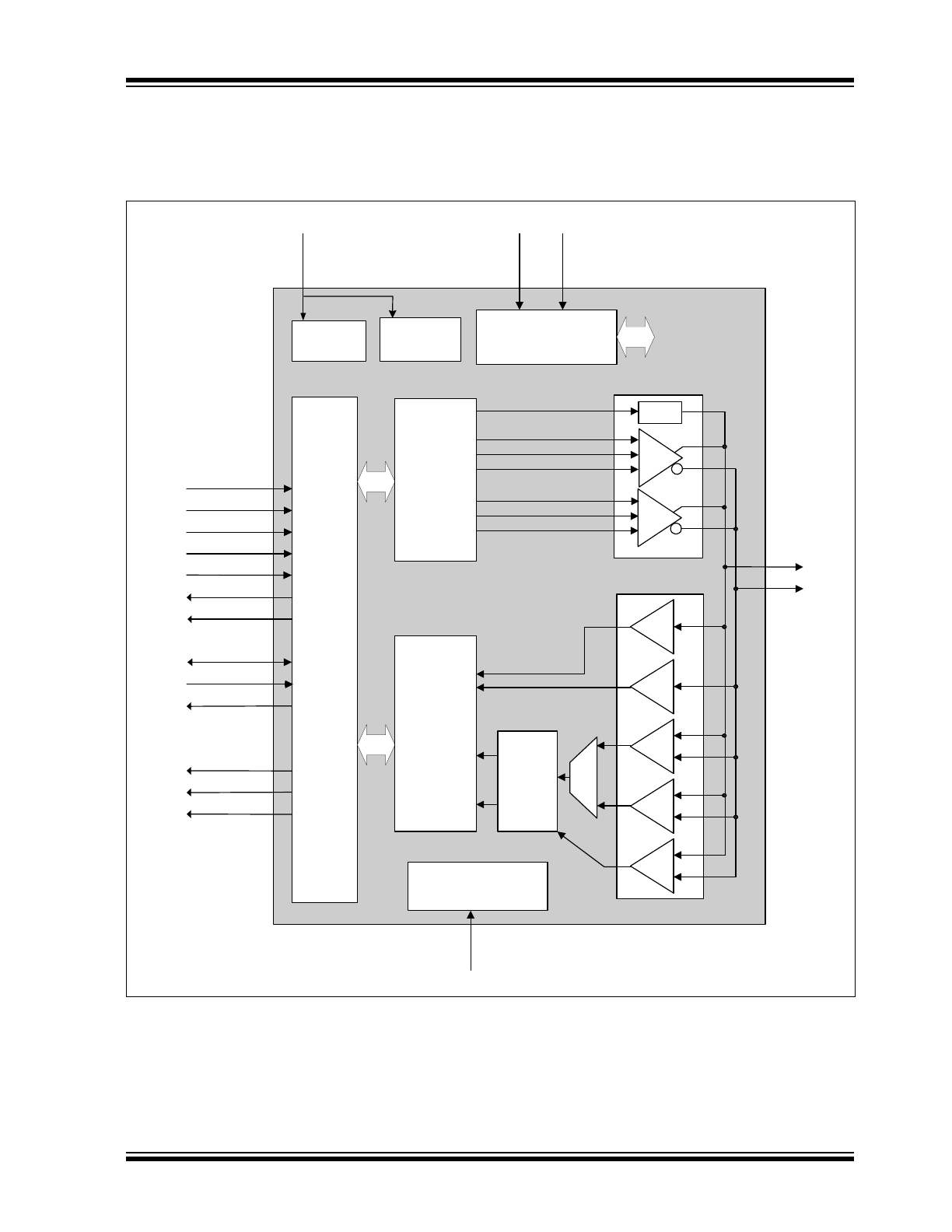
FUNCTIONAL BLOCK DIAGRAM
FIGURE 2-1:
USB3290 BLOCK DIAGRAM
PWR
Control
FS SE+
R
X
UTMI
In
te
r
fac
e
TX State
Machine
Parallel to
Serial
Conversion
Bit Stuff
NRZI
Encode
TX
LOGIC
Clock
Recovery Unit
Clock
and
Data
Recovery
Elasticity
Buffer
VP
VM
BIASING
Bandgap Voltage Reference
Current Reference
RB
IA
S
VD
D3
.3
PLL and
XTAL OSC
System
Clocking
FS RX
FS SE-
HS RX
HS SQ
RX State
Machine
Serial to
Parallel
Conversion
Bit Unstuff
NRZI
Decode
RX
LOGIC
DM
TX
1.5k
Ω
FS
TX
HS
TX
HS_DATA
HS_CS_ENABLE
HS_DRIVE_ENABLE
OEB
VMO
VPO
RPU_EN
MU
X
DP
RXVALID
RXACTIVE
RXERROR
TXREADY
RESET
SUSPENDN
XCVRSELECT
TERMSELECT
OPMODE[1:0]
LINESTATE[1:0]
CLKOUT
TXVALID
DATA[7:0]
XI
XO
1.8V
Regulator
USB3290
DS00001899A-page 6
2004 - 2015 Microchip Technology Inc.
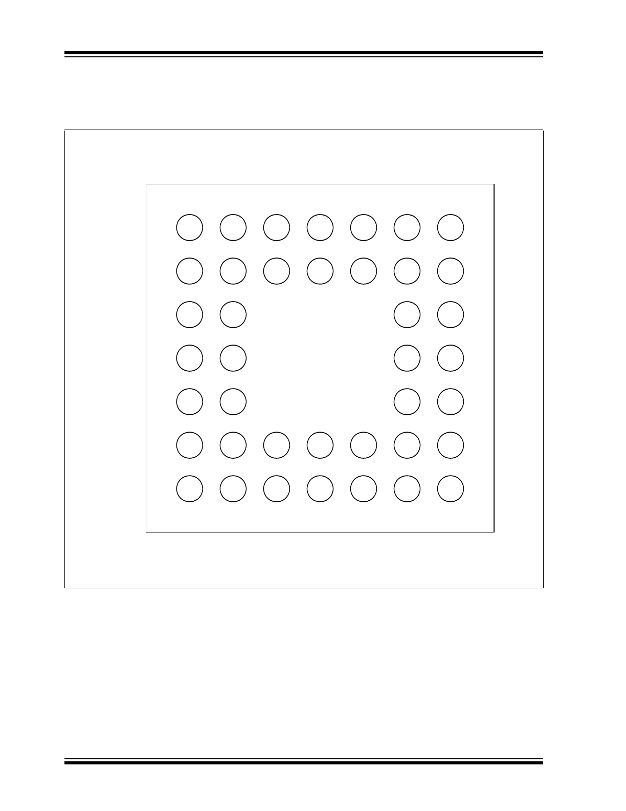
3.0
PIN LAYOUT
FIGURE 3-1:
USB3290 PIN LAYOUT - TOP VIEW
TOP VIEW
TSEL
TXR
SPDN
TXV
RST
V33
V33
DP
XSEL
GND
CLK
DM
V33
RXA
OM0
LS1
LS0
OM1
D6
D7
RXV
D0
D5
D2
D3
D4
D1
RB
VIO
V18A
XI
XO
V18
V33
RXE
REN
G
E
C
B
A
F
D
1
7
6
5
4
3
2
GND
GND
GND
VIO
2004 - 2015 Microchip Technology Inc.
DS00001899A-page 7
USB3290
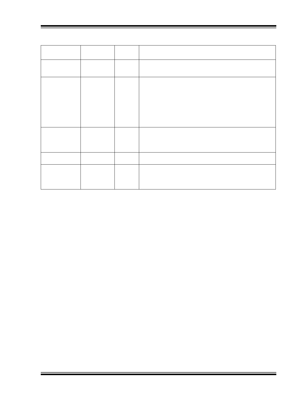
4.0
INTERFACE SIGNAL DEFINITION
TABLE 4-1:
SYSTEM INTERFACE SIGNALS
Name
Direction
Active
Level
Description
RESET
(RST)
Input
High
Reset.
Reset all state machines. After coming out of reset,
must wait 5 rising edges of clock before asserting TXValid
for transmit.
See
Section 7.8.3
XCVRSELECT
(XSEL)
Input
N/A
Transceiver Select.
This signal selects between the FS
and HS transceivers:
0: HS transceiver enabled
1: FS transceiver enabled.
TERMSELECT
(TSEL)
Input
N/A
Termination Select.
This signal selects between the FS
and HS terminations:
0: HS termination enabled
1: FS termination enabled
SUSPENDN
(SPDN)
Input
Low
Suspend.
Places the transceiver in a mode that draws
minimal power from supplies. Shuts down all blocks not
necessary for Suspend/Resume operation. While
suspended, TERMSELECT must always be in FS mode to
ensure that the 1.5k
Ω pull-up on DP remains powered.
0: Transceiver circuitry drawing suspend current
1: Transceiver circuitry drawing normal current
CLKOUT
(CLK)
Output
Rising Edge
System Clock
. This output is used for clocking receive
and transmit parallel data at 60MHz.
OPMODE[1:0]
(OM1)
(OM0)
Input
N/A
Operational Mode.
These signals select between the
various operational modes:
[1] [0] Description
0 0 0: Normal Operation
0 1 1: Non-driving (all terminations removed)
1 0 2: Disable bit stuffing and NRZI encoding
1 1 3: Reserved
LINESTATE[1:0]
(LS1)
(LS0)
Output
N/A
Line State
. These signals reflect the current state of the
USB data bus in FS mode, with [0] reflecting the state of
DP and [1] reflecting the state of DM. When the device is
suspended or resuming from a suspended state, the
signals are combinatorial. Otherwise, the signals are
synchronized to CLKOUT.
[1] [0] Description
0 0 0: SE0
0 1 1: J State
1 0 2: K State
1 1 3: SE1
USB3290
DS00001899A-page 8
2004 - 2015 Microchip Technology Inc.
TABLE 4-2:
DATA INTERFACE SIGNALS
Name
Direction
Active
Level
Description
DATA[7:0]
(D7)
.
.
.
(D0)
Bidirectional
High
Data bus. 8-bit Bidirectional mode.
TXVALID
DATA[7:0]
0
output
1
input
TXVALID
(TXV)
Input
High
Transmit Valid.
Indicates that the DATA bus is valid for transmit. The
assertion of TXVALID initiates the transmission of SYNC on the USB
bus. The negation of TXVALID initiates EOP on the USB.
Control inputs (OPMODE[1:0], TERMSELECT,XCVRSELECT) must not
be changed on the de-assertion or assertion of TXVALID. The PHY
must be in a quiescent state when these inputs are changed.
TXREADY
(TXR)
Output
High
Transmit Data Ready.
If TXVALID is asserted, the SIE must always
have data available for clocking into the TX Holding Register on the
rising edge of CLKOUT. TXREADY is an acknowledgement to the SIE
that the transceiver has clocked the data from the bus and is ready for
the next transfer on the bus. If TXVALID is negated, TXREADY can
be ignored by the SIE.
RXVALID
(RXV)
Output
High
Receive Data Valid.
Indicates that the DATA bus has received valid
data. The Receive Data Holding Register is full and ready to be
unloaded. The SIE is expected to latch the DATA bus on the rising edge
of CLKOUT.
RXACTIVE
(RXA)
Output
High
Receive Active.
Indicates that the receive state machine has detected
Start of Packet and is active.
RXERROR
(RXE)
Output
High
Receive Error
.
0: Indicates no error.
1: Indicates a receive error has been detected.
This output is clocked with the same timing as the receive DATA lines
and can occur at anytime during a transfer.
TABLE 4-3:
USB I/O SIGNALS
Name
Direction
Active
Level
Description
DP
I/O
N/A
USB Positive Data Pin.
DM
I/O
N/A
USB Negative Data Pin.
TABLE 4-4:
BIASING AND CLOCK OSCILLATOR SIGNALS
Name
Direction
Active
Level
Description
RBIAS
(RB)
Input
N/A
External 1% bias resistor.
Requires a 12kΩ resistor to ground.
Used for setting HS transmit current level and on-chip termination
impedance.
XI/XO
Input
N/A
External crystal.
24MHz crystal connected from XI to XO.
2004 - 2015 Microchip Technology Inc.
DS00001899A-page 9
USB3290
TABLE 4-5:
POWER AND GROUND SIGNALS
Name
Direction
Active
Level
Description
VDD3.3
(V33)
(VIO)
N/A
N/A
3.3V Supply.
Provides power for USB 2.0 Transceiver, UTMI+
Digital, Digital I/O, and Regulators.
REG_EN
(REN)
Input
High
On-Chip 1.8V regulator enable.
Connect to ground to disable
both of the on chip (VDDA1.8 and VDD1.8) regulators. When
regulators are disabled:
• External 1.8V must be supplied to VDDA1.8 and VDD1.8 pins.
When the regulators are disabled, VDDA1.8 may be con-
nected to VDD1.8 and a bypass capacitor (0.1
μF recom-
mended) should be connected to each pin.
• The voltage at VDD3.3 must be at least 2.64V (0.8 * 3.3V)
before voltage is applied to VDDA1.8 and VDD1.8.
VDD1.8
(V18)
N/A
N/A
1.8V Digital Supply.
Supplied by On-Chip Regulator when
REG_EN is active. Low ESR 4.7uF minimum capacitor
requirement when using internal regulators. Do not connect
VDD1.8 to VDDA1.8 when using internal regulators. When the
regulators are disabled, VDD1.8 may be connected to VDD1.8A.
VSS
(GND)
N/A
N/A
Common Ground.
VDDA1.8
(V18A)
N/A
N/A
1.8V Analog Supply.
Supplied by On-Chip Regulator when
REG_EN is active. Low ESR 4.7uF minimum capacitor
requirement when using internal regulators. Do not connect
VDD1.8A to VDD1.8 when using internal regulators. When the
regulators are disabled, VDD1.8A may be connected to VDD1.8.
USB3290
DS00001899A-page 10
2004 - 2015 Microchip Technology Inc.
5.0
LIMITING VALUES
TABLE 5-1:
ABSOLUTE MAXIMUM RATINGS
Parameter
Symbol
Conditions
MIN
TYP MAX
Units
Maximum DP and DM
voltage to Ground
V
MAX_5V
-0.3
5.5
V
Maximum VDD1.8 and
VDDA1.8 voltage to Ground
V
MAX_1.8V
-0.3
2.5
V
Maximum 3.3V Supply
Voltage to Ground
V
MAX_3.3V
-0.3
4.0
V
Maximum I/O Voltage to
Ground
V
I
-0.3
4.0
V
Storage Temperature
T
STG
-55
150
o
C
ESD PERFORMANCE
All Pins
V
HBM
Human Body Model
±5 kV
LATCH-UP PERFORMANCE
All Pins
I
LTCH_UP
EIA/JESD 78, Class II
150
mA
Note:
In accordance with the Absolute Maximum Rating system (IEC 60134).
TABLE 5-2:
RECOMMENDED OPERATING CONDITIONS
Parameter
Symbol
Conditions
MIN
TYP MAX
Units
3.3V Supply Voltage
(VDD3.3 and VDDA3.3)
V
DD3.3
3.0
3.3
3.6
V
Input Voltage on Digital Pins V
I
0.0
V
DD3.3
V
Input Voltage on Analog I/O
Pins (DP, DM)
V
I(I/O)
0.0
V
DD3.3
V
Ambient Temperature
T
A
-40
85
o
C
TABLE 5-3:
RECOMMENDED EXTERNAL CLOCK CONDITIONS
Parameter
Symbol
Conditions
MIN
TYP MAX
Units
System Clock Frequency
XO driven by the external clock;
and no connection at XI
24
(±100ppm)
MHz
System Clock Duty Cycle
XO driven by the external clock;
and no connection at XI
45
50
55
%
2004 - 2015 Microchip Technology Inc.
DS00001899A-page 1
Highlights
• Available in a 40-ball RoHS compliant
(4 x 4 x 0.9mm) VFBGA package
• Interface compliant with the UTMI specification
(60MHz, 8-bit bidirectional interface)
• Only one required power supply (+3.3V)
• Supports 480Mbps Hi-Speed (HS) and 12Mbps
Full Speed (FS) serial data transmission rates
• Integrated 45
Ω and 1.5kΩ termination resistors
reduce external component count
• Internal short circuit protection of DP and DM
lines
• On-chip oscillator operates with low cost 24MHz
crystal
• Latch-up performance exceeds 150mA per EIA/
JESD 78, Class II
• ESD protection levels of 5kV HBM without exter-
nal protection devices
• SYNC and EOP generation on transmit packets
and detection on receive packets
• NRZI encoding and decoding
• Bit stuffing and unstuffing with error detection
• Supports the USB suspend state, HS detection,
HS Chirp, Reset and Resume
• Support for all test modes defined in the USB 2.0
specification
• 55mA Unconfigured Current (typical) - ideal for
bus powered applications.
• 83uA suspend current (typical) - ideal for battery
powered applications.
• Industrial Operating Temperature -40
o
C to +85
o
C
Applications
The USB3290 is the ideal companion to any ASIC, SoC
or FPGA solution designed with a UTMI Hi-Speed USB
device (peripheral) core.
The USB3290 is well suited for:
• Cell Phones
• MP3 Players
• Scanners
• External Hard Drives
• Digital Still and Video Cameras
• Portable Media Players
• Entertainment Devices
• Printers
USB3290
Small Footprint Hi-Speed USB 2.0 Device PHY
with UTMI Interface
USB3290
DS00001899A-page 2
2004 - 2015 Microchip Technology Inc.
TO OUR VALUED CUSTOMERS
It is our intention to provide our valued customers with the best documentation possible to ensure successful use of your Microchip
products. To this end, we will continue to improve our publications to better suit your needs. Our publications will be refined and
enhanced as new volumes and updates are introduced.
If you have any questions or comments regarding this publication, please contact the Marketing Communications Department via
E-mail at
docerrors@microchip.com
. We welcome your feedback.
Most Current Data Sheet
To obtain the most up-to-date version of this data sheet, please register at our Worldwide Web site at:
http://www.microchip.com
You can determine the version of a data sheet by examining its literature number found on the bottom outside corner of any page.
The last character of the literature number is the version number, (e.g., DS30000000A is version A of document DS30000000).
Errata
An errata sheet, describing minor operational differences from the data sheet and recommended workarounds, may exist for cur-
rent devices. As device/documentation issues become known to us, we will publish an errata sheet. The errata will specify the
revision of silicon and revision of document to which it applies.
To determine if an errata sheet exists for a particular device, please check with one of the following:
• Microchip’s Worldwide Web site;
http://www.microchip.com
• Your local Microchip sales office (see last page)
When contacting a sales office, please specify which device, revision of silicon and data sheet (include -literature number) you are
using.
Customer Notification System
Register on our web site at
www.microchip.com
to receive the most current information on all of our products.
2004 - 2015 Microchip Technology Inc.
DS00001899A-page 3
USB3290
Table of Contents
1.0 Introduction ..................................................................................................................................................................................... 4
2.0 Functional Block Diagram ............................................................................................................................................................... 5
3.0 Pin Layout ....................................................................................................................................................................................... 6
4.0 Interface Signal Definition ............................................................................................................................................................... 7
5.0 Limiting Values .............................................................................................................................................................................. 10
6.0 Electrical Characteristics ............................................................................................................................................................... 11
7.0 Functional Overview ..................................................................................................................................................................... 17
8.0 Application Notes .......................................................................................................................................................................... 24
9.0 Package Outline ............................................................................................................................................................................ 38
Appendix A: Data Sheet Revision History ........................................................................................................................................... 42
The Microchip Web Site ...................................................................................................................................................................... 43
Customer Change Notification Service ............................................................................................................................................... 43
Customer Support ............................................................................................................................................................................... 43
Product Identification System ............................................................................................................................................................. 44
USB3290
DS00001899A-page 4
2004 - 2015 Microchip Technology Inc.
1.0
INTRODUCTION
The USB3290 provides the Physical Layer (PHY) interface to a USB 2.0 Device Controller. The IC is available in a 40-
ball RoHS compliant VFBGA package. The small footprint package makes the USB3290 ideal for portable consumer
electronics applications.
1.1
Product Description
The USB3290 is an industrial temperature USB 2.0 physical layer transceiver (PHY) integrated circuit. Microchip’s pro-
prietary technology results in low power dissipation, which is ideal for building a bus powered USB 2.0 peripheral. The
PHY uses an 8-bit bidirectional parallel interface, which complies with the USB Transceiver Macrocell Interface (UTMI)
specification. It supports 480Mbps transfer rate, while remaining backward compatible with USB 1.1 legacy protocol at
12Mbps.
All required termination and 5.25V short circuit protection of the DP/DM lines are internal to the chip. The USB3290 also
has an integrated 1.8V regulator so that only a 3.3V supply is required.
While transmitting data, the PHY serializes data and generates SYNC and EOP fields. It also performs needed bit stuff-
ing and NRZI encoding. Likewise, while receiving data, the PHY de-serializes incoming data, stripping SYNC and EOP
fields and performs bit un-stuffing and NRZI decoding.
2004 - 2015 Microchip Technology Inc.
DS00001899A-page 5
USB3290
2.0
FUNCTIONAL BLOCK DIAGRAM
FIGURE 2-1:
USB3290 BLOCK DIAGRAM
PWR
Control
FS SE+
R
X
UTMI
In
te
r
fac
e
TX State
Machine
Parallel to
Serial
Conversion
Bit Stuff
NRZI
Encode
TX
LOGIC
Clock
Recovery Unit
Clock
and
Data
Recovery
Elasticity
Buffer
VP
VM
BIASING
Bandgap Voltage Reference
Current Reference
RB
IA
S
VD
D3
.3
PLL and
XTAL OSC
System
Clocking
FS RX
FS SE-
HS RX
HS SQ
RX State
Machine
Serial to
Parallel
Conversion
Bit Unstuff
NRZI
Decode
RX
LOGIC
DM
TX
1.5k
Ω
FS
TX
HS
TX
HS_DATA
HS_CS_ENABLE
HS_DRIVE_ENABLE
OEB
VMO
VPO
RPU_EN
MU
X
DP
RXVALID
RXACTIVE
RXERROR
TXREADY
RESET
SUSPENDN
XCVRSELECT
TERMSELECT
OPMODE[1:0]
LINESTATE[1:0]
CLKOUT
TXVALID
DATA[7:0]
XI
XO
1.8V
Regulator
USB3290
DS00001899A-page 6
2004 - 2015 Microchip Technology Inc.
3.0
PIN LAYOUT
FIGURE 3-1:
USB3290 PIN LAYOUT - TOP VIEW
TOP VIEW
TSEL
TXR
SPDN
TXV
RST
V33
V33
DP
XSEL
GND
CLK
DM
V33
RXA
OM0
LS1
LS0
OM1
D6
D7
RXV
D0
D5
D2
D3
D4
D1
RB
VIO
V18A
XI
XO
V18
V33
RXE
REN
G
E
C
B
A
F
D
1
7
6
5
4
3
2
GND
GND
GND
VIO
2004 - 2015 Microchip Technology Inc.
DS00001899A-page 7
USB3290
4.0
INTERFACE SIGNAL DEFINITION
TABLE 4-1:
SYSTEM INTERFACE SIGNALS
Name
Direction
Active
Level
Description
RESET
(RST)
Input
High
Reset.
Reset all state machines. After coming out of reset,
must wait 5 rising edges of clock before asserting TXValid
for transmit.
See
Section 7.8.3
XCVRSELECT
(XSEL)
Input
N/A
Transceiver Select.
This signal selects between the FS
and HS transceivers:
0: HS transceiver enabled
1: FS transceiver enabled.
TERMSELECT
(TSEL)
Input
N/A
Termination Select.
This signal selects between the FS
and HS terminations:
0: HS termination enabled
1: FS termination enabled
SUSPENDN
(SPDN)
Input
Low
Suspend.
Places the transceiver in a mode that draws
minimal power from supplies. Shuts down all blocks not
necessary for Suspend/Resume operation. While
suspended, TERMSELECT must always be in FS mode to
ensure that the 1.5k
Ω pull-up on DP remains powered.
0: Transceiver circuitry drawing suspend current
1: Transceiver circuitry drawing normal current
CLKOUT
(CLK)
Output
Rising Edge
System Clock
. This output is used for clocking receive
and transmit parallel data at 60MHz.
OPMODE[1:0]
(OM1)
(OM0)
Input
N/A
Operational Mode.
These signals select between the
various operational modes:
[1] [0] Description
0 0 0: Normal Operation
0 1 1: Non-driving (all terminations removed)
1 0 2: Disable bit stuffing and NRZI encoding
1 1 3: Reserved
LINESTATE[1:0]
(LS1)
(LS0)
Output
N/A
Line State
. These signals reflect the current state of the
USB data bus in FS mode, with [0] reflecting the state of
DP and [1] reflecting the state of DM. When the device is
suspended or resuming from a suspended state, the
signals are combinatorial. Otherwise, the signals are
synchronized to CLKOUT.
[1] [0] Description
0 0 0: SE0
0 1 1: J State
1 0 2: K State
1 1 3: SE1
USB3290
DS00001899A-page 8
2004 - 2015 Microchip Technology Inc.
TABLE 4-2:
DATA INTERFACE SIGNALS
Name
Direction
Active
Level
Description
DATA[7:0]
(D7)
.
.
.
(D0)
Bidirectional
High
Data bus. 8-bit Bidirectional mode.
TXVALID
DATA[7:0]
0
output
1
input
TXVALID
(TXV)
Input
High
Transmit Valid.
Indicates that the DATA bus is valid for transmit. The
assertion of TXVALID initiates the transmission of SYNC on the USB
bus. The negation of TXVALID initiates EOP on the USB.
Control inputs (OPMODE[1:0], TERMSELECT,XCVRSELECT) must not
be changed on the de-assertion or assertion of TXVALID. The PHY
must be in a quiescent state when these inputs are changed.
TXREADY
(TXR)
Output
High
Transmit Data Ready.
If TXVALID is asserted, the SIE must always
have data available for clocking into the TX Holding Register on the
rising edge of CLKOUT. TXREADY is an acknowledgement to the SIE
that the transceiver has clocked the data from the bus and is ready for
the next transfer on the bus. If TXVALID is negated, TXREADY can
be ignored by the SIE.
RXVALID
(RXV)
Output
High
Receive Data Valid.
Indicates that the DATA bus has received valid
data. The Receive Data Holding Register is full and ready to be
unloaded. The SIE is expected to latch the DATA bus on the rising edge
of CLKOUT.
RXACTIVE
(RXA)
Output
High
Receive Active.
Indicates that the receive state machine has detected
Start of Packet and is active.
RXERROR
(RXE)
Output
High
Receive Error
.
0: Indicates no error.
1: Indicates a receive error has been detected.
This output is clocked with the same timing as the receive DATA lines
and can occur at anytime during a transfer.
TABLE 4-3:
USB I/O SIGNALS
Name
Direction
Active
Level
Description
DP
I/O
N/A
USB Positive Data Pin.
DM
I/O
N/A
USB Negative Data Pin.
TABLE 4-4:
BIASING AND CLOCK OSCILLATOR SIGNALS
Name
Direction
Active
Level
Description
RBIAS
(RB)
Input
N/A
External 1% bias resistor.
Requires a 12kΩ resistor to ground.
Used for setting HS transmit current level and on-chip termination
impedance.
XI/XO
Input
N/A
External crystal.
24MHz crystal connected from XI to XO.
2004 - 2015 Microchip Technology Inc.
DS00001899A-page 9
USB3290
TABLE 4-5:
POWER AND GROUND SIGNALS
Name
Direction
Active
Level
Description
VDD3.3
(V33)
(VIO)
N/A
N/A
3.3V Supply.
Provides power for USB 2.0 Transceiver, UTMI+
Digital, Digital I/O, and Regulators.
REG_EN
(REN)
Input
High
On-Chip 1.8V regulator enable.
Connect to ground to disable
both of the on chip (VDDA1.8 and VDD1.8) regulators. When
regulators are disabled:
• External 1.8V must be supplied to VDDA1.8 and VDD1.8 pins.
When the regulators are disabled, VDDA1.8 may be con-
nected to VDD1.8 and a bypass capacitor (0.1
μF recom-
mended) should be connected to each pin.
• The voltage at VDD3.3 must be at least 2.64V (0.8 * 3.3V)
before voltage is applied to VDDA1.8 and VDD1.8.
VDD1.8
(V18)
N/A
N/A
1.8V Digital Supply.
Supplied by On-Chip Regulator when
REG_EN is active. Low ESR 4.7uF minimum capacitor
requirement when using internal regulators. Do not connect
VDD1.8 to VDDA1.8 when using internal regulators. When the
regulators are disabled, VDD1.8 may be connected to VDD1.8A.
VSS
(GND)
N/A
N/A
Common Ground.
VDDA1.8
(V18A)
N/A
N/A
1.8V Analog Supply.
Supplied by On-Chip Regulator when
REG_EN is active. Low ESR 4.7uF minimum capacitor
requirement when using internal regulators. Do not connect
VDD1.8A to VDD1.8 when using internal regulators. When the
regulators are disabled, VDD1.8A may be connected to VDD1.8.
USB3290
DS00001899A-page 10
2004 - 2015 Microchip Technology Inc.
5.0
LIMITING VALUES
TABLE 5-1:
ABSOLUTE MAXIMUM RATINGS
Parameter
Symbol
Conditions
MIN
TYP MAX
Units
Maximum DP and DM
voltage to Ground
V
MAX_5V
-0.3
5.5
V
Maximum VDD1.8 and
VDDA1.8 voltage to Ground
V
MAX_1.8V
-0.3
2.5
V
Maximum 3.3V Supply
Voltage to Ground
V
MAX_3.3V
-0.3
4.0
V
Maximum I/O Voltage to
Ground
V
I
-0.3
4.0
V
Storage Temperature
T
STG
-55
150
o
C
ESD PERFORMANCE
All Pins
V
HBM
Human Body Model
±5 kV
LATCH-UP PERFORMANCE
All Pins
I
LTCH_UP
EIA/JESD 78, Class II
150
mA
Note:
In accordance with the Absolute Maximum Rating system (IEC 60134).
TABLE 5-2:
RECOMMENDED OPERATING CONDITIONS
Parameter
Symbol
Conditions
MIN
TYP MAX
Units
3.3V Supply Voltage
(VDD3.3 and VDDA3.3)
V
DD3.3
3.0
3.3
3.6
V
Input Voltage on Digital Pins V
I
0.0
V
DD3.3
V
Input Voltage on Analog I/O
Pins (DP, DM)
V
I(I/O)
0.0
V
DD3.3
V
Ambient Temperature
T
A
-40
85
o
C
TABLE 5-3:
RECOMMENDED EXTERNAL CLOCK CONDITIONS
Parameter
Symbol
Conditions
MIN
TYP MAX
Units
System Clock Frequency
XO driven by the external clock;
and no connection at XI
24
(±100ppm)
MHz
System Clock Duty Cycle
XO driven by the external clock;
and no connection at XI
45
50
55
%