

2013 - 2016 Microchip Technology Inc.
DS00002142A-page 1
Highlights
• USB-IF "Hi-Speed" certified to USB 2.0 electrical
specification
• Interface compliant with the UTMI specification
(60MHz 8-bit unidirectional interface or 30MHz
16-bit bidirectional interface)
• Supports 480Mbps High Speed (HS) and 12Mbps
Full Speed (FS) serial data transmission rates
• Integrated 45
and 1.5k termination resistors
reduce external component count
• Internal short circuit protection of DP and DM
lines
• On-chip oscillator operates with low cost 12MHz
crystal
• Robust and low power digital clock and data
recovery circuit
• SYNC and EOP generation on transmit packets
and detection on receive packets
• NRZI encoding and decoding
• Bit stuffing and unstuffing with error detection
• Supports the USB suspend state, HS detection,
HS Chirp, Reset and Resume
• Support for all test modes defined in the USB 2.0
specification
• Draws 72mA (185mW) maximum current con-
sumption in HS mode - ideal for bus powered
functions
• On-die decoupling capacitance and isolation for
immunity to digital switching noise
• Available in a 56-pin VQFN package
• Full industrial operating temperature range from
-40
o
C to +85
o
C (ambient)
Applications
The Universal Serial Bus (USB) is the preferred inter-
face to connect Hi-Speed PC peripherals.
• Digital Still and Video Cameras
• MP3 Players
• External Hard Drives
• Scanners
• Entertainment Devices
• Printers
• Test and Measurement Systems
• POS Terminals
• Set Top Boxes
USB3250
Hi-Speed USB Device Transceiver with UTMI Interface

USB3250
DS00002142A-page 2
2013 - 2016 Microchip Technology Inc.
TO OUR VALUED CUSTOMERS
It is our intention to provide our valued customers with the best documentation possible to ensure successful use of your Microchip
products. To this end, we will continue to improve our publications to better suit your needs. Our publications will be refined and
enhanced as new volumes and updates are introduced.
If you have any questions or comments regarding this publication, please contact the Marketing Communications Department via
E-mail at
docerrors@microchip.com
. We welcome your feedback.
Most Current Data Sheet
To obtain the most up-to-date version of this data sheet, please register at our Worldwide Web site at:
http://www.microchip.com
You can determine the version of a data sheet by examining its literature number found on the bottom outside corner of any page.
The last character of the literature number is the version number, (e.g., DS30000000A is version A of document DS30000000).
Errata
An errata sheet, describing minor operational differences from the data sheet and recommended workarounds, may exist for cur-
rent devices. As device/documentation issues become known to us, we will publish an errata sheet. The errata will specify the
revision of silicon and revision of document to which it applies.
To determine if an errata sheet exists for a particular device, please check with one of the following:
• Microchip’s Worldwide Web site;
http://www.microchip.com
• Your local Microchip sales office (see last page)
When contacting a sales office, please specify which device, revision of silicon and data sheet (include -literature number) you are
using.
Customer Notification System
Register on our web site at
www.microchip.com
to receive the most current information on all of our products.

2013 - 2016 Microchip Technology Inc.
DS00002142A-page 3
USB3250
Table of Contents
1.0 General Description ........................................................................................................................................................................ 4
2.0 Functional Block Diagram ............................................................................................................................................................... 5
3.0 Pin Configuration ............................................................................................................................................................................ 6
4.0 Interface Signal Definition ............................................................................................................................................................... 7
5.0 Limiting Values .............................................................................................................................................................................. 10
6.0 Electrical Characteristics ............................................................................................................................................................... 11
7.0 Functional Overview ..................................................................................................................................................................... 19
8.0 Application Notes .......................................................................................................................................................................... 27
9.0 Package Outline ............................................................................................................................................................................ 40
Appendix A: Data Sheet Revision History ........................................................................................................................................... 42
The Microchip Web Site ...................................................................................................................................................................... 43
Customer Change Notification Service ............................................................................................................................................... 43
Customer Support ............................................................................................................................................................................... 43
Product Identification System ............................................................................................................................................................. 44

USB3250
DS00002142A-page 4
2013 - 2016 Microchip Technology Inc.
1.0
GENERAL DESCRIPTION
The USB3250 provides the Physical Layer (PHY) interface to a USB 2.0 Device Controller. The IC is available in a 56-
pin VQFN.
The USB3250 is a USB 2.0 physical layer transceiver (PHY) integrated circuit. Microchip's proprietary technology
results in low power dissipation, which is ideal for building a bus powered USB 2.0 peripheral. The PHY can be config-
ured for either an 8-bit unidirectional or a 16-bit bidirectional parallel interface, which complies with the USB Transceiver
Macrocell Interface (UTMI) specification. It supports 480Mbps transfer rate, while remaining backward compatible with
USB 1.1 legacy protocol at 12Mbps.
All required termination for the USB 2.0 Transceiver is internal. Internal 5.25V short circuit protection of DP and DM lines
is provided for USB compliance.
While transmitting data, the PHY serializes data and generates SYNC and EOP fields. It also performs needed bit stuff-
ing and NRZI encoding. Likewise, while receiving data, the PHY de-serializes incoming data, stripping SYNC and EOP
fields and performs bit un-stuffing and NRZI decoding.
2013 - 2016 Microchip Technology Inc.
DS00002142A-page 5
USB3250
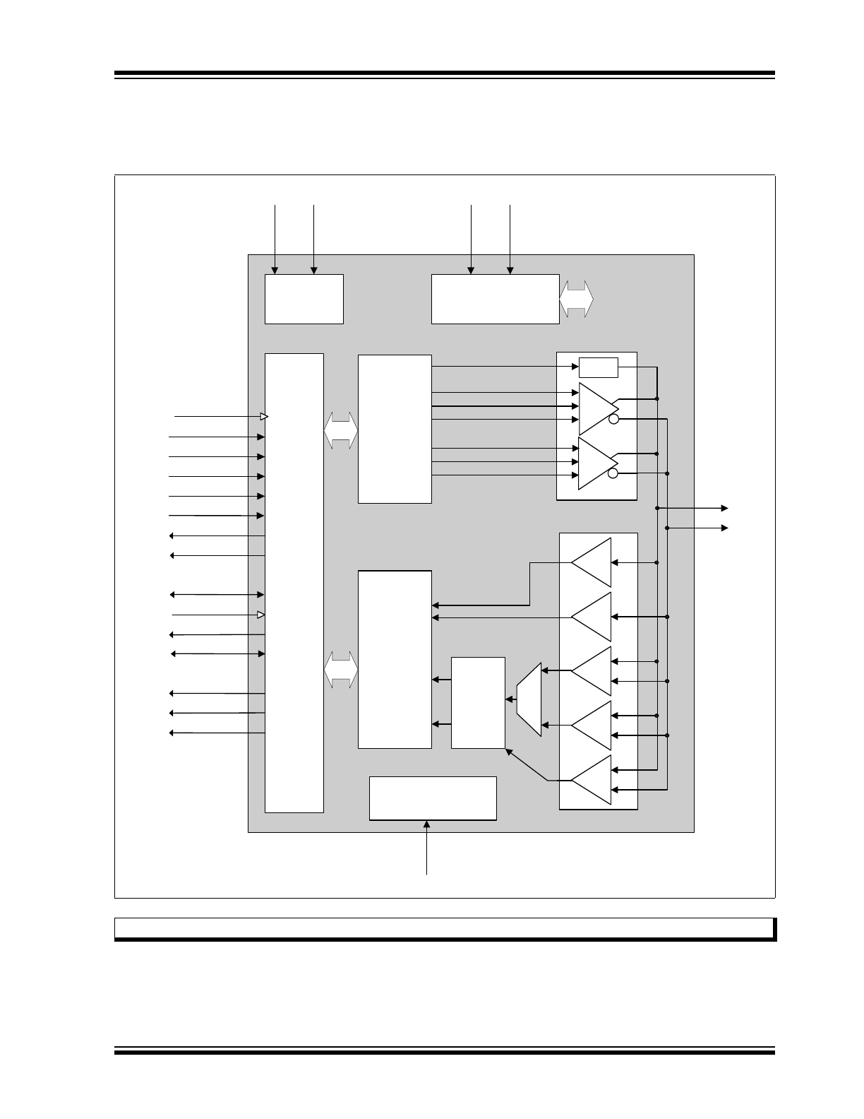
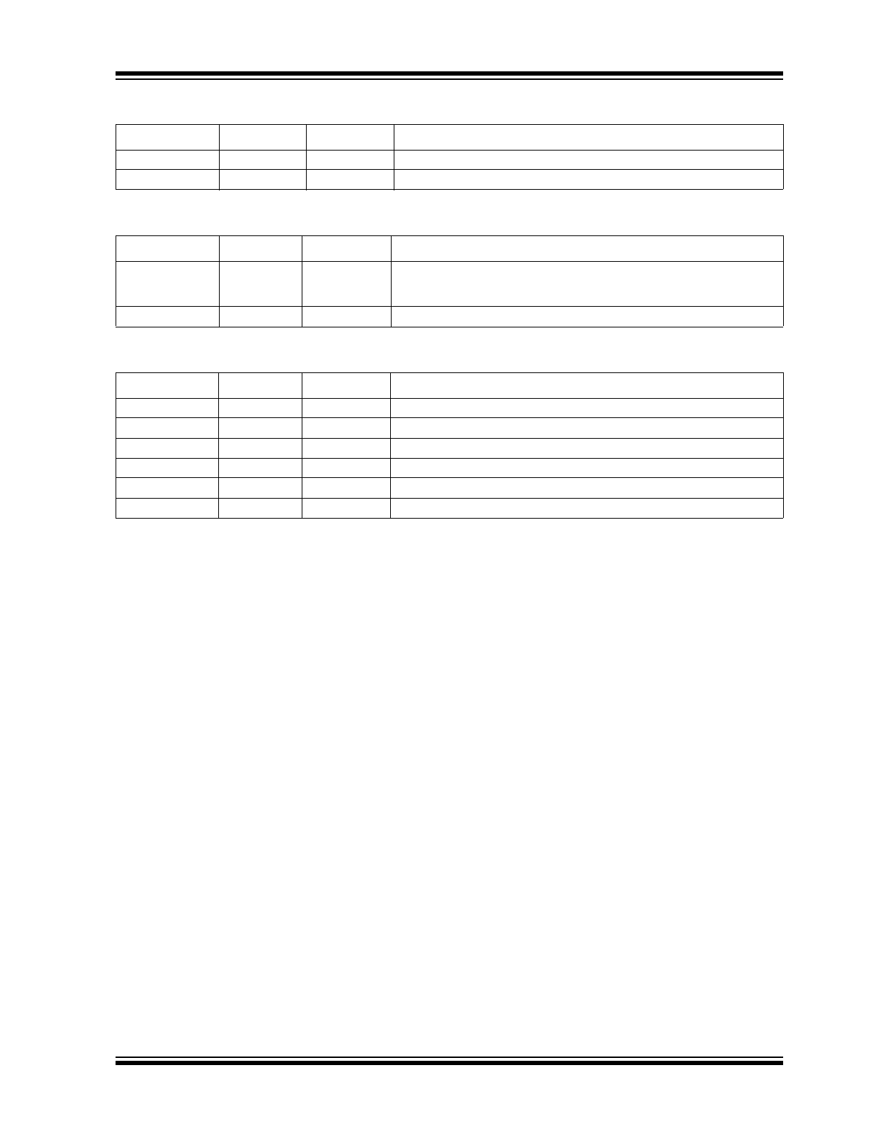
2.0
FUNCTIONAL BLOCK DIAGRAM
FIGURE 2-1:
BLOCK DIAGRAM
Note:
See
Section 7.1, "Modes of Operation," on page 19
for a description of the digital interface.
VALIDH
PWR
CONTROL
FS
SE+
RX
UT
M
I I
n
te
rf
a
ce
TX State
Machine
Parallel to
Serial
Conversion
Bit Stuff
NRZ
Encode
TX
LOGIC
Clock
Recovery Unit
Clock
and
Data
Recovery
Elasticity
Buffer
VP
VM
BIASING
Bandgap Voltage Reference
Current Reference
RB
IA
S
VD
D3
.3
VD
D1
.8
PLL and
XTAL OSC
System
Clocking
FS
RX
FS
SE-
HS
RX
HS
SQ
RX State
Machine
Serial to
Parallel
Conversion
Bit Unstuff
NRZI
Decode
RX
LOGIC
DM
TX
1.5k
FS
TX
HS
TX
HS_DATA
HS_CS_ENABLE
HS_DRIVE_ENABLE
OEB
VMO
VPO
RPU_EN
MU
X
DP
RXVALID
RXACTIVE
RXERROR
TXREADY
RESET
SUSPENDN
XCVRSELECT
TERMSELECT
OPMODE[1:0]
LINESTATE[1:0]
CLKOUT
TXVALID
DATABUS16_8
DATA[15:0] *
XI
XO
USB3250
DS00002142A-page 6
2013 - 2016 Microchip Technology Inc.
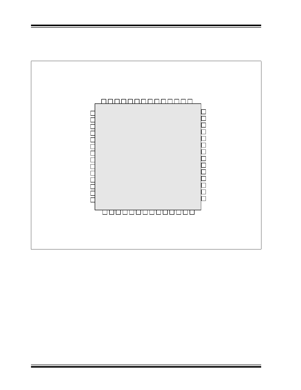
3.0
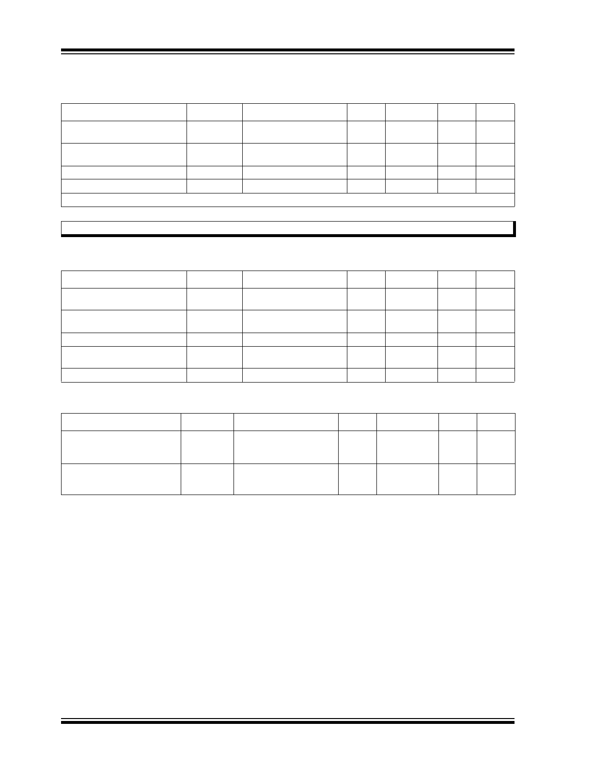
PIN CONFIGURATION
FIGURE 3-1:
56-PIN USB3250 PIN CONFIGURATION (TOP VIEW)
TE
RM
SE
L
E
C
T
L
INE
STAT
E
[1]
L
INE
STAT
E
[0]
VSS
DATA[6]
DATA[7]
DATA[8]
DATA[9]
DATA[10]
DATA[11]
DATA[12]
VSSA
DM
DP
VDDA3.3
VSSA
RBIAS
VDDA3.3
VSSA
XI
XO
VDDA1.8
SUSPENDN
VSS
VD
D3.
3
XCVRSE
LE
CT
OP
MO
DE[
1
]
OP
MO
DE[
0
]
VDD1.8
VD
D1.
8
RE
SE
T
DA
TA
[1
5
]
DA
TA
[1
4
]
DA
TA
[1
3
]
VD
D3
.3
DATA[5]
DATA[2]
DATA[3]
DATA[4]
DATA[1]
USB 2.0
USB3250
PHY IC
1
2
3
4
5
6
7
8
9
10
11
12
13
14
42
41
29
30
31
32
34
35
36
37
38
39
40
33
15
16
17
18
19
20
21
22
23
24
25
26
27
28
48
47
46
45
44
43
56
55
54
53
52
51
50
49
VD
D1
.8
VSSA
VS
S
VS
S
DA
T
A
BU
S16
_
8
VD
D1
.8
R
X
ERROR
TX
RE
AD
Y
RX
ACTI
VE
CLK
O
UT
VS
S
VA
L
IDH
RX
VA
L
ID
TX
VA
L
ID
DA
TA
[0
]
VD
D3
.3
2013 - 2016 Microchip Technology Inc.
DS00002142A-page 7
USB3250
4.0
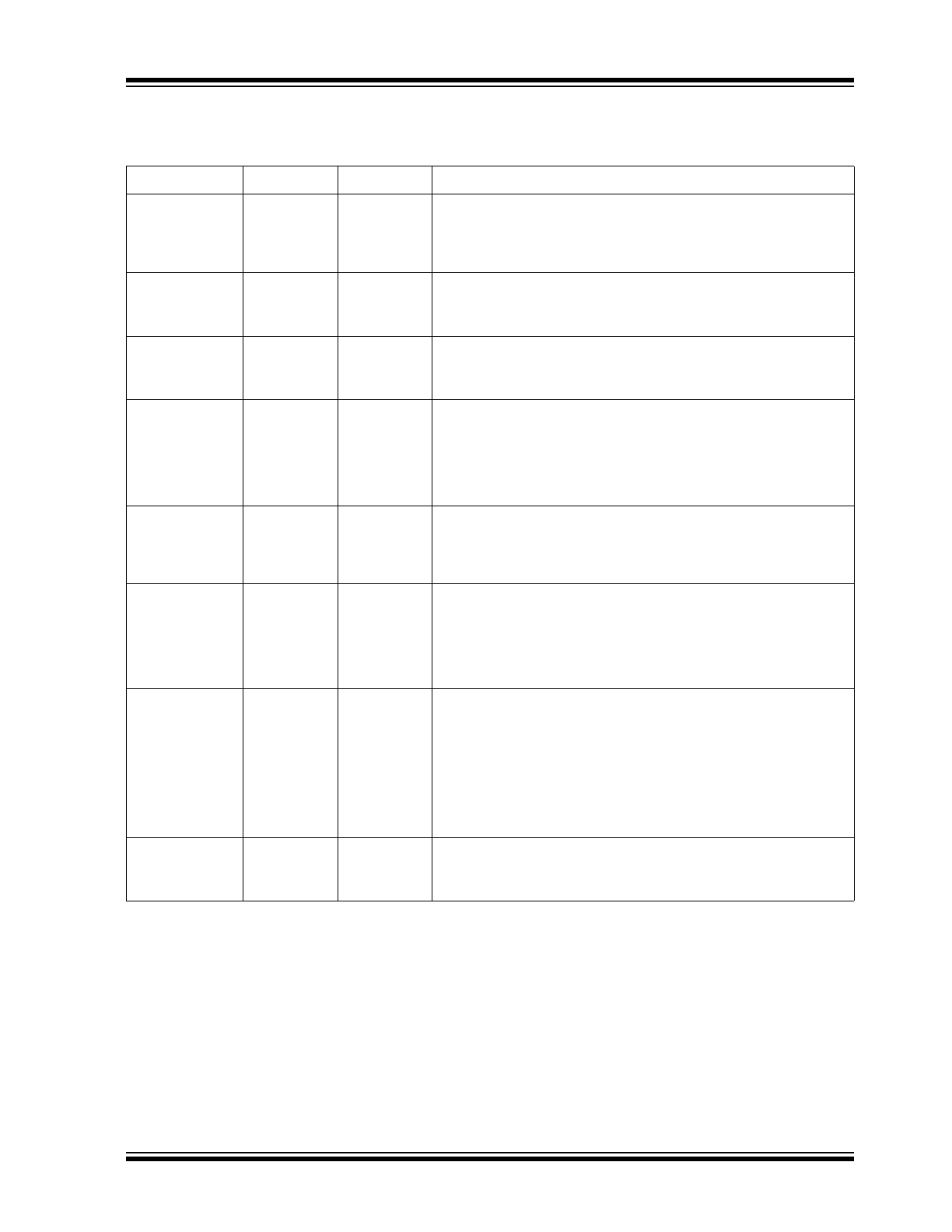
INTERFACE SIGNAL DEFINITION
TABLE 4-1:
SYSTEM INTERFACE SIGNALS
Name
Direction
Active Level
Description
RESET
Input
High
Reset. Reset all state machines. After coming out of reset, must
wait 5 rising edges of clock before asserting TXValid for transmit.
Assertion of Reset: May be asynchronous to CLKOUT.
De-assertion of Reset: Must be synchronous to CLKOUT unless
RESET is asserted longer than two periods of CLKOUT.
XCVRSELECT
Input
N/A
Transceiver Select. This signal selects between the FS and HS
transceivers:
0: HS transceiver enabled
1: FS transceiver enabled.
TERMSELECT
Input
N/A
Termination Select. This signal selects between the FS and HS
terminations:
0: HS termination enabled
1: FS termination enabled
SUSPENDN
Input
Low
Suspend. Places the transceiver in a mode that draws minimal
power from supplies. Shuts down all blocks not necessary for
Suspend/Resume operation. While suspended, TERMSELECT
must always be in FS mode to ensure that the 1.5k
pull-up on
DP remains powered.
0: Transceiver circuitry drawing suspend current
1: Transceiver circuitry drawing normal current
CLKOUT
Output
Rising Edge
System Clock. This output is used for clocking receive and
transmit parallel data at 60MHz (8-bit mode) or 30MHz (16-bit
mode). When in 8-bit mode, this specification refers to CLKOUT
as CLK60. When in 16-bit mode, CLKOUT is referred to as
CLK30.
OPMODE[1:0]
Input
N/A
Operational Mode. These signals select between the various
operational modes:
[1] [0] Description
0 0 0: Normal Operation
0 1 1: Non-driving (all terminations removed)
1 0 2: Disable bit stuffing and NRZI encoding
1 1 3: Reserved
LINESTATE[1:0]
Output
N/A
Line State. These signals reflect the current state of the USB data
bus in FS mode, with [0] reflecting the state of DP and [1]
reflecting the state of DM. When the device is suspended or
resuming from a suspended state, the signals are combinatoria.
Otherwise, the signals are synchronized to CLKOUT.
[1] [0] Description
0 0 0: SE0
0 1 1: J State
1 0 2: K State
1 1 3: SE1
DATABUS16_8
Input
N/A
Databus Select. Selects between 8-bit and 16-bit data transfers.
0 8-bit data path enabled. VALIDH is undefined. CLKOUT =
60MHz.
1: 16-bit data path enabled. CLKOUT = 30MHz.
USB3250
DS00002142A-page 8
2013 - 2016 Microchip Technology Inc.
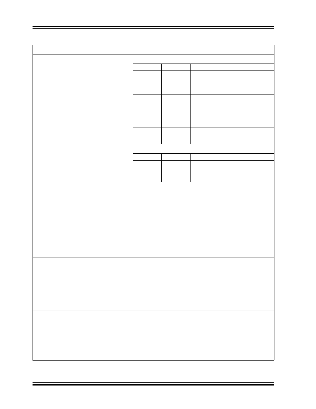
TABLE 4-2:
DATA INTERFACE SIGNALS
Name
Direction
Active Level
Description
DATA[15:0]
Bidir
N/A
DATA BUS. 16-BIT BIDIRECTIONAL MODE.
TXVALID
RXVALID
VALIDH
DATA[15:0]
0
0
X
Not used
0
1
0
DATA[7:0] output is valid
for receive
VALIDH is an output
0
1
1
DATA[15:0] output is
valid for receive
VALIDH is an output
1
X
0
DATA[7:0] input is valid
for transmit
VALIDH is an input
1
X
1
DATA[15:0] input is valid
for transmit
VALIDH is an input
DATA BUS. 8-BIT UNIDIRECTIONAL MODE.
TXVALID
RXVALID
DATA[15:0]
0
0
Not used
0
1
DATA[15:8] output is valid for receive
1
X
DATA[7:0] input is valid for transmit
TXVALID
Input
High
Transmit Valid. Indicates that the TXDATA bus is valid for
transmit. The assertion of TXVALID initiates the transmission of
SYNC on the USB bus. The negation of TXVALID initiates EOP on
the USB.
Control inputs (OPMODE[1:0], TERMSELECT,XCVRSELECT)
must not be changed on the de-assertion or assertion of TXVALID.
The PHY must be in a quiescent state when these inputs are
changed.
TXREADY
Output
High
Transmit Data Ready. If TXVALID is asserted, the SIE must
always have data available for clocking into the TX Holding
Register on the rising edge of CLKOUT. TXREADY is an
acknowledgment to the SIE that the transceiver has clocked the
data from the bus and is ready for the next transfer on the bus. If
TXVALID is negated, TXREADY can be ignored by the SIE.
VALIDH
Bidir
N/A
Transmit/Receive High Data Bit Valid (used in 16-bit mode
only). When TXVALID = 1, the 16-bit data bus direction is changed
to inputs, and VALIDH is an input. If VALIDH is asserted,
DATA[15:0] is valid for transmission. If deasserted, only DATA[7:0]
is valid for transmission. The DATA bus is driven by the SIE.
When TXVALID = 0 and RXVALID = 1, the 16-bit data bus direction
is changed to outputs, and VALIDH is an output. If VALIDH is
asserted, the DATA[15:0] outputs are valid for receive. If
deasserted, only DATA[7:0] is valid for receive. The DATA bus is
read by the SIE.
RXVALID
Output
High
Receive Data Valid. Indicates that the RXDATA bus has received
valid data. The Receive Data Holding Register is full and ready to
be unloaded. The SIE is expected to latch the RXDATA bus on the
rising edge of CLKOUT.
RXACTIVE
Output
High
Receive Active. Indicates that the receive state machine has
detected Start of Packet and is active.
RXERROR
Output
High
Receive Error. 0: Indicates no error. 1: Indicates a receive error
has been detected. This output is clocked with the same timing as
the RXDATA lines and can occur at anytime during a transfer.
2013 - 2016 Microchip Technology Inc.
DS00002142A-page 9
USB3250
Note 4-1
A Ferrite Bead (with DC resistance <.5 Ohms) is recommended for filtering between both the VDD3.3
and VDDA3.3 supplies and the VDD1.8 and VDDA1.8 Supplies. See
FIGURE 8-9: Application
Diagram for 56-pin VQFN Package on page 39
.
Note 4-2
All VSS and VSSA are bonded to the exposed pad under the IC in the package. The exposed pad
must be connected to solid GND plane on printed circuit board.
TABLE 4-3:
USB I/O SIGNALS
Name
Direction
Active Level
Description
DP
I/O
N/A
USB Positive Data Pin.
DM
I/O
N/A
USB Negative Data Pin.
TABLE 4-4:
BIASING AND CLOCK OSCILLATOR SIGNALS
Name
Direction
Active Level
Description
RBIAS
Input
N/A
External 1% bias resistor. Requires a 12K
resistor to ground.
Used for setting HS transmit current level and on-chip termination
impedance.
XI/XO
Input
N/A
External crystal. 12MHz crystal connected from XI to XO.
TABLE 4-5:
POWER AND GROUND SIGNALS
Name
Direction
Active Level
Description
VDD3.3
N/A
N/A
3.3V Digital Supply. Powers digital pads. See
Note 4-1
VDD1.8
N/A
N/A
1.8V Digital Supply. Powers digital core.
VSS
N/A
N/A
Digital Ground. See
Note 4-2
VDDA3.3
N/A
N/A
3.3V Analog Supply. Powers analog I/O and 3.3V analog circuitry.
VDDA1.8
N/A
N/A
1.8V Analog Supply. Powers 1.8V analog circuitry. See
Note 4-1
VSSA
N/A
N/A
Analog Ground. See
Note 4-2
USB3250
DS00002142A-page 10
2013 - 2016 Microchip Technology Inc.
5.0
LIMITING VALUES
Note 5-1
The USB 2.0 Specification requires a frequency accuracy of +/-500ppm. For applications using a
quartz crystal, Microchip recommends that it be specified with an accuracy of +/-100ppm. Resonators
that are specified to meet the +/-500ppm accuracy have also been used successfully with the
USB3250.
FIGURE 5-1:
ABSOLUTE MAXIMUM RATINGS
Parameter
Symbol
Conditions
MIN
TYP
MAX
Units
1.8V Supply Voltage
(VDD1.8 and VDDA1.8)
V
DD1.8
-0.5
TBD
V
3.3V Supply Voltage
(VDD3.3 and VDDA3.3)
V
DD3.3
-0.5
4.6
V
Input Voltage
V
I
-0.5
4.6
V
Storage Temperature
T
STG
-40
+125
o
C
[1] Equivalent to discharging a 100pF capacitor via a 1.5k
resistor (HBM).
Note:
In accordance with the Absolute Maximum Rating System (IEC 60134).
FIGURE 5-2:
RECOMMENDED OPERATING CONDITIONS
Parameter
Symbol
Conditions
MIN
TYP
MAX
Units
1.8V Supply Voltage
(VDD1.8 and VDDA1.8)
V
DD1.8
1.6
1.8
2.0
V
3.3V Supply Voltage
(VDD3.3 and VDDA3.3)
V
DD3.3
3.0
3.3
3.6
V
Input Voltage on Digital Pins
V
I
0.0
V
DD3.3
V
Input Voltage on Analog I/O
Pins (DP, DM)
V
I(I/O)
0.0
V
DD3.3
V
Ambient Temperature
T
A
-40
+85
o
C
FIGURE 5-3:
RECOMMENDED EXTERNAL CLOCK CONDITIONS
Parameter
Symbol
Conditions
MIN
TYP
MAX
Units
System Clock Frequency
XO driven by the external
clock; and no connection
at XI
12
(+/- 100ppm)
Note 5-1
MHz
System Clock Duty Cycle
XO driven by the external
clock; and no connection
at XI
45
50
55
%