

2014-2018 Microchip Technology Inc.
DS00001578D-page 1
General Description
The USB2642 is a USB 2.0 compliant, hi-speed hub
and card reader combo solution. This fully-integrated,
single chip solution provides USB expansion and flash
media reader/writer integration. The Microchip
USB2642 provides an ultra fast interface between a
USB host and today’s popular flash media formats. The
controller allows read/write capability to flash media
including the following:
• Secure Digital
TM
(SD)
• SD High Capacity
TM
(SDHC)
• SD Extended Capacity
TM
(SDXC)
• MultiMediaCard
TM
(MMC)
• Embedded MultiMediaCard
TM
(eMMC)
The USB2642 offers a versatile, cost-effective and
energy-efficient hub controller with 2 downstream USB
2.0 ports and a flash media interface. The flash media
interface can support sustained transfer rates exceed-
ing 35 MB/s.
Additionally, the USB2642 provides an I
2
C
TM
over USB
bridge and an SD over USB bridge. The I
2
C bridge
allows for control of any I
2
C slave device operating at
50KHz serial clock.
Highlights
• PortMap
- Flexible port mapping and port disable
sequencing supports multiple platform
designs
• PortSwap
- Programmable USB differential-pair pin loca-
tions eases PCB design by aligning USB sig-
nal traces directly to connectors
• PHYBoost
- Programmable USB transceiver drive
strength recovers signal integrity
Features
• Single-chip USB 2.0 hub controller with 2
exposed hi-speed downstream ports
• The dedicated flash media reader is internally
attached to a 3rd downstream port of the hub as a
USB compound device
• Hub and flash media reader/writer configuration
from a single source:
- Configures internal code using an external
SPI ROM
- Supports execution of external code from SPI
Flash EEPROM
- Supports custom vendor, product, and lan-
guage ID when using an external EEPROM
• Supports full power management with individual
or ganged power control of each downstream port
• Transaction Translator (TT) in the hub supports
operation of FS and LS peripherals
• Single 24 MHz crystal support
• Control of peripheral I
2
C devices by USB host.
• Supports internally or externally regulated 1.8 V
core voltage operation
• Supports storage addressability of up to 2TB
• RoHS compliant package
- USB2642: 48-pin (7x7 mm²) QFN
• Temperature ranges:
- Commercial Range (0 ºC to +70 ºC)
- Industrial Range (-40 ºC to +85 ºC)
Target Applications
• Desktop and mobile PCs
• Monitors and televisions
• Mobile PC docking
• Consumer A/V
• Media players/viewers
• Printers
• Flash media card readers/writers
USB2642
USB 2.0 Hub and Flash Media Card Controller Combo

USB2642
DS00001578D-page 2
2014-2018 Microchip Technology Inc.
TO OUR VALUED CUSTOMERS
It is our intention to provide our valued customers with the best documentation possible to ensure successful use of your Microchip
products. To this end, we will continue to improve our publications to better suit your needs. Our publications will be refined and
enhanced as new volumes and updates are introduced.
If you have any questions or comments regarding this publication, please contact the Marketing Communications Department via
E-mail at
docerrors@microchip.com
. We welcome your feedback.
Most Current Data Sheet
To obtain the most up-to-date version of this data sheet, please register at our Worldwide Web site at:
http://www.microchip.com
You can determine the version of a data sheet by examining its literature number found on the bottom outside corner of any page.
The last character of the literature number is the version number, (e.g., DS30000000A is version A of document DS30000000).
Errata
An errata sheet, describing minor operational differences from the data sheet and recommended workarounds, may exist for cur-
rent devices. As device/documentation issues become known to us, we will publish an errata sheet. The errata will specify the
revision of silicon and revision of document to which it applies.
To determine if an errata sheet exists for a particular device, please check with one of the following:
• Microchip’s Worldwide Web site;
http://www.microchip.com
• Your local Microchip sales office (see last page)
When contacting a sales office, please specify which device, revision of silicon and data sheet (include -literature number) you are
using.
Customer Notification System
Register on our web site at
www.microchip.com
to receive the most current information on all of our products.

2014-2018 Microchip Technology Inc.
DS00001578D-page 3
USB2642
Table of Contents
1.0 Overview ......................................................................................................................................................................................... 4
2.0 Block Diagram ................................................................................................................................................................................. 6
3.0 USB2642 Pin Configuration ............................................................................................................................................................ 7
4.0 Pin Table ......................................................................................................................................................................................... 8
5.0 Pin Descriptions .............................................................................................................................................................................. 9
6.0 Pin Reset States ........................................................................................................................................................................... 17
7.0 Configuration Options ................................................................................................................................................................... 19
8.0 DC Parameters ............................................................................................................................................................................. 42
9.0 AC Specifications .......................................................................................................................................................................... 46
10.0 Package Outlines ........................................................................................................................................................................ 48
11.0 Revision History .......................................................................................................................................................................... 50
Appendix A: Acronyms ........................................................................................................................................................................ 51
Appendix B: References ..................................................................................................................................................................... 52
The Microchip Web Site ...................................................................................................................................................................... 53
Customer Change Notification Service ............................................................................................................................................... 53
Customer Support ............................................................................................................................................................................... 53
Product Identification System ............................................................................................................................................................. 54
USB2642
DS00001578D-page 4
2014-2018 Microchip Technology Inc.
1.0
OVERVIEW
1.1
Introduction
The USB2642 offers a USB 2.0 compliant, versatile, cost-effective and energy-efficient hi-speed hub controller with 2
downstream USB ports and an SD/MMC flash media card interface. The dedicated flash media reader is internally
attached to a 3rd downstream port of the hub as a USB compound device. This combo solution supports today’s popular
multi-format flash media card formats. The flash media interface can support sustained transfer rates exceeding 35 MB/
s if the media and host support those rates.
The USB2642 also provides I
2
C over USB. The I
2
C bridge allows for control of any I
2
C device operating at 50kHz clock.
The USB2642 will attach to an upstream port as either a full-speed or full-/hi-speed hub. The hub supports low-speed,
full-speed, and hi-speed (if operating as a full-/hi-speed hub) downstream devices on all of the enabled downstream
ports.
All required resistors on the USB ports are integrated into the hub. This includes all series termination resistors on D+
and D- pins and all required pull-down and pull-up resistors. The over-current sense inputs for the downstream facing
ports have internal pull-up resistors.
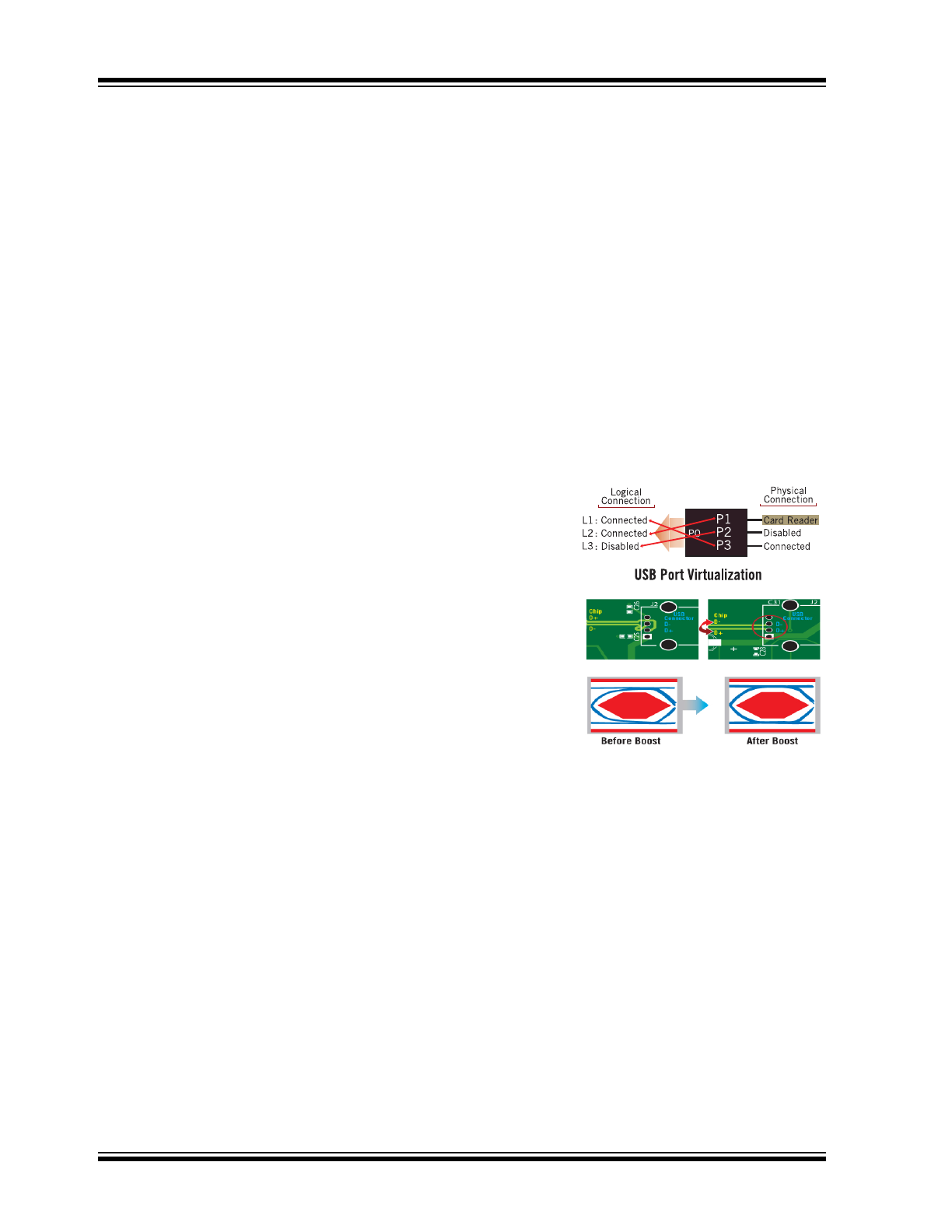
The USB2642 includes programmable features such as:
PortMap
which provides flexible port mapping and disable sequences. The downstream ports of a USB2642 hub can
be reordered or disabled in any sequence to support multiple platform designs with minimum effort. For any port that is
disabled, the USB2642 automatically reorders the remaining ports to match
the USB host controller’s port numbering scheme.
PortSwap
which adds per-port programmability to USB differential-pair pin
locations. PortSwap allows direct alignment of USB signals (D+/D-) to con-
nectors avoiding uneven trace length or crossing of the USB differential sig-
nals on the PCB.
PHYBoost
which enables four programmable levels of USB signal drive
strength in downstream port transceivers. PHYBoost attempts to restore USB
signal integrity. The diagram on the right shows an example of Hi-Speed USB
eye diagrams before (PHYBoost at 0%) and after (PHYBoost at 12%) signal
integrity restoration in a compromised system environment.

2014-2018 Microchip Technology Inc.
DS00001578D-page 5
USB2642
1.2
Device Features
1.2.1
HARDWARE FEATURES
• Single-chip hub, flash media controller, and I
2
C device control over USB
• Supports commercial (0 °C to +70 °C) and industrial (-40 °C to +85 °C) temperature ranges
• Transaction Translator (TT) in the hub supports operation of FS and LS peripherals
• Full power management with individual or ganged power control of each downstream port
• Optional support for external firmware access via SPI
• Code execution via SPI ROM which must meet the following qualifications:
- 60 MHz operation support
- Single bit or dual bit mode support
- Mode 0 or mode 3 SPI support
Compliant with the following flash media card specifications:
• Secure Digital 2.0
- SDSC, SDHC, and SDXC
- microSD and reduced form factor media
- Supports storage addressability of up to 2TB
• MultiMediaCard 4.2
- 1/4/8 bit
- Includes support for eMMC devices
• Control of I
2
C device using the I
2
C over USB bridge
• Supports internal regulator for 1.8 V core operation
• Supports external regulator for 1.8 V core operation
1.2.2
CONFIGURABLE FEATURES
Default configuration is loaded by USB2642 following a reset. The USB2642 may also be configured by an external I
2
C
EEPROM or external SPI ROM flash, where the following features are supported:
• Customizable vendor ID, product ID, and device ID
• 12-hex digits maximum for the serial number string
• 29-character manufacturer ID and product strings for flash media reader/writer
• Compound device support on a port-by-port basis a port is permanently hardwired to a downstream USB periph-
eral device
• Select over-current sensing and port power control on an individual or ganged (all ports together) basis to match
the circuit board component selection
• Port power control and over-current detection/delay features
• Configure the delay time for filtering the over-current sense inputs
• Configure the delay time for turning on downstream port power
• Bus- or self-powered selection
• Hub port disable of non-removable configurations
• Flexible port mapping and disable sequencing supports multiple platform designs
• Programmable USB differential-pair pin location selection eases PCB layout by aligning USB signal lines directly
to connectors
• Programmable USB signal drive strength improves USB signal integrity using 4 levels of signal drive strength
• Indicate the maximum current that the 2-port hub consumes from the USB upstream port
• Manage the maximum current required for the hub controller
USB2642
DS00001578D-page 6
2014-2018 Microchip Technology Inc.
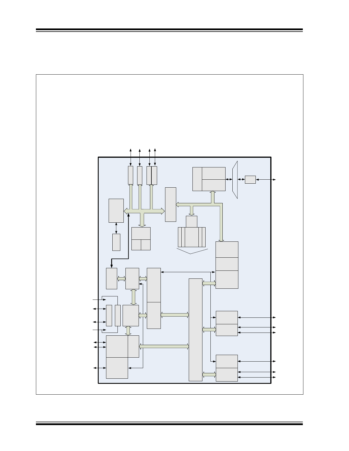
2.0
BLOCK DIAGRAM
FIGURE 2-1:
USB2642 BLOCK DIAGRAM
T
o
U
p
st
re
am
V
BUS
3.
3 V
U
p
s
tream
PH
Y
U
p
st
ream
U
S
B
Da
ta
R
e
p
eat
er
Contr
o
ll
e
r
Se
ri
a
l
Int
e
rf
ace
Engi
ne
Se
ri
a
l
Int
e
rf
ace
PL
L
24 M
H
z
C
ryst
al
Routi
n
g
&
P
o
rt Re
-Orde
ri
ng Lo
gi
c
Port
C
o
ntro
ll
e
r
PHY
Po
rt
#3
OC
Se
nse
Swi
tc
h
Dr
iv
e
r
B
u
s-
Power
De
te
c
t/
V
BU
S
Pu
lse
1.
8
V
T
ra
n
sact
io
n
Tran
slat
o
r
1.
8
V
R
e
g
PHY
Po
rt
#2
OC
Se
nse
Swi
tc
h
Dr
iv
e
r
USB Da
ta
D
o
w
n
s
tream
O
C
S
e
n
se/
Pwr
S
w
it
ch
8051
P
R
O
C
ES
SO
R
SFR
RA
M
XDA
T
A BR
ID
GE
+ B
U
S ARB
IT
E
R
RO
M
64K
RA
M
6K
ADD
R
MAP
P
W
R_FET0
Pro
g
ra
m
Me
mor
y
I/O
B
u
s
GPO
1
(CR
D
_
P
WR
)
GP
IO
s
3 K
to
ta
l
RA
M
EP
2 T
X
EP
2 R
X
BUS
IN
TFC
EP
0 R
X
EP
0 T
X
EP
2 R
X
SI
E
CTL
BR
ID
GE
BU
S
IN
TF
C
FMD
U
CT
L
AU
T
O
_
C
BW
PR
O
C
FMI
BUS
IN
TFC
USB Da
ta
D
o
w
n
st
ream
SD
/
MMC
O
C
S
e
nse/
Pw
r S
w
it
ch
SP
I
SP
I (4
pin
s
)
S
D
/MMC
S
o
c
k
e
t
e
MMM I
C
I2
C
I2
C (2
pi
ns)
2014-2018 Microchip Technology Inc.
DS00001578D-page 7
USB2642
3.0
USB2642 PIN CONFIGURATION
FIGURE 3-1:
USB2642 48-PIN QFN - TOP VIEW
USB2642
RESET_N
38
VBUS_DET
39
GPO1
37
TEST0
40
VDDA33
41
USBUP_DM
43
XTAL2
44
XTAL1 (CLKIN)
45
RBIAS
48
VDDA33
47
VDD18PLL
46
USBUP_DP
42
VD
DA33
1
US
BD
N_D
M
2
2
US
BDN_
D
P
2
3
US
BD
N_D
M
3
4
US
BDN_
D
P
3
5
PR
TC
T
L
2
6
PR
TC
T
L
3
7
SP
I_C
E
_N
8
SP
I_
C
L
K/
SC
L
_
E
P
9
V
DD33
10
SP
I_D
I
11
S
P
I_DO/
S
DA_EP/
S
P
I_S
PD_S
EL
12
21
SD_CLK
20
SD_D6
19
SD_D7
18
SD_D0
17
VDD18
16
SD_D1
15
VDD33
14
SD_nCD
13
SD_WP
23
SD_D5
22
REG_EN
24
SD_CMD
35
SC
L
34
CRD
_
P
WR
33
VDD
3
3
32
SD
_D3
31
NC
30
SD
_D4
29
SD
A
28
TES
T2
36
SD
_D2
27
TES
T1
26
VDD
3
3
(
O
TP)
25
VDD
3
3
Indicates pins on the bottom of the device.
3
e
Ground Pad
(must be connected
to VSS)
USB2642
DS00001578D-page 8
2014-2018 Microchip Technology Inc.
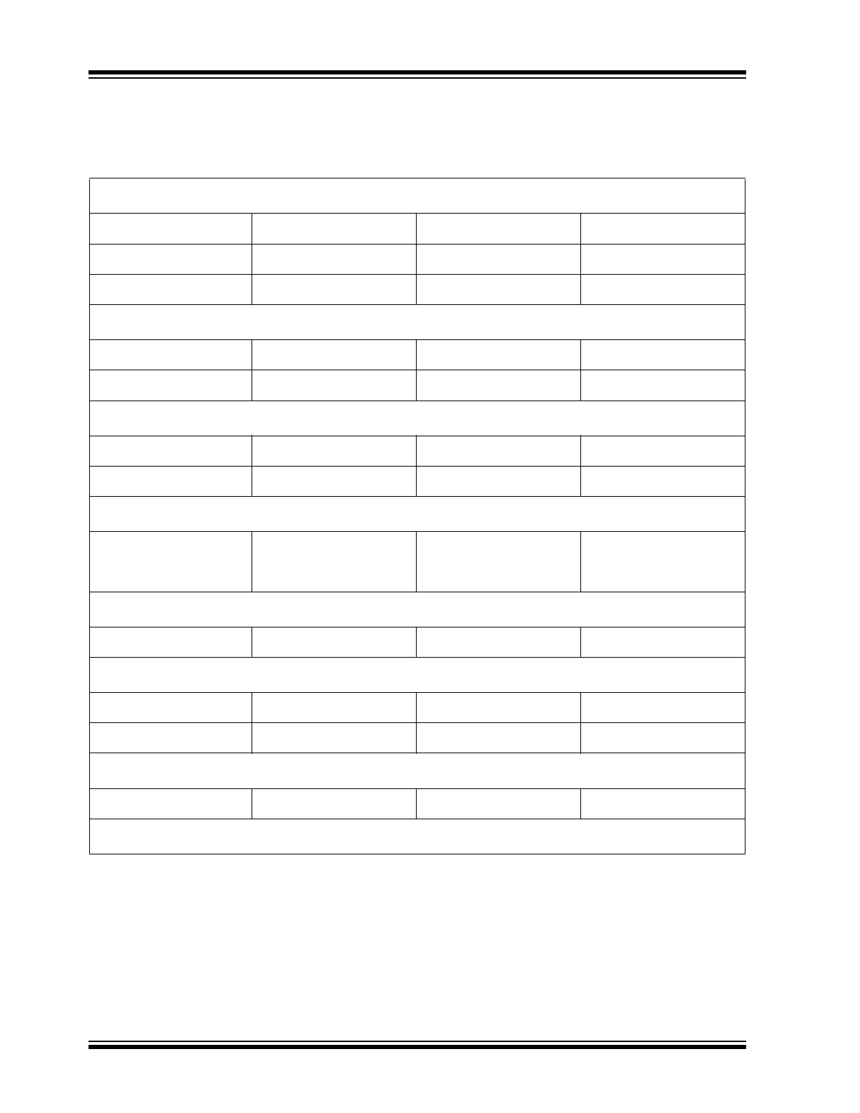
4.0
PIN TABLE
TABLE 4-1:
USB2642 48-PIN TABLE (GROUPED BY FUNCTION)
Secure Digital (12 pins)
SD_D7
SD_D6
SD_D5
SD_D4
SD_D3
SD_D2
SD_D1
SD_D0
SD_CLK
SD_CMD
SD_nCD
SD_WP
USB 2.0 Interface (10 pins)
USBUP_DP
USBUP_DM
XTAL1 (CLKIN)
XTAL2
RBIAS
(3) VDDA33
VDD18PLL
REG_EN
2-PORT USB Interface (7 pins)
USBDN_DP2
USBDN_DM2
PRTCTL2
PRTCTL3
USBDN_DP3
USBDN_DM3
VBUS_DET
-
SPI Interface (4 pins)
SPI_CE_N
SPI_CLK/
SCL_EP
SPI_DO/
SDA_EP/
SPI_SPD_SEL
SPI_DI
I
2
C Interface (2 pins)
SCL
SDA
MISC (7 pins)
RESET_N
TEST0
TEST1
TEST2
GPO1
CRD_PWR
(1) NC
POWER (6 pins)
(4) VDD33
VDD33
VDD18
Total 48
2014-2018 Microchip Technology Inc.
DS00001578D-page 9
USB2642
5.0
PIN DESCRIPTIONS
This section provides a detailed description of each signal. The signals are arranged in functional groups according to
their associated interface. The pin descriptions below are applied when using the internal default firmware and can be
referenced in
Section 7.0, Configuration Options
. The acronyms used in this chapter can be referenced in
Appendix A:
"Acronyms"
.
An N at the end of a signal name indicates that the active (asserted) state occurs when the signal is at a low voltage
level. When the N is not present, the signal is asserted when it is at a high voltage level. The terms assertion and nega-
tion are used exclusively in order to avoid confusion when working with a mixture of active low and active high signals.
The term assert, or assertion, indicates that a signal is active, independent of whether that level is represented by a high
or low voltage. The term negate, or negation, indicates that a signal is inactive.
5.1
USB2642 Pin Description
TABLE 5-1:
USB2642 PIN DESCRIPTIONS
Symbol
48-Pin
QFN
Buffer
Type
Description
Secure Digital Interface
SD_D[7:0]
19
20
23
30
32
33
17
18
I/O12PU
Secure Digital Data 7-0
These are the bi-directional data signals SD_D0 - SD_D7
Note:
The pull up resistance is a current source that is limited to VDD.
SD_CLK
21
O12
Secure Digital Clock
This is an output clock signal to SD/MMC device.
SD_CMD
24
I/O12PU
Secure Digital Command
This is a bi-directional signal that connects to the CMD signal of the SD/
MMC device.
SD_nCD
14
I/O12PU
Secure Digital Card Detect
SD_WP
13
I/O12
Secure Digital Write Protect
I
2
C Interface
SDA
29
I/O12
Serial Data Signal
SCL
36
I/O12
Serial Clock
USB Interface
USBUP_DM
USBUP_DP
43
42
I/O-U
USB Bus Data
These pins connect to the upstream USB bus data signals (host port or
upstream hub). USBUP_DM and USBUP_DP can be swapped using the
PortSwap feature.
USBDN_DM
[3:2]
USBDN_DP
[3:2]
3
1
4
2
I/O-U
USB Bus Data
These pins connect to the downstream USB bus data signals and can be
swapped using the PortSwap feature.
USB2642
DS00001578D-page 10
2014-2018 Microchip Technology Inc.
PRTCTL[3:2]
7
6
I/OD12PU USB Power Enable
As an output, these pins enables power downstream USB peripheral
devices. See
Section 5.3, "Port Power Control"
for diagram and usage
instructions.
As an input, when the power is enabled, these pins monitor the over-
current condition. When an over-current condition is detected, these pins
turn the power off.
VBUS_DET
39
I
Detect Upstream VBUS Power
The Microchip hub monitors VBUS_DET to determine when to assert the
internal D+ pull-up resistor (signaling a connect event).
When designing a detachable hub, connect this pin to the VBUS power
pin of the USB port that is upstream of the hub.
For self-powered applications with a permanently attached host, this pin
should be pulled up, typically to VDD33.
VBUS is a 3.3 volt input. A resistor divider must be used when connecting
to 5 volts of USB power.
RBIAS
47
I-R
USB Transceiver Bias
A 12.0 kΩ,
±
1.0% resistor is attached from VSS to this pin in order to set
the transceiver's internal bias currents.
XTAL1 (CLKIN)
45
ICLKx
24 MHz Crystal Input/External Clock Input
This pin can be connected to one terminal of the crystal or it can be
connected to an external 24 MHz clock when a crystal is not used.
XTAL2
44
OCLKx
24 MHz Crystal Output
This is the other terminal of the crystal, or a no connect pin, when an
external clock source is used to drive XTAL1 (CLKIN).
VDD18PLL
46
-
1.8 V PLL Power Bypass
This pin is the 1.8 V power bypass for the PLL. This pin requires an
external bypass capacitor of 1.0 µF.
If REG_EN is low, this pin serves as a power supply (1.8 V) for the device.
VDDA33
5
41
48
-
3.3 V Analog Power
• 48QFN - Pin 48 requires an external bypass capacitor of 4.7 µF.
SPI Interface
SPI_CE_N
8
O12
SPI Chip Enable
This is the active low chip enable output. If the SPI interface is enabled,
drive this pin high in power down states.
SPI_CLK/
9
I/O12
SPI Clock
This is the SPI clock out to the serial ROM. See
Section 5.4, "ROM Boot
Sequence"
for diagram and usage instructions.
During reset, this pin is driven low.
SCL_EP
When configured, this is the I²C EEPROM clock pin.
TABLE 5-1:
USB2642 PIN DESCRIPTIONS
Symbol
48-Pin
QFN
Buffer
Type
Description