

2013 - 2015 Microchip Technology Inc.
DS00001726B-page 1
General Description
The Microchip USB2422 hub is a low-power, single
transaction translator, hub controller IC with two down-
stream ports for embedded USB solutions. The hub
controller can attach to an upstream port as a Hi-Speed
and Full-Speed hub or as a Full-Speed only hub. The
hub supports Low-Speed, Full-Speed, and Hi-Speed
(when configured as a Hi-Speed hub) downstream
devices on the enabled downstream ports.
All required resistors on the USB ports are integrated
into the hub. This includes all series termination resis-
tors on D+ and D- pins and all required pull-down and
pull-up resistors on D+ and D- pins. The over-current
sense inputs for the downstream facing ports have
internal pull-up resistors.
Features
• Supports the USB Battery Charging Specification,
Revision 1.1
• Fully integrated USB termination and pull-up/pull-
down resistors
• Supports a single external 3.3 V supply source;
internal regulators provide 1.2 V internal core volt-
age
• On-chip driver for 24 MHz crystal resonator or
external 24 MHz clock input
• ESD protection up to 6 kV on all USB pins
• Supports self-powered operation
• The hub contains a built-in default configuration;
no external configuration options or components
are required
• Downstream ports as non-removable ports
• Downstream port power control and over-current
detection on an individual or ganged basis
• Supports compound devices on a port-by-port
basis
• 24-pin SQFN (4x4 mm), RoHS-compliant pack-
age
• Commercial temperature range support:
0ºC to +70ºC
• Industrial temperature range support:
-40ºC to +85ºC
Highlights
• High performance, low-power, small footprint hub
controller IC with two downstream ports
• Fully compliant with the USB 2.0 Specification
• Optimized for minimal bill-of-materials and low-
cost designs
Applications
• LCD monitors and TVs
• Multi-function USB peripherals
• PC motherboards
• Set-top boxes, DVD players, DVR/PVR
• Printers and scanners
• PC media drive bay
• Portable hub boxes
• Mobile PC docking
• Embedded systems
• Gaming consoles
• Cable/DSL modems
• HDD enclosures
• KVM switches
• Server front panels
• Point-of-Sale (POS) systems
• IP telephony
• Automobile/home audio systems
• Thin client terminals
USB2422
2-Port USB 2.0 Hi-Speed Hub Controller

USB2422
DS00001726B-page 2
2013 - 2015 Microchip Technology Inc.
TO OUR VALUED CUSTOMERS
It is our intention to provide our valued customers with the best documentation possible to ensure successful use of your Microchip
products. To this end, we will continue to improve our publications to better suit your needs. Our publications will be refined and
enhanced as new volumes and updates are introduced.
If you have any questions or comments regarding this publication, please contact the Marketing Communications Department via
E-mail at
docerrors@microchip.com
. We welcome your feedback.
Most Current Data Sheet
To obtain the most up-to-date version of this data sheet, please register at our Worldwide Web site at:
http://www.microchip.com
You can determine the version of a data sheet by examining its literature number found on the bottom outside corner of any page.
The last character of the literature number is the version number, (e.g., DS30000000A is version A of document DS30000000).
Errata
An errata sheet, describing minor operational differences from the data sheet and recommended workarounds, may exist for cur-
rent devices. As device/documentation issues become known to us, we will publish an errata sheet. The errata will specify the
revision of silicon and revision of document to which it applies.
To determine if an errata sheet exists for a particular device, please check with one of the following:
• Microchip’s Worldwide Web site;
http://www.microchip.com
• Your local Microchip sales office (see last page)
When contacting a sales office, please specify which device, revision of silicon and data sheet (include -literature number) you are
using.
Customer Notification System
Register on our web site at
www.microchip.com
to receive the most current information on all of our products.

2013 - 2015 Microchip Technology Inc.
DS00001726B-page 3
USB2422
Table of Contents
1.0 Block Diagram ................................................................................................................................................................................. 4
2.0 Pin Descriptions .............................................................................................................................................................................. 6
3.0 Battery Charging Support ............................................................................................................................................................. 14
4.0 Configuration Options ................................................................................................................................................................... 16
5.0 DC Parameters ............................................................................................................................................................................. 35
6.0 AC Specifications .......................................................................................................................................................................... 38
7.0 Package Outline ............................................................................................................................................................................ 40
Appendix A: Acronyms ........................................................................................................................................................................ 41
Appendix B: References ..................................................................................................................................................................... 42
Appendix C: Data Sheet Revision History .......................................................................................................................................... 43
The Microchip Web Site ...................................................................................................................................................................... 44
Customer Change Notification Service ............................................................................................................................................... 44
Customer Support ............................................................................................................................................................................... 44
Product Identification System ............................................................................................................................................................. 45
USB2422
DS00001726B-page 4
2013 - 2015 Microchip Technology Inc.
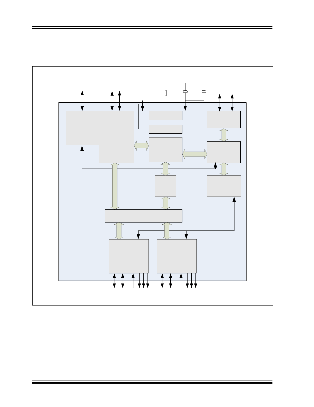
1.0
BLOCK DIAGRAM
FIGURE 1-1:
USB2422 BLOCK DIAGRAM
To Upstream
V
BUS
3.3V
Upstream
PHY
Upstream USB
Data
Repeater
Controller
SIE
Serial
Interface
PLL
24 MHz Crystal
To
SMBus Master
Routing & Port Re-Ordering
Logic
SMBCLK
SMBDATA
Port
Controller
Bus-Power
Detect/V
BUS
Pulse
TT
PHY#1
Port #1
OC
Sense
Switch
Driver
PHY#2
Port #2
OC
Sense
Switch
Driver
USB Data
Downstream
OC Sense
Switch
USB Data
Downstream
OC Sense
Switch
CRFILT PLLFILT
1.2V Reg

2013 - 2015 Microchip Technology Inc.
DS00001726B-page 5
USB2422
Within this manual, the following abbreviations and symbols are used to improve readability.
Example
Description
BIT
Name of a single bit within a field
FIELD.BIT
Name of a single bit (BIT) in FIELD
x…y
Range from x to y, inclusive
BITS[m:n]
Groups of bits from m to n, inclusive
PIN
Pin Name
zzzzb
Binary number (value zzzz)
0xzzz
Hexadecimal number (value zzz)
zzh
Hexadecimal number (value zz)
rsvd
Reserved memory location. Must write 0, read value indeterminate
code
Instruction code, or API function or parameter
Multi Word Name
Used for multiple words that are considered a single unit, such as:
Resource Allocate message, or Connection Label, or Decrement Stack Pointer
instruction.
Section Name
Section or Document name.
x
Don’t care
<Parameter>
<> indicate a Parameter is optional or is only used under some
conditions
{,Parameter}
Braces indicate Parameter(s) that repeat one or more times.
[Parameter]
Brackets indicate a nested Parameter. This Parameter is not real and
actually decodes into one or more real parameters.
USB2422
DS00001726B-page 6
2013 - 2015 Microchip Technology Inc.
2.0
PIN DESCRIPTIONS
This chapter is organized by a set of pin configurations followed by a corresponding pin list organized by function
according to their associated interface. A detailed description list of each signal (named in the pin list) is organized by
function in
Table 2-2, “USB2422 Pin Descriptions,” on page 7
. Refer to
Table 2-3, “Buffer Type Descriptions,” on page 10
for a list of buffer types.
An N at the end of a signal name indicates that the active (asserted) state occurs when the signal is at a low voltage
level. When the N is not present, the signal is asserted when it is at a high voltage level. The terms assertion and nega-
tion are used exclusively in order to avoid confusion when working with a mixture of active low and active high signals.
The term assert, or assertion, indicates that a signal is active, independent of whether that level is represented by a high
or low voltage. The term negate, or negation, indicates that a signal is inactive.
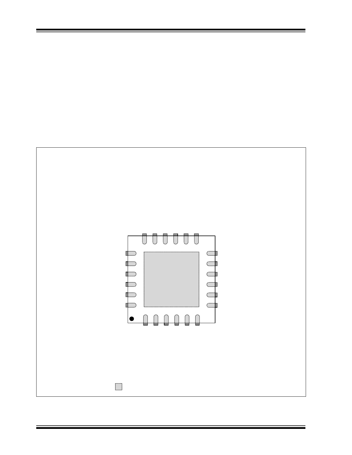
2.1
Pin Configuration
FIGURE 2-1:
USB2422 24-Pin SQFN
Thermal Slug
(must be connected to VSS)
12
11
10
9
8
7
USBDP_UP
19
XTALOUT/(CLKIN_EN)
20
XTALIN/CLKIN
21
RBIAS
24
23
PLLFILT
22
1
VD
D
3
3
2
US
B
D
P_
DN1
/PRT
_DIS_P1
3
US
B
D
M
_
DN
2
/P
R
T_
D
IS_
M
2
4
US
B
D
P_
DN2
/PRT
_DIS_P2
5
6
US
B
D
M
_
DN
1
/P
R
T_
D
IS_
M
1
NC
USBDM_UP
17
S
U
SP_I
N
D
/L
OCAL_
P
WR
/(NON_R
E
M
0
)
16
VB
U
S
_
D
E
T
RE
S
E
T
_
N
15
14
S
M
BC
L
K
/C
FG_
S
EL
0
VD
D
3
3
18
13
S
M
BD
A
T
A/NO
N
_
R
E
M1
Indicates pins on the bottom of the device.
OCS1_N
PRTPWR1/(BC_EN1)
VDD33
CRFILT
PRTPWR2
OCS2_N
USB2422
(Top View SQFN-24)
2013 - 2015 Microchip Technology Inc.
DS00001726B-page 7
USB2422
2.2
Pin Table
2.3
Pin Descriptions (Grouped by Function)
TABLE 2-1:
USB2422 PIN TABLE
UPSTREAM USB 2.0 INTERFACES (3 PINS)
USBDM_UP
usbDM_UP
VBUS_DET
DOWNSTREAM 2-PORT USB 2.0 INTERFACES (9 PINS)
USBDP_DN1/
PRT_DIS_P1
USBDM_DN1/
PRT_DIS_M1
USBDP_DN2/
PRT_DIS_P2
USBDM_DN2/
PRT_DIS_M2
PRTPWR1/
BC_EN1
PRTPWR2
OCS1_N
OCS2_N
RBIAS
SERIAL PORT INTERFACE (2 PINS)
SMBDATA/
NON_REM1
SMBCLK/
CFG_SEL
MISC (5 PINS)
XTALIN/
CLKIN
XTALOUT/
CLKIN_EN
RESET_N
SUSP_IND/
LOCAL_PWR/
NON_REM0
NC
POWER, GROUND, AND NO CONNECTS (5 PINS)
(3) VDD33
CRFILT
PLLFILT
VSS
TOTAL 24
TABLE 2-2:
USB2422 PIN DESCRIPTIONS
Pin #
Symbol
Buffer Type
Description
UPSTREAM USB 2.0 INTERFACES
19
20
USBDM_UP
USBDP_UP
IO-U
USB Bus Data:
Connect to the upstream USB bus data signals (host, port, or upstream
hub).
16
VBUS_DET
I
Detect Upstream VBUS Power:
Detects the state of upstream VBUS power. The hub monitors
VBUS_DET to determine when to assert the internal D+ pull-up resistor
(signalling a connect event)
When designing a detachable hub, this pin should be connected to
VBUS on the upstream port via a 2:1 voltage divider. Two 100 k
Ω
resistors are suggested.
For self-powered applications with a permanently attached host, this pin
must be connected to a dedicated host control output, or connected to
the 3.3 V domain that powers the host (typically VDD33).
USB2422
DS00001726B-page 8
2013 - 2015 Microchip Technology Inc.
DOWNSTREAM USB 2.0 INTERFACES
5
3
and
4
2
USBDP_DN[2:1]/
PRT_DIS_P[2:1]
and
USBDN_DN[2:1]/
PRT_DIS_M[2:1]
IO-U
Hi-Speed USB Data:
Connect to the downstream USB peripheral devices attached to the
hub’s ports.
Port Disable Strap Option:
If this strap is enabled by package and configuration settings (see
Table 4-1, "Hub Configuration Options"
), this pin will be sampled at
RESET_N negation to determine if the port is disabled.
Both USB data pins for the corresponding port must be tied to VDD33
to disable the associated downstream port.
7
PRTPWR1/
O12
USB Power Enable:
Enables power to USB peripheral devices that are downstream, where
the hub supports active high power controllers only.
BC_EN1
IPD
Battery Charging Strap Option:
Port 1 pin will be sampled at RESET_N negation to determine if port 1
supports the battery charging protocol (and thus the supporting external
port power controllers) that would enable a device to draw the currents
per the USB Battery Charging Specification.
This pin has an internal pull-down that will be removed after the strap
option hold time is completed.
BC_EN1= 1: Battery charging feature is supported for port 1
BC_EN1= 0: Battery charging feature is not supported for port 1
11
PRTPWR2
O12
USB Power Enable:
Enables power to USB peripheral devices that are downstream, where
the hub supports active high power controllers only.
8
12
OCS1_N
OCS2_N
IPU
Over-Current Sense:
Input from external current monitor indicating an over-current condition.
This pin contains an internal pull-up to the 3.3 V supply.
24
RBIAS
I-R
USB Transceiver Bias:
A12.0 k
Ω (+/- 1%) resistor is attached from ground to this pin to set the
transceiver’s internal bias settings.
SERIAL PORT INTERFACE
13
SMBDATA
I/OSD12
System Management Bus Data
NON_REM1
Non-removable Port Strap Option:
This pin is sampled (in conjunction with SUSP_IND/NON_REM0) at
RESET_N negation to determine if ports [2:1] contain permanently
attached (non-removable) devices:
NON_REM[1:0] = 00: all ports are removable
NON_REM[1:0] = 01: port 1 is non-removable
NON_REM[1:0] = 10: ports 1 and 2 are non-removable
NON_REM[1:0] = 11: reserved
See
Section 2.5, "Strap Pin Configuration"
for details.
14
SMBCLK/
I/OSD12
System Management Bus Clock
CFG_SEL
Configuration Select:
The logic state of this multifunction pin is internally latched on the rising
edge of RESET_N (RESET_N negation), and will determine the hub
configuration method as described in
Table 4-1
.
TABLE 2-2:
USB2422 PIN DESCRIPTIONS (CONTINUED)
Pin #
Symbol
Buffer Type
Description
2013 - 2015 Microchip Technology Inc.
DS00001726B-page 9
USB2422
MISC
22
XTALIN/
CLKIN
ICLKx
24 MHz Crystal or External Clock Input:
This pin connects to either one terminal of the crystal or to an external
24 MHz clock when a crystal is not used.
21
XTALOUT
OCLKx
Crystal Output:
This is the other terminal of the crystal circuit with 1.2 V p-p output and
a weak (< 1 mA) driving strength. When an external clock source is
used to drive XTALIN/CLKIN, leave this pin unconnected, or use with
appropriate caution.
15
RESET_N
IS
RESET Input:
The system must reset the chip by driving this input low. The minimum
active low pulse is 1
μs.
6
NC
IPD
Treat as a no connect pin or connect to ground. No trace or signal
should be routed or attached to this pin.
17
SUSP_IND
I/O12
Suspend Indicator:
Indicates the USB state of the hub.
negated : unconfigured, or configured and in USB Suspend
asserted : Hub is configured, and is active (i.e., not in suspend)
LOCAL_PWR
Local Power:
This input selects whether the hub reports itself as bus or self-powered
when dynamic power switching is enabled via the
Dynamic Power
Enable (DYNAMIC)
bit of the
Configuration Data Byte 2 Register
(CFG2)
. This pin is sampled at POR/Reset before the USB Hub Attach
command is sent. Once the hub has entered the attach state (as
indicated by the
USB Attach and Write Protect (USB_ATTACH)
bit of the
Status/Command Register (STCD)
), this pin cannot be changed.
Low : self/local power source is not available (i.e., the Hub gets all
power from the upstream USB VBus).
High : self/local power source is available.
Note:
Never tie this pin directly to VDD33, as doing so may cause it
to act as SUSP_IND.
Note:
This pin assumes the meaning of local power input only if
properly configured via SMBus. If the hub is configured via
straps, it is NON_REM0 at reset and SUSP_IND after reset.
(NON_REM0)
Non-Removable Port Strap Option:
This pin is sampled (in conjunction with SUSP_IND/NON_REM0) at
RESET_N negation to determine if ports [2:1] contain permanently
attached (non-removable) devices:
NON_REM[1:0] = 00: all ports are removable
NON_REM[1:0] = 01: port 1 is non-removable
NON_REM[1:0] = 10: ports 1 and 2 are non-removable
NON_REM[1:0] = 11: reserved
See
Section 2.5, "Strap Pin Configuration"
for details.
TABLE 2-2:
USB2422 PIN DESCRIPTIONS (CONTINUED)
Pin #
Symbol
Buffer Type
Description
USB2422
DS00001726B-page 10
2013 - 2015 Microchip Technology Inc.
2.4
Buffer Type Descriptions
2.5
Strap Pin Configuration
If a pin's strap function is enabled through hub configuration selection (
Table 4-1
), the strap pins must be pulled either
high or low using the values provided in
Table 2-4
. Each strap option is dependent on the pin’s buffer type, as outlined
in the sections that follow.
POWER, GROUND, and NO CONNECTS
1
9
18
VDD33
3.3 V power to the chip.
A 1.0
μF low-ESR capacitor to VSS is required on pin 9 as close as
possible to the pin. A 0.1
μF low-ESR capacitor to VSS is required on
pin 1 as close as possible to the pin.
10
CRFILT
VDD Core Regulator Filter Capacitor:
This pin requires a 1.0
μF low-ESR capacitor to VSS for proper
operation.
23
PLLFILT
PLL Regulator Filter Capacitor:
This pin can have up to a 0.1
μF low-ESR capacitor to VSS, or be left
unconnected.
VSS
Ground Pad/ePad:
The package slug is the only VSS for the device and must be tied to
ground with multiple vias.
TABLE 2-3:
BUFFER TYPE DESCRIPTIONS
Buffer
Description
I/O
Input/Output
IPD
Input with internal weak pull-down resistor
IPU
Input with internal weak pull-up resistor
IS
Input with Schmitt trigger
I/O12
Input/Output buffer with 12 mA sink and 12 mA source
ICLKx
XTAL clock input
OCLKx
XTAL clock output
I-R
RBIAS
I/O-U
Analog Input/Output defined in USB specification
TABLE 2-4:
STRAP OPTION SUMMARY
Strap Option
Resistor Value
Buffer Type
Notes
Non-Removable
47 - 100 k
Ω
I/O
Internal Pull-Down (IPD)
10 k
Ω
IPD
• Only applicable to port power pins
• Contains a built-in resistor
LED
47 - 100 k
Ω
I/O
TABLE 2-2:
USB2422 PIN DESCRIPTIONS (CONTINUED)
Pin #
Symbol
Buffer Type
Description
2013 - 2015 Microchip Technology Inc.
DS00001726B-page 1
General Description
The Microchip USB2422 hub is a low-power, single
transaction translator, hub controller IC with two down-
stream ports for embedded USB solutions. The hub
controller can attach to an upstream port as a Hi-Speed
and Full-Speed hub or as a Full-Speed only hub. The
hub supports Low-Speed, Full-Speed, and Hi-Speed
(when configured as a Hi-Speed hub) downstream
devices on the enabled downstream ports.
All required resistors on the USB ports are integrated
into the hub. This includes all series termination resis-
tors on D+ and D- pins and all required pull-down and
pull-up resistors on D+ and D- pins. The over-current
sense inputs for the downstream facing ports have
internal pull-up resistors.
Features
• Supports the USB Battery Charging Specification,
Revision 1.1
• Fully integrated USB termination and pull-up/pull-
down resistors
• Supports a single external 3.3 V supply source;
internal regulators provide 1.2 V internal core volt-
age
• On-chip driver for 24 MHz crystal resonator or
external 24 MHz clock input
• ESD protection up to 6 kV on all USB pins
• Supports self-powered operation
• The hub contains a built-in default configuration;
no external configuration options or components
are required
• Downstream ports as non-removable ports
• Downstream port power control and over-current
detection on an individual or ganged basis
• Supports compound devices on a port-by-port
basis
• 24-pin SQFN (4x4 mm), RoHS-compliant pack-
age
• Commercial temperature range support:
0ºC to +70ºC
• Industrial temperature range support:
-40ºC to +85ºC
Highlights
• High performance, low-power, small footprint hub
controller IC with two downstream ports
• Fully compliant with the USB 2.0 Specification
• Optimized for minimal bill-of-materials and low-
cost designs
Applications
• LCD monitors and TVs
• Multi-function USB peripherals
• PC motherboards
• Set-top boxes, DVD players, DVR/PVR
• Printers and scanners
• PC media drive bay
• Portable hub boxes
• Mobile PC docking
• Embedded systems
• Gaming consoles
• Cable/DSL modems
• HDD enclosures
• KVM switches
• Server front panels
• Point-of-Sale (POS) systems
• IP telephony
• Automobile/home audio systems
• Thin client terminals
USB2422
2-Port USB 2.0 Hi-Speed Hub Controller
USB2422
DS00001726B-page 2
2013 - 2015 Microchip Technology Inc.
TO OUR VALUED CUSTOMERS
It is our intention to provide our valued customers with the best documentation possible to ensure successful use of your Microchip
products. To this end, we will continue to improve our publications to better suit your needs. Our publications will be refined and
enhanced as new volumes and updates are introduced.
If you have any questions or comments regarding this publication, please contact the Marketing Communications Department via
E-mail at
docerrors@microchip.com
. We welcome your feedback.
Most Current Data Sheet
To obtain the most up-to-date version of this data sheet, please register at our Worldwide Web site at:
http://www.microchip.com
You can determine the version of a data sheet by examining its literature number found on the bottom outside corner of any page.
The last character of the literature number is the version number, (e.g., DS30000000A is version A of document DS30000000).
Errata
An errata sheet, describing minor operational differences from the data sheet and recommended workarounds, may exist for cur-
rent devices. As device/documentation issues become known to us, we will publish an errata sheet. The errata will specify the
revision of silicon and revision of document to which it applies.
To determine if an errata sheet exists for a particular device, please check with one of the following:
• Microchip’s Worldwide Web site;
http://www.microchip.com
• Your local Microchip sales office (see last page)
When contacting a sales office, please specify which device, revision of silicon and data sheet (include -literature number) you are
using.
Customer Notification System
Register on our web site at
www.microchip.com
to receive the most current information on all of our products.
2013 - 2015 Microchip Technology Inc.
DS00001726B-page 3
USB2422
Table of Contents
1.0 Block Diagram ................................................................................................................................................................................. 4
2.0 Pin Descriptions .............................................................................................................................................................................. 6
3.0 Battery Charging Support ............................................................................................................................................................. 14
4.0 Configuration Options ................................................................................................................................................................... 16
5.0 DC Parameters ............................................................................................................................................................................. 35
6.0 AC Specifications .......................................................................................................................................................................... 38
7.0 Package Outline ............................................................................................................................................................................ 40
Appendix A: Acronyms ........................................................................................................................................................................ 41
Appendix B: References ..................................................................................................................................................................... 42
Appendix C: Data Sheet Revision History .......................................................................................................................................... 43
The Microchip Web Site ...................................................................................................................................................................... 44
Customer Change Notification Service ............................................................................................................................................... 44
Customer Support ............................................................................................................................................................................... 44
Product Identification System ............................................................................................................................................................. 45
USB2422
DS00001726B-page 4
2013 - 2015 Microchip Technology Inc.
1.0
BLOCK DIAGRAM
FIGURE 1-1:
USB2422 BLOCK DIAGRAM
To Upstream
V
BUS
3.3V
Upstream
PHY
Upstream USB
Data
Repeater
Controller
SIE
Serial
Interface
PLL
24 MHz Crystal
To
SMBus Master
Routing & Port Re-Ordering
Logic
SMBCLK
SMBDATA
Port
Controller
Bus-Power
Detect/V
BUS
Pulse
TT
PHY#1
Port #1
OC
Sense
Switch
Driver
PHY#2
Port #2
OC
Sense
Switch
Driver
USB Data
Downstream
OC Sense
Switch
USB Data
Downstream
OC Sense
Switch
CRFILT PLLFILT
1.2V Reg
2013 - 2015 Microchip Technology Inc.
DS00001726B-page 5
USB2422
Within this manual, the following abbreviations and symbols are used to improve readability.
Example
Description
BIT
Name of a single bit within a field
FIELD.BIT
Name of a single bit (BIT) in FIELD
x…y
Range from x to y, inclusive
BITS[m:n]
Groups of bits from m to n, inclusive
PIN
Pin Name
zzzzb
Binary number (value zzzz)
0xzzz
Hexadecimal number (value zzz)
zzh
Hexadecimal number (value zz)
rsvd
Reserved memory location. Must write 0, read value indeterminate
code
Instruction code, or API function or parameter
Multi Word Name
Used for multiple words that are considered a single unit, such as:
Resource Allocate message, or Connection Label, or Decrement Stack Pointer
instruction.
Section Name
Section or Document name.
x
Don’t care
<Parameter>
<> indicate a Parameter is optional or is only used under some
conditions
{,Parameter}
Braces indicate Parameter(s) that repeat one or more times.
[Parameter]
Brackets indicate a nested Parameter. This Parameter is not real and
actually decodes into one or more real parameters.
USB2422
DS00001726B-page 6
2013 - 2015 Microchip Technology Inc.
2.0
PIN DESCRIPTIONS
This chapter is organized by a set of pin configurations followed by a corresponding pin list organized by function
according to their associated interface. A detailed description list of each signal (named in the pin list) is organized by
function in
Table 2-2, “USB2422 Pin Descriptions,” on page 7
. Refer to
Table 2-3, “Buffer Type Descriptions,” on page 10
for a list of buffer types.
An N at the end of a signal name indicates that the active (asserted) state occurs when the signal is at a low voltage
level. When the N is not present, the signal is asserted when it is at a high voltage level. The terms assertion and nega-
tion are used exclusively in order to avoid confusion when working with a mixture of active low and active high signals.
The term assert, or assertion, indicates that a signal is active, independent of whether that level is represented by a high
or low voltage. The term negate, or negation, indicates that a signal is inactive.
2.1
Pin Configuration
FIGURE 2-1:
USB2422 24-Pin SQFN
Thermal Slug
(must be connected to VSS)
12
11
10
9
8
7
USBDP_UP
19
XTALOUT/(CLKIN_EN)
20
XTALIN/CLKIN
21
RBIAS
24
23
PLLFILT
22
1
VD
D
3
3
2
US
B
D
P_
DN1
/PRT
_DIS_P1
3
US
B
D
M
_
DN
2
/P
R
T_
D
IS_
M
2
4
US
B
D
P_
DN2
/PRT
_DIS_P2
5
6
US
B
D
M
_
DN
1
/P
R
T_
D
IS_
M
1
NC
USBDM_UP
17
S
U
SP_I
N
D
/L
OCAL_
P
WR
/(NON_R
E
M
0
)
16
VB
U
S
_
D
E
T
RE
S
E
T
_
N
15
14
S
M
BC
L
K
/C
FG_
S
EL
0
VD
D
3
3
18
13
S
M
BD
A
T
A/NO
N
_
R
E
M1
Indicates pins on the bottom of the device.
OCS1_N
PRTPWR1/(BC_EN1)
VDD33
CRFILT
PRTPWR2
OCS2_N
USB2422
(Top View SQFN-24)
2013 - 2015 Microchip Technology Inc.
DS00001726B-page 7
USB2422
2.2
Pin Table
2.3
Pin Descriptions (Grouped by Function)
TABLE 2-1:
USB2422 PIN TABLE
UPSTREAM USB 2.0 INTERFACES (3 PINS)
USBDM_UP
usbDM_UP
VBUS_DET
DOWNSTREAM 2-PORT USB 2.0 INTERFACES (9 PINS)
USBDP_DN1/
PRT_DIS_P1
USBDM_DN1/
PRT_DIS_M1
USBDP_DN2/
PRT_DIS_P2
USBDM_DN2/
PRT_DIS_M2
PRTPWR1/
BC_EN1
PRTPWR2
OCS1_N
OCS2_N
RBIAS
SERIAL PORT INTERFACE (2 PINS)
SMBDATA/
NON_REM1
SMBCLK/
CFG_SEL
MISC (5 PINS)
XTALIN/
CLKIN
XTALOUT/
CLKIN_EN
RESET_N
SUSP_IND/
LOCAL_PWR/
NON_REM0
NC
POWER, GROUND, AND NO CONNECTS (5 PINS)
(3) VDD33
CRFILT
PLLFILT
VSS
TOTAL 24
TABLE 2-2:
USB2422 PIN DESCRIPTIONS
Pin #
Symbol
Buffer Type
Description
UPSTREAM USB 2.0 INTERFACES
19
20
USBDM_UP
USBDP_UP
IO-U
USB Bus Data:
Connect to the upstream USB bus data signals (host, port, or upstream
hub).
16
VBUS_DET
I
Detect Upstream VBUS Power:
Detects the state of upstream VBUS power. The hub monitors
VBUS_DET to determine when to assert the internal D+ pull-up resistor
(signalling a connect event)
When designing a detachable hub, this pin should be connected to
VBUS on the upstream port via a 2:1 voltage divider. Two 100 k
Ω
resistors are suggested.
For self-powered applications with a permanently attached host, this pin
must be connected to a dedicated host control output, or connected to
the 3.3 V domain that powers the host (typically VDD33).
USB2422
DS00001726B-page 8
2013 - 2015 Microchip Technology Inc.
DOWNSTREAM USB 2.0 INTERFACES
5
3
and
4
2
USBDP_DN[2:1]/
PRT_DIS_P[2:1]
and
USBDN_DN[2:1]/
PRT_DIS_M[2:1]
IO-U
Hi-Speed USB Data:
Connect to the downstream USB peripheral devices attached to the
hub’s ports.
Port Disable Strap Option:
If this strap is enabled by package and configuration settings (see
Table 4-1, "Hub Configuration Options"
), this pin will be sampled at
RESET_N negation to determine if the port is disabled.
Both USB data pins for the corresponding port must be tied to VDD33
to disable the associated downstream port.
7
PRTPWR1/
O12
USB Power Enable:
Enables power to USB peripheral devices that are downstream, where
the hub supports active high power controllers only.
BC_EN1
IPD
Battery Charging Strap Option:
Port 1 pin will be sampled at RESET_N negation to determine if port 1
supports the battery charging protocol (and thus the supporting external
port power controllers) that would enable a device to draw the currents
per the USB Battery Charging Specification.
This pin has an internal pull-down that will be removed after the strap
option hold time is completed.
BC_EN1= 1: Battery charging feature is supported for port 1
BC_EN1= 0: Battery charging feature is not supported for port 1
11
PRTPWR2
O12
USB Power Enable:
Enables power to USB peripheral devices that are downstream, where
the hub supports active high power controllers only.
8
12
OCS1_N
OCS2_N
IPU
Over-Current Sense:
Input from external current monitor indicating an over-current condition.
This pin contains an internal pull-up to the 3.3 V supply.
24
RBIAS
I-R
USB Transceiver Bias:
A12.0 k
Ω (+/- 1%) resistor is attached from ground to this pin to set the
transceiver’s internal bias settings.
SERIAL PORT INTERFACE
13
SMBDATA
I/OSD12
System Management Bus Data
NON_REM1
Non-removable Port Strap Option:
This pin is sampled (in conjunction with SUSP_IND/NON_REM0) at
RESET_N negation to determine if ports [2:1] contain permanently
attached (non-removable) devices:
NON_REM[1:0] = 00: all ports are removable
NON_REM[1:0] = 01: port 1 is non-removable
NON_REM[1:0] = 10: ports 1 and 2 are non-removable
NON_REM[1:0] = 11: reserved
See
Section 2.5, "Strap Pin Configuration"
for details.
14
SMBCLK/
I/OSD12
System Management Bus Clock
CFG_SEL
Configuration Select:
The logic state of this multifunction pin is internally latched on the rising
edge of RESET_N (RESET_N negation), and will determine the hub
configuration method as described in
Table 4-1
.
TABLE 2-2:
USB2422 PIN DESCRIPTIONS (CONTINUED)
Pin #
Symbol
Buffer Type
Description
2013 - 2015 Microchip Technology Inc.
DS00001726B-page 9
USB2422
MISC
22
XTALIN/
CLKIN
ICLKx
24 MHz Crystal or External Clock Input:
This pin connects to either one terminal of the crystal or to an external
24 MHz clock when a crystal is not used.
21
XTALOUT
OCLKx
Crystal Output:
This is the other terminal of the crystal circuit with 1.2 V p-p output and
a weak (< 1 mA) driving strength. When an external clock source is
used to drive XTALIN/CLKIN, leave this pin unconnected, or use with
appropriate caution.
15
RESET_N
IS
RESET Input:
The system must reset the chip by driving this input low. The minimum
active low pulse is 1
μs.
6
NC
IPD
Treat as a no connect pin or connect to ground. No trace or signal
should be routed or attached to this pin.
17
SUSP_IND
I/O12
Suspend Indicator:
Indicates the USB state of the hub.
negated : unconfigured, or configured and in USB Suspend
asserted : Hub is configured, and is active (i.e., not in suspend)
LOCAL_PWR
Local Power:
This input selects whether the hub reports itself as bus or self-powered
when dynamic power switching is enabled via the
Dynamic Power
Enable (DYNAMIC)
bit of the
Configuration Data Byte 2 Register
(CFG2)
. This pin is sampled at POR/Reset before the USB Hub Attach
command is sent. Once the hub has entered the attach state (as
indicated by the
USB Attach and Write Protect (USB_ATTACH)
bit of the
Status/Command Register (STCD)
), this pin cannot be changed.
Low : self/local power source is not available (i.e., the Hub gets all
power from the upstream USB VBus).
High : self/local power source is available.
Note:
Never tie this pin directly to VDD33, as doing so may cause it
to act as SUSP_IND.
Note:
This pin assumes the meaning of local power input only if
properly configured via SMBus. If the hub is configured via
straps, it is NON_REM0 at reset and SUSP_IND after reset.
(NON_REM0)
Non-Removable Port Strap Option:
This pin is sampled (in conjunction with SUSP_IND/NON_REM0) at
RESET_N negation to determine if ports [2:1] contain permanently
attached (non-removable) devices:
NON_REM[1:0] = 00: all ports are removable
NON_REM[1:0] = 01: port 1 is non-removable
NON_REM[1:0] = 10: ports 1 and 2 are non-removable
NON_REM[1:0] = 11: reserved
See
Section 2.5, "Strap Pin Configuration"
for details.
TABLE 2-2:
USB2422 PIN DESCRIPTIONS (CONTINUED)
Pin #
Symbol
Buffer Type
Description
USB2422
DS00001726B-page 10
2013 - 2015 Microchip Technology Inc.
2.4
Buffer Type Descriptions
2.5
Strap Pin Configuration
If a pin's strap function is enabled through hub configuration selection (
Table 4-1
), the strap pins must be pulled either
high or low using the values provided in
Table 2-4
. Each strap option is dependent on the pin’s buffer type, as outlined
in the sections that follow.
POWER, GROUND, and NO CONNECTS
1
9
18
VDD33
3.3 V power to the chip.
A 1.0
μF low-ESR capacitor to VSS is required on pin 9 as close as
possible to the pin. A 0.1
μF low-ESR capacitor to VSS is required on
pin 1 as close as possible to the pin.
10
CRFILT
VDD Core Regulator Filter Capacitor:
This pin requires a 1.0
μF low-ESR capacitor to VSS for proper
operation.
23
PLLFILT
PLL Regulator Filter Capacitor:
This pin can have up to a 0.1
μF low-ESR capacitor to VSS, or be left
unconnected.
VSS
Ground Pad/ePad:
The package slug is the only VSS for the device and must be tied to
ground with multiple vias.
TABLE 2-3:
BUFFER TYPE DESCRIPTIONS
Buffer
Description
I/O
Input/Output
IPD
Input with internal weak pull-down resistor
IPU
Input with internal weak pull-up resistor
IS
Input with Schmitt trigger
I/O12
Input/Output buffer with 12 mA sink and 12 mA source
ICLKx
XTAL clock input
OCLKx
XTAL clock output
I-R
RBIAS
I/O-U
Analog Input/Output defined in USB specification
TABLE 2-4:
STRAP OPTION SUMMARY
Strap Option
Resistor Value
Buffer Type
Notes
Non-Removable
47 - 100 k
Ω
I/O
Internal Pull-Down (IPD)
10 k
Ω
IPD
• Only applicable to port power pins
• Contains a built-in resistor
LED
47 - 100 k
Ω
I/O
TABLE 2-2:
USB2422 PIN DESCRIPTIONS (CONTINUED)
Pin #
Symbol
Buffer Type
Description