

2009 - 2015 Microchip Technology Inc.
DS00002005A-page 1
General Description
The Microchip USB2250/50i/51/51i is a USB 2.0 com-
pliant, Hi-Speed mass storage class peripheral control-
ler intended for reading and writing to more than 24
popular flash media formats from the CompactFlash
®
(CF), SmartMedia
TM
(SM), xD-Picture Card
TM
(xD)
1
,
Memory Stick
®
(MS), Secure Digital (SD), and MultiMe-
diaCard
TM
(MMC) families.
The USB2250/50i/51/51i is a fully integrated, single
chip solution capable of ultra high performance opera-
tion. Average sustained transfer rates exceeding 35
MB/s are possible if the media and host can support
those rates.
Highlights
• 128-pin VTQFP (14x14 mm) RoHS compliant
package
• Targeted for applications in which single or
"combo" media sockets are used
• Supports multiple simultaneous card insertions
• Flexible assignment of number of LUNs and how
card types are associated with the LUNs
• Hardware-controlled data flow architecture for all
self-mapped media
• Pipelined hardware support for access to non-
self-mapped media
• Order number with “i” denotes the version that
supports the industrial temperature range of -40ºC
to 85ºC
Hardware Features
• Single chip flash media controller with non-multi-
plexed interface for independent card sockets
• Flash Media Specification Revision Compliance
- CompactFlash 4.1
- Secure Digital 2.0
- MultiMediaCard 4.2
• MMC Streaming Mode support
- Memory Stick 1.43
- Memory Stick Pro Format 1.02
- Memory Stick Duo Format 1.10
- Memory Stick Pro-HG Duo Format 1.01
- xD-Picture Card 1.2
- SmartMedia 1.3
• Extended configuration options
- xD player mode operation
- Socket switch polarities, etc.
• Media Activity LED
• On board 24 MHz crystal driver circuit
• Optional external 24 MHz clock input
- 4 Independent internal card power FETs
- 200 mA each
- "Fold-back" short circuit protection
• 8051 8-bit microprocessor
- 60 MHz - single cycle execution
- 64 KB ROM | 14 KB RAM
• Internal regulator for 1.8 V core operation
• Optimized pinout improves signal routing which
eases implementation for improved signal integ-
rity
OEM Selectable
• Vendor, product, and language IDs
• Manufacturer ID and product strings (28 charac-
ter)
• Serial number string (12h digit max)
• Customizable vendor specific data by optional
use of external serial EEPROM
• Bus- or self-powered selection
• LED blink interval or duration
• Internal power FET configuration
Software Features
• Optimized for low latency interrupt handling
• Reduced memory footprint
• Device Firmware Upgrade (DFU) support of exter-
nal EEPROM or External Flash
- Assembly line support
- End user field upgrade support
- DFU Package consists of driver, firmware,
sample DFU application and source code,
DFU driver API
• Optional custom firmware with up to 128 KB
external ROM
Applications
• Flash Media Card Reader/Writer
• Printers
• Desktop and Mobile PCs
• Consumer A/V
• Media Players/Viewers
• Vista ReadyBoost
TM
1.) xD-Picture Card not applicable to USB2251.
USB2250/50i/51/51i
Ultra Fast USB 2.0 Multi-Slot Flash Media Controller

USB2250/50i/51/51i
DS00002005A-page 2
2009 - 2015 Microchip Technology Inc.
TO OUR VALUED CUSTOMERS
It is our intention to provide our valued customers with the best documentation possible to ensure successful use of your Microchip
products. To this end, we will continue to improve our publications to better suit your needs. Our publications will be refined and
enhanced as new volumes and updates are introduced.
If you have any questions or comments regarding this publication, please contact the Marketing Communications Department via
E-mail at
docerrors@microchip.com
. We welcome your feedback.
Most Current Data Sheet
To obtain the most up-to-date version of this data sheet, please register at our Worldwide Web site at:
http://www.microchip.com
You can determine the version of a data sheet by examining its literature number found on the bottom outside corner of any page.
The last character of the literature number is the version number, (e.g., DS30000000A is version A of document DS30000000).
Errata
An errata sheet, describing minor operational differences from the data sheet and recommended workarounds, may exist for cur-
rent devices. As device/documentation issues become known to us, we will publish an errata sheet. The errata will specify the
revision of silicon and revision of document to which it applies.
To determine if an errata sheet exists for a particular device, please check with one of the following:
• Microchip’s Worldwide Web site;
http://www.microchip.com
• Your local Microchip sales office (see last page)
When contacting a sales office, please specify which device, revision of silicon and data sheet (include -literature number) you are
using.
Customer Notification System
Register on our web site at
www.microchip.com
to receive the most current information on all of our products.

2009 - 2015 Microchip Technology Inc.
DS00002005A-page 3
USB2250/50i/51/51i
Table of Contents
1.0 Introduction ..................................................................................................................................................................................... 4
2.0 Pin Configuration ............................................................................................................................................................................ 6
3.0 Block Diagram ................................................................................................................................................................................. 7
4.0 Pin Table ......................................................................................................................................................................................... 8
5.0 Pin Descriptions ............................................................................................................................................................................ 10
6.0 Pin Reset State Table ................................................................................................................................................................... 17
7.0 Configuration Options ................................................................................................................................................................... 21
8.0 AC Specifications .......................................................................................................................................................................... 32
9.0 DC Parameters ............................................................................................................................................................................. 34
10.0 Package Outline .......................................................................................................................................................................... 38
Appendix A: Data Sheet Revision History ........................................................................................................................................... 39
Product Identification System ............................................................................................................................................................. 40
The Microchip Web Site ...................................................................................................................................................................... 41
Customer Change Notification Service ............................................................................................................................................... 41
Customer Support ............................................................................................................................................................................... 41

2009 - 2015 Microchip Technology Inc.
DS00002005A-page 4
USB2250/50i/51/51i
1.0
INTRODUCTION
The Microchip USB2250/50i/51/51i is a flash media card reader solution fully compliant with the USB 2.0 specification.
All required resistors on the USB ports are integrated into the device. This includes all series termination resistors on
D+ and D– pins and all required pull-down and pull-up resistors. The over-current sense inputs for the downstream fac-
ing ports have internal pull-up resistors.
Hardware Features
• Single chip flash media controller
• USB2250/USB2251 supports the commercial temperature range of 0°C to +70°C
• USB2250i/USB2251i supports the industrial temperature range of -40°C to +85°C
• 8051 8-bit microprocessor
- 60 MHz - single cycle execution
- 64 KB ROM |14 KB RAM
• Integrated regulator for 1.8 V core operation
• Flash Media Card Specification Revision Compliance
• Compact Flash 4.1
- CF UDMA Modes 0-4
- CF PIO Modes 0-6
• Secure Digital 2.0
- HS-SD and HC-SD
- TransFlash™ and reduced form factor media
• MultiMediaCard 4.2
- 1/4/8 bit MMC
• Memory Stick 1.43
• Memory Stick Pro Format 1.02
• Memory Stick Pro-HG Duo Format 1.01
- Memory Stick, MS Duo, HS-MS, MS Pro-HG, MS Pro
• Memory Stick Duo 1.10
• Smart Media 1.3
• xD-Picture Card 1.2
Software Features
• If the OEM is using an external EEPROM, the following features are available:
- Customizable vendor, product, and device ID’s
- 12-hex digits maximum for the serial number string
- 28-character manufacturer ID and product strings for the flash media reader/writer

USB2250/50i/51/51i
DS00002005A-page 5
2009 - 2015 Microchip Technology Inc.
1.1
Acronyms
ATA:
Advanced Technology Attachment
CFC:
Compact Flash Controller
FET:
Field Effect Transistor
LUN:
Logical Unit Number
MMC: MultiMediaCard
MSC:
Memory Stick Controller
PLL: Phase-Locked
Loop
RoHS:
Restriction of Hazardous Substances Directive
RXD:
Received eXchange Data
SDC: Secure
Digital
Controller
SIE:
Serial Interface Engine
SMC:
SmartMedia Controller
True IDE Mode: True Integrated Drive Electronics Mode
TXD:
Transmit eXchange Data
UART: Universal
Asynchronous
Receiver-Transmitter
UCHAR: Unsigned
Character
UINT:
Unsigned Integer
VTQFP:
Very Thin Quad Flat Package
2009 - 2015 Microchip Technology Inc.
DS00002005A-page 6
USB2250/50i/51/51i
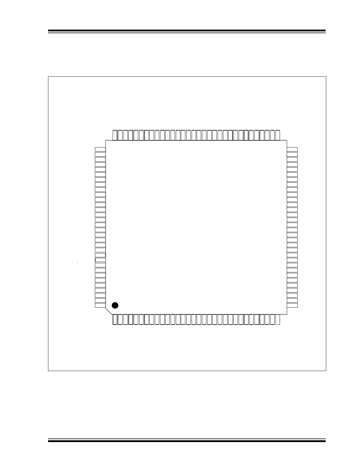
2.0
PIN CONFIGURATION
FIGURE 2-1:
128-PIN VTQFP DIAGRAM
97
MS_D6
99
MS_D3
100
MS_D7
101
MS_SCLK
102
VSS
103
TEST
104
VDD33
106
MA7
107
MA13
108
MA6
109
MA8
110
MA5
111
MA9
112
MA4
113
MA11
114
MA3
115
nMRD
116
MA2
117
CF_DMARQ / RXD
SCL / xD_ID
CF_DMACK
120
LED
121
VBUS_DET
122
VSS
123
XTAL2
124
XTAL1 (CLKIN)
125
VDD18PLL
126
VSS
127
RBIAS
128
VDD33
64
nRESET
63
CF_D5
62
CF_D12
61
CF_D4
60
CF_D11
59
CF_D3
58
CF_nCD
57
SM_nCD
56
SM_nB/R
55
SM_nRE
54
SM_nCE
53
SM_CLE
52
SM_ALE
51
VSS
50
VDD33
49
VDD18
48
SM_nWE
47
SM_nWP
46
SM_D0
45
SM_D1
44
SM_D2
43
SM_D3
42
SM_D4
41
SM_D5
40
SM_D6
39
SM_D7
38
SM_nWPS
37
MD0
36
MD1
35
MD2
34
MD3
33
MD7
96
MS
_
D
2
95
MS
_
D
4
94
M
S
_D0 /
MS
_
S
DIO
93
MS
_
D
5
92
MS
_
D
1
91
MS
_
B
S
90
CF
_D10
89
CF
_D9
88
CF
_D2
87
CF
_D8
86
CF
_D1
85
CF
_D0
84
CF
_SA0
83
CF
_SA1
82
CF
_SA2
81
VS
S
80
CF
_IORDY
79
CF
_nRESET
78
CR
D_PW
R1
77
V
DD33
76
CR
D_PW
R2
75
VS
S
74
CF
_IRQ
73
CF
_nIOW
72
CF
_nIOR
71
CF
_nCS0
70
CF
_D15
69
CF
_D7
68
CF
_D14
67
CF
_D6
66
CF
_D13
65
V
DD33
USB225X
128 VTQFP
(Top View)
1
MA12
2
MA15
3
nM
WR
4
MA14
5
SD
A
6
REG_EN
7
USB+
8
US
B-
9
VSS
10
SD_
D
1
11
SD_
D
6
12
SD_
D
0
13
SD_
D
7
15
VDD33
16
17
VSS
18
SD_CLK
19
SD_
D
5
20
SD_
C
MD
21
SD_
D
4
22
SD_
D
3
23
SD_
D
2
24
MA10
25
MA1 /
CL
K_S
E
L1
26
nMCE
27
MA0 /
CL
K_S
E
L0
28
MA16
29
MD
6
30
MD
5
31
MD
4
SD
_n
CD
14
CRD
_PWR
0
118
CRD
_PWR
3
119
32
98
MS_INS
105
SD_WP
2009 - 2015 Microchip Technology Inc.
DS00002005A-page 7
USB2250/50i/51/51i
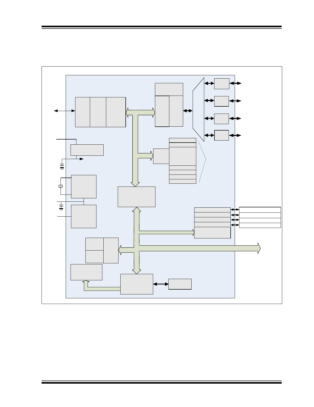
3.0
BLOCK DIAGRAM
FIGURE 3-1:
USB2250/50I/51/51I BLOCK DIAGRAM
FMDU
CTL
8051
PROCESSOR
SFR
RAM
CF/
GPIO (16)
MS
SM
RAM
USB
Host
AUTO_CBW
PROC
PHY
FMI
XDATA BRIDGE
+ BUS ARBITER
BUS
INTFC
BUS
INTFC
BUS
INTFC
EP0 TX
EP0 RX
EP2 TX
EP2 RX
EP1 RX
EP1 TX
ROM
64 KB
RAM
10 KB
ADDR
MAP
PWR_FET1
PWR_FET3
CRD_PWR0
CRD_PWR1
CRD_PWR3
Clock
Generation and
Control
CRD_PWR2
SD/
MMC
4K
total
PWR_FET0
PWR_FET2
GPIOs
Program Memory I/O Bus
3.3 V
1.8 V Reg
VDD18
3.3 V
VDD18PLL
PLL
24 MHz
Crystal
SIE
CTL
1.8 V Reg
USB2250 / USB2251

2009 - 2015 Microchip Technology Inc.
DS00002005A-page 8
USB2250/50i/51/51i
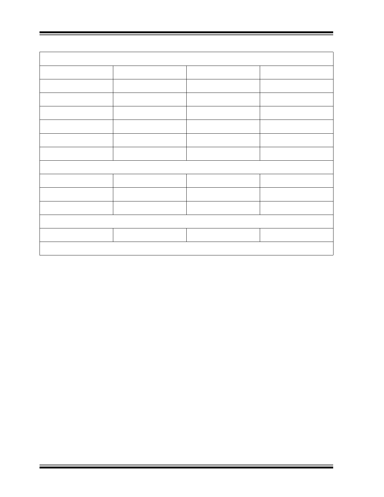
4.0
PIN TABLE
4.1
128-Pin Package
TABLE 4-1:
128-PIN VTQFP PACKAGE
COMPACT FLASH INTERFACE (28 PINS)
CF_D0
CF_D1
CF_D2
CF_D3
CF_D4
CF_D5
CF_D6
CF_D7
CF_D8
CF_D9
CF_D10
CF_D11
CF_D12
CF_D13
CF_D14
CF_D15
CF_nIOR
CF_nIOW
CF_IRQ
CF_nRESET
CF_IORDY
CF_nCS0
CF_DMACK
CF_SA0
CF_SA1
CF_SA2
CF_nCD
CF_DMARQ
SMARTMEDIA INTERFACE (17 PINS)
SM_D0
SM_D1
SM_D2
SM_D3
SM_D4
SM_D5
SM_D6
SM_D7
SM_ALE
SM_CLE
SM_nRE
SM_nWE
SM_nWP
SM_nB/R
SM_nCE
SM_nCD
SM_nWPS
MEMORY STICK INTERFACE (11 PINS)
MS_BS
MS_D0 / MS_SDIO
MS_SCLK
MS_INS
MS_D1
MS_D2
MS_D3
MS_D4
MS_D5
MS_D6
MS_D7
SECURE DIGITAL / MULTIMEDIACARD INTERFACE (12 PINS)
SD_CMD
SD_CLK
SD_D0
SD_D1
SD_D2
SD_D3
SD_WP
SD_nCD
SD_D4
SD_D5
SD_D6
SD_D7
USB INTERFACE (6 PINS)
USB+
USB-
RBIAS
XTAL2
XTAL1 (CLKIN)
REG_EN
USB2250/50i/51/51i
DS00002005A-page 9
2009 - 2015 Microchip Technology Inc.
MEMORY/IO INTERFACE (28 PINS)
MA0 / CLK_SEL0
MA1 / CLK_SEL1
MA2
MA3
MA4
MA5
MA6
MA7
MA8
MA9
MA10
MA11
MA12
MA13
MA14
MA15
MA16
MD0
MD1
MD2
MD3
MD4
MD5
MD6
MD7
nMRD
nMWR
nMCE
MISC (10 PINS)
nRESET
VBUS_DET
SCL / xD_ID
SDA
LED
CRD_PWR0
CRD_PWR1
CRD_PWR2
CRD_PWR3
TEST
DIGITAL, POWER (16 PINS)
(6) VDD33
(8) VSS
VDD18
VDD18PLL
TOTAL 128
TABLE 4-1:
128-PIN VTQFP PACKAGE (CONTINUED)

2009 - 2015 Microchip Technology Inc.
DS00002005A-page 10
USB2250/50i/51/51i
5.0
PIN DESCRIPTIONS
This section provides a detailed description of each signal. The signals are arranged in functional groups according to
their associated interface. The pin descriptions are applied when using the internal default firmware and can be refer-
enced in
Section 7.0, "Configuration Options," on page 21
. Please reference
Section 1.1, "Acronyms," on page 5
for a
list of the acronyms used.
The “n” symbol in the signal name indicates that the active, or asserted, state occurs when the signal is at a low voltage
level. When “n” is not present in the signal name, the signal is asserted at the high voltage level.
The terms assertion and negation are used exclusively. This is done to avoid confusion when working with a mixture of
“active low” and “active high” signals. The term assert, or assertion, indicates that a signal is active, independent of
whether that level is represented by a high or low voltage. The term negate, or negation, indicates that a signal is inac-
tive.
5.1
128-Pin VTQFP Pin Descriptions
TABLE 5-1:
USB2250/50I/51/51I 128-PIN VTQFP PIN DESCRIPTIONS
Name
Symbol
128-Pin
VTQFP
Buffer
Type
Description
COMPACT FLASH (CF) INTERFACE
CF Chip Select 0
CF_nCS0
71
O12PU
This pin is the active low chip select 0 signal for
the task file registers of the CF ATA device in
True IDE mode. This pin has a weak internal
pull-up resistor.
CF Register
Address
CF_SA[2:0]
82
83
84
I/O12
These pins are the register select address bits
for the CF ATA device.
CF Interrupt
CF_IRQ
74
IPD
This is the active high interrupt request signal
from the CF device. This pin has a weak internal
pull-down resistor.
CF Data 15-8
CF_D[15:8] /
70
68
66
62
60
90
89
87
I/O12PD
CF_D[15:8]: These pins are the bi-directional
data signals CF_D15 - CF_D8 in True IDE mode
data transfer.
In True IDE mode, all task file register
operations occur on CF_D[7:0], while data
transfer occurs on CF_D[15:0].
These bi-directional data signals have weak
internal pull-down resistors.
CF Data 7-0
CF_D[7:0]
69
67
63
61
59
88
86
85
I/O12PD
CF_D[7:0]: These pins are the bi-directional
data signals CF_D7 - CF_D0 in True IDE mode
data transfer. In True IDE mode, all of the task
file register operations occur on CF_D[7:0],
while data transfer occurs on CF_D[15:0].
These bi-directional data signals have weak
internal pull-down resistors.
IO Ready
CF_IORDY
80
IPU
This pin is the active high input signal for
IORDY. This pin has a weak internal pull-up
resistor.
CF Card
Detection1
CF_nCD
58
I/O12
Designates as the Compact Flash card
detection pin.
CF Hardware
Reset
CF_RESET_N
79
O12
This pin is an active low hardware reset signal
to the CF device.
CF IO Read
CF_nIOR
72
O12
This pin is an active low read strobe signal for
the CF device.
CF IO Write
Strobe
CF_nIOW
73
O12
This pin is an active low write strobe signal for
the CF device.
2009 - 2015 Microchip Technology Inc.
DS00002005A-page 1
General Description
The Microchip USB2250/50i/51/51i is a USB 2.0 com-
pliant, Hi-Speed mass storage class peripheral control-
ler intended for reading and writing to more than 24
popular flash media formats from the CompactFlash
®
(CF), SmartMedia
TM
(SM), xD-Picture Card
TM
(xD)
1
,
Memory Stick
®
(MS), Secure Digital (SD), and MultiMe-
diaCard
TM
(MMC) families.
The USB2250/50i/51/51i is a fully integrated, single
chip solution capable of ultra high performance opera-
tion. Average sustained transfer rates exceeding 35
MB/s are possible if the media and host can support
those rates.
Highlights
• 128-pin VTQFP (14x14 mm) RoHS compliant
package
• Targeted for applications in which single or
"combo" media sockets are used
• Supports multiple simultaneous card insertions
• Flexible assignment of number of LUNs and how
card types are associated with the LUNs
• Hardware-controlled data flow architecture for all
self-mapped media
• Pipelined hardware support for access to non-
self-mapped media
• Order number with “i” denotes the version that
supports the industrial temperature range of -40ºC
to 85ºC
Hardware Features
• Single chip flash media controller with non-multi-
plexed interface for independent card sockets
• Flash Media Specification Revision Compliance
- CompactFlash 4.1
- Secure Digital 2.0
- MultiMediaCard 4.2
• MMC Streaming Mode support
- Memory Stick 1.43
- Memory Stick Pro Format 1.02
- Memory Stick Duo Format 1.10
- Memory Stick Pro-HG Duo Format 1.01
- xD-Picture Card 1.2
- SmartMedia 1.3
• Extended configuration options
- xD player mode operation
- Socket switch polarities, etc.
• Media Activity LED
• On board 24 MHz crystal driver circuit
• Optional external 24 MHz clock input
- 4 Independent internal card power FETs
- 200 mA each
- "Fold-back" short circuit protection
• 8051 8-bit microprocessor
- 60 MHz - single cycle execution
- 64 KB ROM | 14 KB RAM
• Internal regulator for 1.8 V core operation
• Optimized pinout improves signal routing which
eases implementation for improved signal integ-
rity
OEM Selectable
• Vendor, product, and language IDs
• Manufacturer ID and product strings (28 charac-
ter)
• Serial number string (12h digit max)
• Customizable vendor specific data by optional
use of external serial EEPROM
• Bus- or self-powered selection
• LED blink interval or duration
• Internal power FET configuration
Software Features
• Optimized for low latency interrupt handling
• Reduced memory footprint
• Device Firmware Upgrade (DFU) support of exter-
nal EEPROM or External Flash
- Assembly line support
- End user field upgrade support
- DFU Package consists of driver, firmware,
sample DFU application and source code,
DFU driver API
• Optional custom firmware with up to 128 KB
external ROM
Applications
• Flash Media Card Reader/Writer
• Printers
• Desktop and Mobile PCs
• Consumer A/V
• Media Players/Viewers
• Vista ReadyBoost
TM
1.) xD-Picture Card not applicable to USB2251.
USB2250/50i/51/51i
Ultra Fast USB 2.0 Multi-Slot Flash Media Controller
USB2250/50i/51/51i
DS00002005A-page 2
2009 - 2015 Microchip Technology Inc.
TO OUR VALUED CUSTOMERS
It is our intention to provide our valued customers with the best documentation possible to ensure successful use of your Microchip
products. To this end, we will continue to improve our publications to better suit your needs. Our publications will be refined and
enhanced as new volumes and updates are introduced.
If you have any questions or comments regarding this publication, please contact the Marketing Communications Department via
E-mail at
docerrors@microchip.com
. We welcome your feedback.
Most Current Data Sheet
To obtain the most up-to-date version of this data sheet, please register at our Worldwide Web site at:
http://www.microchip.com
You can determine the version of a data sheet by examining its literature number found on the bottom outside corner of any page.
The last character of the literature number is the version number, (e.g., DS30000000A is version A of document DS30000000).
Errata
An errata sheet, describing minor operational differences from the data sheet and recommended workarounds, may exist for cur-
rent devices. As device/documentation issues become known to us, we will publish an errata sheet. The errata will specify the
revision of silicon and revision of document to which it applies.
To determine if an errata sheet exists for a particular device, please check with one of the following:
• Microchip’s Worldwide Web site;
http://www.microchip.com
• Your local Microchip sales office (see last page)
When contacting a sales office, please specify which device, revision of silicon and data sheet (include -literature number) you are
using.
Customer Notification System
Register on our web site at
www.microchip.com
to receive the most current information on all of our products.
2009 - 2015 Microchip Technology Inc.
DS00002005A-page 3
USB2250/50i/51/51i
Table of Contents
1.0 Introduction ..................................................................................................................................................................................... 4
2.0 Pin Configuration ............................................................................................................................................................................ 6
3.0 Block Diagram ................................................................................................................................................................................. 7
4.0 Pin Table ......................................................................................................................................................................................... 8
5.0 Pin Descriptions ............................................................................................................................................................................ 10
6.0 Pin Reset State Table ................................................................................................................................................................... 17
7.0 Configuration Options ................................................................................................................................................................... 21
8.0 AC Specifications .......................................................................................................................................................................... 32
9.0 DC Parameters ............................................................................................................................................................................. 34
10.0 Package Outline .......................................................................................................................................................................... 38
Appendix A: Data Sheet Revision History ........................................................................................................................................... 39
Product Identification System ............................................................................................................................................................. 40
The Microchip Web Site ...................................................................................................................................................................... 41
Customer Change Notification Service ............................................................................................................................................... 41
Customer Support ............................................................................................................................................................................... 41
2009 - 2015 Microchip Technology Inc.
DS00002005A-page 4
USB2250/50i/51/51i
1.0
INTRODUCTION
The Microchip USB2250/50i/51/51i is a flash media card reader solution fully compliant with the USB 2.0 specification.
All required resistors on the USB ports are integrated into the device. This includes all series termination resistors on
D+ and D– pins and all required pull-down and pull-up resistors. The over-current sense inputs for the downstream fac-
ing ports have internal pull-up resistors.
Hardware Features
• Single chip flash media controller
• USB2250/USB2251 supports the commercial temperature range of 0°C to +70°C
• USB2250i/USB2251i supports the industrial temperature range of -40°C to +85°C
• 8051 8-bit microprocessor
- 60 MHz - single cycle execution
- 64 KB ROM |14 KB RAM
• Integrated regulator for 1.8 V core operation
• Flash Media Card Specification Revision Compliance
• Compact Flash 4.1
- CF UDMA Modes 0-4
- CF PIO Modes 0-6
• Secure Digital 2.0
- HS-SD and HC-SD
- TransFlash™ and reduced form factor media
• MultiMediaCard 4.2
- 1/4/8 bit MMC
• Memory Stick 1.43
• Memory Stick Pro Format 1.02
• Memory Stick Pro-HG Duo Format 1.01
- Memory Stick, MS Duo, HS-MS, MS Pro-HG, MS Pro
• Memory Stick Duo 1.10
• Smart Media 1.3
• xD-Picture Card 1.2
Software Features
• If the OEM is using an external EEPROM, the following features are available:
- Customizable vendor, product, and device ID’s
- 12-hex digits maximum for the serial number string
- 28-character manufacturer ID and product strings for the flash media reader/writer
USB2250/50i/51/51i
DS00002005A-page 5
2009 - 2015 Microchip Technology Inc.
1.1
Acronyms
ATA:
Advanced Technology Attachment
CFC:
Compact Flash Controller
FET:
Field Effect Transistor
LUN:
Logical Unit Number
MMC: MultiMediaCard
MSC:
Memory Stick Controller
PLL: Phase-Locked
Loop
RoHS:
Restriction of Hazardous Substances Directive
RXD:
Received eXchange Data
SDC: Secure
Digital
Controller
SIE:
Serial Interface Engine
SMC:
SmartMedia Controller
True IDE Mode: True Integrated Drive Electronics Mode
TXD:
Transmit eXchange Data
UART: Universal
Asynchronous
Receiver-Transmitter
UCHAR: Unsigned
Character
UINT:
Unsigned Integer
VTQFP:
Very Thin Quad Flat Package
2009 - 2015 Microchip Technology Inc.
DS00002005A-page 6
USB2250/50i/51/51i
2.0
PIN CONFIGURATION
FIGURE 2-1:
128-PIN VTQFP DIAGRAM
97
MS_D6
99
MS_D3
100
MS_D7
101
MS_SCLK
102
VSS
103
TEST
104
VDD33
106
MA7
107
MA13
108
MA6
109
MA8
110
MA5
111
MA9
112
MA4
113
MA11
114
MA3
115
nMRD
116
MA2
117
CF_DMARQ / RXD
SCL / xD_ID
CF_DMACK
120
LED
121
VBUS_DET
122
VSS
123
XTAL2
124
XTAL1 (CLKIN)
125
VDD18PLL
126
VSS
127
RBIAS
128
VDD33
64
nRESET
63
CF_D5
62
CF_D12
61
CF_D4
60
CF_D11
59
CF_D3
58
CF_nCD
57
SM_nCD
56
SM_nB/R
55
SM_nRE
54
SM_nCE
53
SM_CLE
52
SM_ALE
51
VSS
50
VDD33
49
VDD18
48
SM_nWE
47
SM_nWP
46
SM_D0
45
SM_D1
44
SM_D2
43
SM_D3
42
SM_D4
41
SM_D5
40
SM_D6
39
SM_D7
38
SM_nWPS
37
MD0
36
MD1
35
MD2
34
MD3
33
MD7
96
MS
_
D
2
95
MS
_
D
4
94
M
S
_D0 /
MS
_
S
DIO
93
MS
_
D
5
92
MS
_
D
1
91
MS
_
B
S
90
CF
_D10
89
CF
_D9
88
CF
_D2
87
CF
_D8
86
CF
_D1
85
CF
_D0
84
CF
_SA0
83
CF
_SA1
82
CF
_SA2
81
VS
S
80
CF
_IORDY
79
CF
_nRESET
78
CR
D_PW
R1
77
V
DD33
76
CR
D_PW
R2
75
VS
S
74
CF
_IRQ
73
CF
_nIOW
72
CF
_nIOR
71
CF
_nCS0
70
CF
_D15
69
CF
_D7
68
CF
_D14
67
CF
_D6
66
CF
_D13
65
V
DD33
USB225X
128 VTQFP
(Top View)
1
MA12
2
MA15
3
nM
WR
4
MA14
5
SD
A
6
REG_EN
7
USB+
8
US
B-
9
VSS
10
SD_
D
1
11
SD_
D
6
12
SD_
D
0
13
SD_
D
7
15
VDD33
16
17
VSS
18
SD_CLK
19
SD_
D
5
20
SD_
C
MD
21
SD_
D
4
22
SD_
D
3
23
SD_
D
2
24
MA10
25
MA1 /
CL
K_S
E
L1
26
nMCE
27
MA0 /
CL
K_S
E
L0
28
MA16
29
MD
6
30
MD
5
31
MD
4
SD
_n
CD
14
CRD
_PWR
0
118
CRD
_PWR
3
119
32
98
MS_INS
105
SD_WP
2009 - 2015 Microchip Technology Inc.
DS00002005A-page 7
USB2250/50i/51/51i
3.0
BLOCK DIAGRAM
FIGURE 3-1:
USB2250/50I/51/51I BLOCK DIAGRAM
FMDU
CTL
8051
PROCESSOR
SFR
RAM
CF/
GPIO (16)
MS
SM
RAM
USB
Host
AUTO_CBW
PROC
PHY
FMI
XDATA BRIDGE
+ BUS ARBITER
BUS
INTFC
BUS
INTFC
BUS
INTFC
EP0 TX
EP0 RX
EP2 TX
EP2 RX
EP1 RX
EP1 TX
ROM
64 KB
RAM
10 KB
ADDR
MAP
PWR_FET1
PWR_FET3
CRD_PWR0
CRD_PWR1
CRD_PWR3
Clock
Generation and
Control
CRD_PWR2
SD/
MMC
4K
total
PWR_FET0
PWR_FET2
GPIOs
Program Memory I/O Bus
3.3 V
1.8 V Reg
VDD18
3.3 V
VDD18PLL
PLL
24 MHz
Crystal
SIE
CTL
1.8 V Reg
USB2250 / USB2251
2009 - 2015 Microchip Technology Inc.
DS00002005A-page 8
USB2250/50i/51/51i
4.0
PIN TABLE
4.1
128-Pin Package
TABLE 4-1:
128-PIN VTQFP PACKAGE
COMPACT FLASH INTERFACE (28 PINS)
CF_D0
CF_D1
CF_D2
CF_D3
CF_D4
CF_D5
CF_D6
CF_D7
CF_D8
CF_D9
CF_D10
CF_D11
CF_D12
CF_D13
CF_D14
CF_D15
CF_nIOR
CF_nIOW
CF_IRQ
CF_nRESET
CF_IORDY
CF_nCS0
CF_DMACK
CF_SA0
CF_SA1
CF_SA2
CF_nCD
CF_DMARQ
SMARTMEDIA INTERFACE (17 PINS)
SM_D0
SM_D1
SM_D2
SM_D3
SM_D4
SM_D5
SM_D6
SM_D7
SM_ALE
SM_CLE
SM_nRE
SM_nWE
SM_nWP
SM_nB/R
SM_nCE
SM_nCD
SM_nWPS
MEMORY STICK INTERFACE (11 PINS)
MS_BS
MS_D0 / MS_SDIO
MS_SCLK
MS_INS
MS_D1
MS_D2
MS_D3
MS_D4
MS_D5
MS_D6
MS_D7
SECURE DIGITAL / MULTIMEDIACARD INTERFACE (12 PINS)
SD_CMD
SD_CLK
SD_D0
SD_D1
SD_D2
SD_D3
SD_WP
SD_nCD
SD_D4
SD_D5
SD_D6
SD_D7
USB INTERFACE (6 PINS)
USB+
USB-
RBIAS
XTAL2
XTAL1 (CLKIN)
REG_EN
USB2250/50i/51/51i
DS00002005A-page 9
2009 - 2015 Microchip Technology Inc.
MEMORY/IO INTERFACE (28 PINS)
MA0 / CLK_SEL0
MA1 / CLK_SEL1
MA2
MA3
MA4
MA5
MA6
MA7
MA8
MA9
MA10
MA11
MA12
MA13
MA14
MA15
MA16
MD0
MD1
MD2
MD3
MD4
MD5
MD6
MD7
nMRD
nMWR
nMCE
MISC (10 PINS)
nRESET
VBUS_DET
SCL / xD_ID
SDA
LED
CRD_PWR0
CRD_PWR1
CRD_PWR2
CRD_PWR3
TEST
DIGITAL, POWER (16 PINS)
(6) VDD33
(8) VSS
VDD18
VDD18PLL
TOTAL 128
TABLE 4-1:
128-PIN VTQFP PACKAGE (CONTINUED)
2009 - 2015 Microchip Technology Inc.
DS00002005A-page 10
USB2250/50i/51/51i
5.0
PIN DESCRIPTIONS
This section provides a detailed description of each signal. The signals are arranged in functional groups according to
their associated interface. The pin descriptions are applied when using the internal default firmware and can be refer-
enced in
Section 7.0, "Configuration Options," on page 21
. Please reference
Section 1.1, "Acronyms," on page 5
for a
list of the acronyms used.
The “n” symbol in the signal name indicates that the active, or asserted, state occurs when the signal is at a low voltage
level. When “n” is not present in the signal name, the signal is asserted at the high voltage level.
The terms assertion and negation are used exclusively. This is done to avoid confusion when working with a mixture of
“active low” and “active high” signals. The term assert, or assertion, indicates that a signal is active, independent of
whether that level is represented by a high or low voltage. The term negate, or negation, indicates that a signal is inac-
tive.
5.1
128-Pin VTQFP Pin Descriptions
TABLE 5-1:
USB2250/50I/51/51I 128-PIN VTQFP PIN DESCRIPTIONS
Name
Symbol
128-Pin
VTQFP
Buffer
Type
Description
COMPACT FLASH (CF) INTERFACE
CF Chip Select 0
CF_nCS0
71
O12PU
This pin is the active low chip select 0 signal for
the task file registers of the CF ATA device in
True IDE mode. This pin has a weak internal
pull-up resistor.
CF Register
Address
CF_SA[2:0]
82
83
84
I/O12
These pins are the register select address bits
for the CF ATA device.
CF Interrupt
CF_IRQ
74
IPD
This is the active high interrupt request signal
from the CF device. This pin has a weak internal
pull-down resistor.
CF Data 15-8
CF_D[15:8] /
70
68
66
62
60
90
89
87
I/O12PD
CF_D[15:8]: These pins are the bi-directional
data signals CF_D15 - CF_D8 in True IDE mode
data transfer.
In True IDE mode, all task file register
operations occur on CF_D[7:0], while data
transfer occurs on CF_D[15:0].
These bi-directional data signals have weak
internal pull-down resistors.
CF Data 7-0
CF_D[7:0]
69
67
63
61
59
88
86
85
I/O12PD
CF_D[7:0]: These pins are the bi-directional
data signals CF_D7 - CF_D0 in True IDE mode
data transfer. In True IDE mode, all of the task
file register operations occur on CF_D[7:0],
while data transfer occurs on CF_D[15:0].
These bi-directional data signals have weak
internal pull-down resistors.
IO Ready
CF_IORDY
80
IPU
This pin is the active high input signal for
IORDY. This pin has a weak internal pull-up
resistor.
CF Card
Detection1
CF_nCD
58
I/O12
Designates as the Compact Flash card
detection pin.
CF Hardware
Reset
CF_RESET_N
79
O12
This pin is an active low hardware reset signal
to the CF device.
CF IO Read
CF_nIOR
72
O12
This pin is an active low read strobe signal for
the CF device.
CF IO Write
Strobe
CF_nIOW
73
O12
This pin is an active low write strobe signal for
the CF device.