

2007-2016 Microchip Technology Inc.
DS00002256A-page 1
Highlights
• Complete System Solution for interfacing Smart-
Media
™
(SM) or xD Picture Card
™
(xD)
1
, Memory
Stick
®
(MS), High Speed Memory Stick (HSMS),
Memory Stick PRO (MSPRO), MS Duo
™
, Secure
Digital (SD), Mini-Secure Digital (Mini-SD), Trans-
Flash (SD), MultiMediaCard
™
(MMC), Reduced
Size MultiMediaCard (RS-MMC), NAND Flash,
Compact Flash
®
(CF) and CF Ultra
™
I & II, and
CF form-factor ATA hard drives to USB 2.0 bus
- Supports USB Bulk Only Mass Storage Com-
pliant Bootable BIOS
• Support for simultaneous operation of all above
devices. (only one at a time of each of the follow-
ing groups supported: CF or ATA drive, SM or XD
or NAND, SD or MMC)
• On-Chip 4-Bit High Speed Memory Stick and MS
PRO Hardware Circuitry
• On-Chip firmware reads and writes High Speed
Memory Stick and MS PRO
• 1-bit ECC correction performed in hardware for
maximum efficiency
• Hardware support for SD Security Command
Extensions
• On-chip power FETs for supplying flash media
card power with minimum board components
• USB Bus Power Certified
• 3.3 Volt I/O with 5V input tolerance on VBUS/
GPIO3
• Complete USB Specification 2.0 Compatibility for
Bus Powered Operation
- Includes USB 2.0 Transceiver
- A Bi-directional Control and a Bi-directional
Bulk Endpoint are provided.
• 8051 8 bit microprocessor
- Provides low speed control functions
- 30 Mhz execution speed at 4 cycles per
instruction average
- 12K Bytes of internal SRAM for general pur-
pose scratchpad
- 768 Bytes of internal SRAM for general pur-
pose scratchpad or program execution while
re-flashing external ROM
• Double Buffered Bulk Endpoint
- Bi-directional 512 Byte Buffer for Bulk End-
point
- 64 Byte RX Control Endpoint Buffer
- 64 Byte TX Control Endpoint Buffer
• Internal or External Program Memory Interface
- 64K Byte Internal Code Space or Optional
64K Byte External Code Space using Flash,
SRAM or EPROM memory.
• On Board 24Mhz Crystal Driver Circuit
• Can be clocked by 48MHz external source
• On-Chip 1.8V Regulator for Low Power Core
Operation
• Internal PLL for 480Mhz USB 2.0 Sampling, Con-
figurable MCU clock
• Supports firmware upgrade via USB bus if “boot
block” Flash program memory is used
• 15 GPIOs for special function use: LED indica-
tors, button inputs, power control to memory
devices, etc.
- Inputs capable of generating interrupts with
either edge sensitivity
- Attribute bit controlled features:
- Activity LED polarity/operation/blink rate
- Full or Partial Card compliance checking
- Bus or Self Powered
- LUN configuration and assignment
- Write Protect Polarity
- SmartDetach Detach from USB when no
Card Inserted for Notebook apps
- Cover Switch operation for xD compliance
- Inquiry Command operation
- SD Write Protect operation
- Older CF card support
- Force USB 1.1 reporting
- Internal or External Power FET operation
• Compatible with Microsoft WinXP, WinME, Win2K
SP3, Apple OS10, Softconnex, and Linux Multi-
LUN Mass Storage Class Drivers
• Win2K, Win98/98SE and Apple OS8.6 and OS9
Multi-LUN Mass Storage Class Drivers available
from Microchip
• 128-Pin VTQFP RoHS Compliant Package
(14mm x 14mm footprint, 1.0mm height)
1.xD Picture Card not applicable to USB2227
USB2227/USB2228
4th Generation USB 2.0 Flash Media Controller with
Integrated Card Power FETs

USB2227/USB2228
DS00002256A-page 2
2007-2016 Microchip Technology Inc.
TO OUR VALUED CUSTOMERS
It is our intention to provide our valued customers with the best documentation possible to ensure successful use of your Microchip
products. To this end, we will continue to improve our publications to better suit your needs. Our publications will be refined and
enhanced as new volumes and updates are introduced.
If you have any questions or comments regarding this publication, please contact the Marketing Communications Department via
E-mail at
docerrors@microchip.com
. We welcome your feedback.
Most Current Data Sheet
To obtain the most up-to-date version of this data sheet, please register at our Worldwide Web site at:
http://www.microchip.com
You can determine the version of a data sheet by examining its literature number found on the bottom outside corner of any page.
The last character of the literature number is the version number, (e.g., DS30000000A is version A of document DS30000000).
Errata
An errata sheet, describing minor operational differences from the data sheet and recommended workarounds, may exist for cur-
rent devices. As device/documentation issues become known to us, we will publish an errata sheet. The errata will specify the
revision of silicon and revision of document to which it applies.
To determine if an errata sheet exists for a particular device, please check with one of the following:
• Microchip’s Worldwide Web site;
http://www.microchip.com
• Your local Microchip sales office (see last page)
When contacting a sales office, please specify which device, revision of silicon and data sheet (include -literature number) you are
using.
Customer Notification System
Register on our web site at
www.microchip.com
to receive the most current information on all of our products.

2007-2016 Microchip Technology Inc.
DS00002256A-page 3
USB2227/USB2228
Table of Contents
1.0 General Description ........................................................................................................................................................................ 4
2.0 Pin Configuration ............................................................................................................................................................................ 5
3.0 Block Diagram ................................................................................................................................................................................. 6
4.0 Pin Descriptions .............................................................................................................................................................................. 7
5.0 DC Parameters ............................................................................................................................................................................. 15
6.0 Package Information ..................................................................................................................................................................... 19
7.0 GPIO Usage .................................................................................................................................................................................. 20
Appendix A: Data Sheet Revision History ........................................................................................................................................... 21
The Microchip Web Site ...................................................................................................................................................................... 22
Customer Change Notification Service ............................................................................................................................................... 22
Customer Support ............................................................................................................................................................................... 22
Product Identification System ............................................................................................................................................................. 23

USB2227/USB2228
DS00002256A-page 4
2007-2016 Microchip Technology Inc.
1.0
GENERAL DESCRIPTION
The USB2227/USB2228 is a USB 2.0 Bulk Only Mass Storage Class Peripheral Controller intended for supporting Com-
pactFlash (CF and CF Ultra I/II) in True IDE Mode only, SmartMedia (SM) and XD cards, Memory Stick (MS), Memory
Stick DUO (MSDUO) and Memory Stick Pro (MSPRO), Secure Digital (SD), and MultiMediaCard (MMC) flash memory
devices. It provides a single chip solution for the most popular flash memory cards in the market.
The device consists of a USB 2.0 PHY and SIE, buffers, Fast 8051 microprocessor with expanded scratchpad, and pro-
gram SRAM, and CF, MS, SM and SD controllers. The SD controller supports both SD and MMC devices. SM controller
supports both SM and xD cards.
Provisions for external Flash Memory up to 64K bytes for program storage is provided.
12K bytes of scratchpad SRAM and 768 Bytes of program SRAM are also provided.
Fifteen GPIO pins are provided for indicators, external serial EEPROM for OEM id and system configuration information,
and other special functions.
Internal power FETs are provided to directly supply power to the xD/SM, MMC/SD and MS/MSPro cards.
The internal ROM program is capable of implementing any combination of single or multi-LUN CF/SD/MMC/SM/MS
reader functions with individual card power control and activity indication. Microchip also provides licenses** for Win98
and Win2K drivers and setup utilities. Note: Please check with Microchip for precise features and capabilities for the
current ROM code release.
1.1
Acronyms
SM:
SmartMedia
SMC:
SmartMedia Controller
FM:
Flash Media
FMC:
Flash Media Controller
CF:
Compact Flash
CFC:
CompactFlash Controller
SD:
Secure Digital
SDC:
Secure Digital Controller
MMC:
MultiMediaCard
MS:
Memory Stick
MSC:
Memory Stick Controller
TPC:
Transport Protocol Code.
ECC:
Error Checking and Correcting
CRC:
Cyclic Redundancy Checking
2007-2016 Microchip Technology Inc.
DS00002256A-page 5
USB2227/USB2228
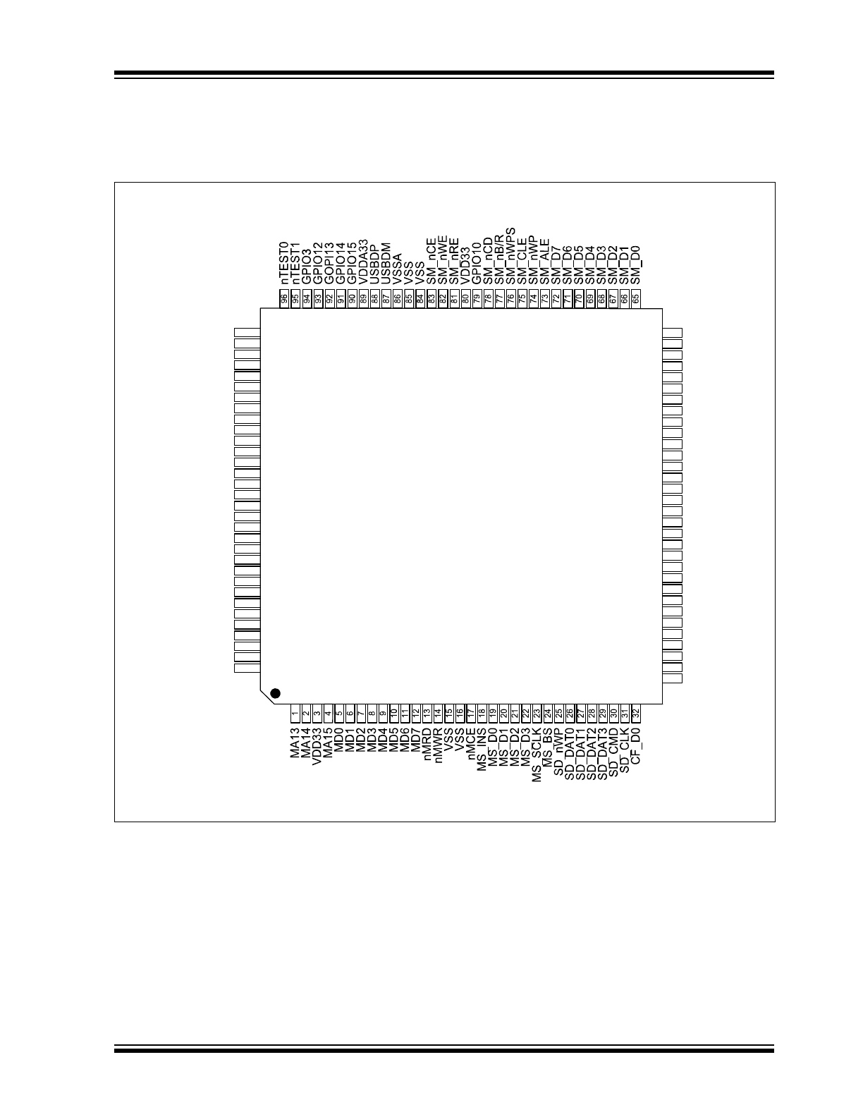
2.0
PIN CONFIGURATION
FIGURE 2-1:
USB2227/USB2228 128-PIN VTQFP
97
VSS
98
RBIAS
99
ATEST
100
VDD33
101
VDD18PLL
102
XTAL1
103
XTAL2
104
VSSPLL
105
GPIO9
106
VDD18
107
GPIO7
108
VDD33
109
GPIO6/ROMEN
110
GPIO5
111
GPIO4
112
VSS
113
GPIO2
114
GPIO1
115
nRESET
116
MA0
117
MA1
118
MA2
119
MA3
120
MA4
121
MA5
122
MA6
123
MA7
124
MA8
125
MA9
126
MA10
127
MA11
128
MA12
64
CF_SA2
63
CF_SA1
62
CF_SA0
61
CF_nCS1
60
CF_nCS0
59
CF_nRESET
58
CF_nIOW
57
CF_nIOR
56
CF_IORDY
55
CF_IRQ
54
CF_nCD2
53
CF_nCD1
52
CF_D15
51
CF_D14
50
CF_D13
49
VDD18
48
CF_D12
47
VSS
46
CF_D11
45
CF_D10
44
GPIO11
43
VDD33
42
GPIO8
41
CF_D9
40
CF_D8
39
CF_D7
38
CF_D6
37
CF_D5
36
CF_D4
35
CF_D3
34
CF_D2
33
CF_D1
USB2227/2228
VTQFP 128
(Top View)
USB2227/USB2228
DS000022
56A-page 6
2007-
2016 Microchip T
e
chnolo
g
y Inc.
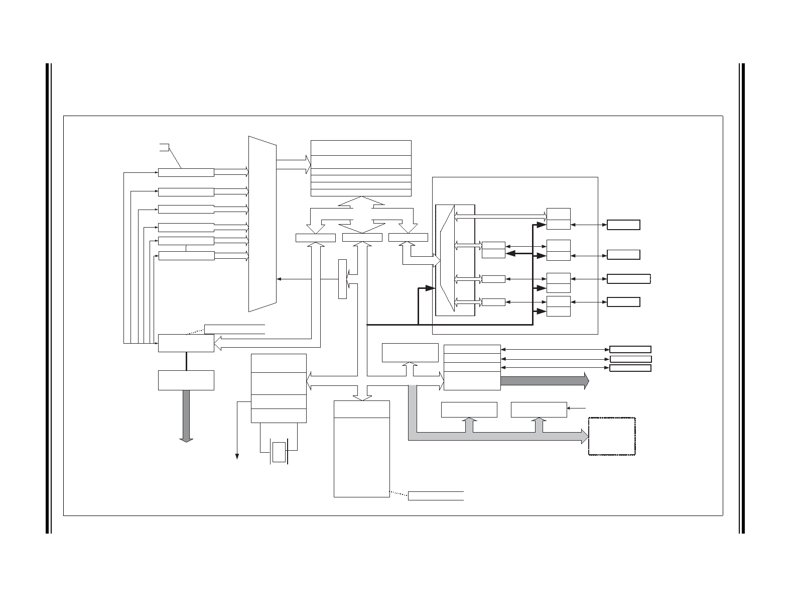
3.0
BLOCK DIAGRAM
FIGURE 3-1:
USB2227/USB2228 BLOCK DIAGRAM
D
a
ta
B
u
s
s
USB 2.0 PHY
( Transciever )
FAST 8051
CPU CORE
GPIO
12 pins
7 pi
ns
Configuration and Control
Clock Generation
X
T
A
L
SIE
( Serial Interface Engine )
Program Memory/ IO
Bus
Interrupt Controller
Latch phase 0, 2
SIE
Latch phase 3
8051
Latch phase 1
FMC
60MHz
32 Bit
Osc
Address
X
D
AT
A &
SF
R
A
ddr
es
s
and D
a
ta
bus
s
e
s
64 Bytes EP0TX
64 Bytes EP0RX
64 Bytes EP1TX
64 Bytes EP1RX
Auto address generators
Ad
d
re
s
s
M
U
X
Data @ 32 bit
15Mhz
SIE Control Regs
Address
Address
Address
Address
EP0RX_BC
RAMRD_A/B
EP0TX_BC
RAMWR_A/B
32 bit 15MHz Data Buss
CLOCKOUT
24 MHz
512 Bytes EP2 TX/RX Buffer A
A
d
d
r
es
s R
e
g
ist
er
1.25KB
SRAM
12K Byte
Scratchpad
SRAM
#LOCKED
#LOCKED
512 Bytes EP2 TX/RX Buffer B
Memory
Cards
Scratchpad
SRAM (768 Byte )
F
M
C Da
ta
M
U
X
ECC
Control/
Status
SD
Controller
SD/MMC
Flash Media
Controllers
(FMC)
Control/
Status
MS
Controller
MS/HS MS/MS PRO
Control/
Status
SM
Controller
SM/SSFDC
Control/
Status
CF
Controller
CF
Control/
Status
CRC
MEM/IO Bus 29pins
DATA
DATA
DATA
DATA
CRC
EP1TX_BC
EP1RX_BC
Address
Address
Flash Media DMA Unit
64K ROM
ROMEN
PWR_FET0
PWR_FET1
PWR_FET2
GPIO11/CRD_PWR2
GPIO10/CRD_PWR1
GPIO8/CRD_PWR0
2007-2016 Microchip Technology Inc.
DS00002256A-page 7
USB2227/USB2228
4.0
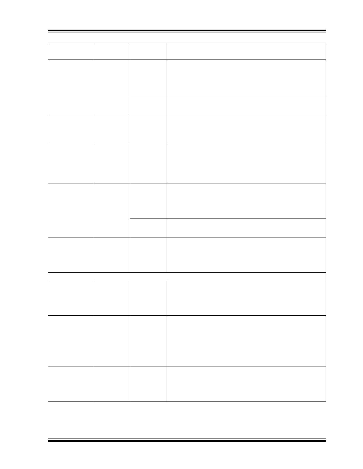
PIN DESCRIPTIONS
This section provides a detailed description of each signal. The signals are arranged in functional groups according to
their associated interface.
The “n” symbol in the signal name indicates that the active, or asserted state occurs when the signal is at a low voltage
level. When “n” is not present before the signal name, the signal is asserted when at the high voltage level.
The terms assertion and negation are used exclusively. This is done to avoid confusion when working with a mixture of
“active low” and “active high” signal. The term assert, or assertion indicates that a signal is active, independent of
whether that level is represented by a high or low voltage. The term negate, or negation indicates that a signal is inactive.
4.1
PIN Descriptions
Symbol
128-Pin
VTQFP
Buffer Type
Description
CompactFlash (In True IDE Mode) Interface
CF_nCS1
61
O8PU
CF Chip Select 1:
This pin is the active low chip select 1 signal for the CF ATA
device.
CF_nCS0
60
O8PU
CF Chip Select 0:
This pin is the active low chip select 0 signal for the task file
registers of CF ATA device in the True IDE mode.
CF_SA2
64
O8
CF Register Address 2:
This pin is the register select address bit 2 for the CF ATA device.
CF_SA1
63
O8
CF Register Address 1:
This pin is the register select address bit 1 for the CF ATA device.
CF_SA0
62
O8
CF Register Address 0:
This pin is the register select address bit 0 for the CF ATA device.
CF_IRQ
55
IPD
CF Interrupt:
This is the active high interrupt request signal from the CF device.
CF_D[15:8]
52
51
50
48
46
45
41
40
I/O8PD
CF Data 15-8:
The bi-directional data signals CF_D15-CF_D8 in True IDE mode
data transfer.
In the True IDE Mode, all of task file register operation occur on
the CF_D[7:0], while the data transfer is on CF_D[15:0].
The bi-directional data signal has an internal weak pull-down
resistor.
CF_D[7:0]
39
38
37
36
35
34
33
32
I/O8PD
CF Data 7-0:
The bi-directional data signals CF_D7-CF_D0 in the True IDE
mode data transfer.
In the True IDE Mode, all of task file register operation occur on
the CF_D[7:0], while the data transfer is on CF_D[15:0].
The bi-directional data signal has an internal weak pull-down
resistor.
CF_IORDY
56
IPU
IO Ready:
This pin is active high input signal.
This pin has an internally controlled weak pull-up resistor.
USB2227/USB2228
DS00002256A-page 8
2007-2016 Microchip Technology Inc.
CF_nCD2
54
IPU
CF Card Detection2:
This card detection pin is connected to the ground on the CF
device, when the CF device is inserted.
This pin has an internally controlled weak pull-up resistor.
CF_nCD1
53
IPU
CF Card Detection1:
This card detection pin is connected to ground on the CF device,
when the CF device is inserted.
This pin has an internally controlled weak pull-up resistor.
CF_nRESET
59
O8
CF Hardware Reset:
This pin is an active low hardware reset signal to CF device.
CF_nIOR
57
O8
CF IO Read:
This pin is an active low read strobe signal for CF device.
CF_nIOW
58
O8
CF IO Write Strobe:
This pin is an active low write strobe signal for CF device.
SmartMedia Interface
SM_nWP
74
O8PD
SM Write Protect:
This pin is an active low write protect signal for the SM device.
This pin has a weak pull-down resistor that is permanently
enabled.
SM_ALE
73
O8PD
SM Address Strobe:
This pin is an active high Address Latch Enable signal for the SM
device.
This pin has a weak pull-down resistor that is permanently
enabled.
SM_CLE
75
O8PD
SM Command Strobe:
This pin is an active high Command Latch Enable signal for the
SM device.
This pin has a weak pull-down resistor that is permanently
enabled.
SM_D[7:0]
72
71
70
69
68
67
66
65
I/O8PD
SM Data 7-0:
These pins are the bi-directional data signal SM_D7-SM_D0.
The bi-directional data signal has an internal weak pull-down
resistor.
SM_nRE
81
08PU
SM Read Enable:
This pin is an active low read strobe signal for SM device.
When using the internal FET, this pin has an internal weak pull-
up resistor that is tied to the output of the internal Power FET.
08
If an external FET is used (Internal FET is disabled), then the
internal pull-up is not available (external pull-ups must be used,
and should be connected to the applicable Card Power Supply).
Symbol
128-Pin
VTQFP
Buffer Type
Description
2007-2016 Microchip Technology Inc.
DS00002256A-page 9
USB2227/USB2228
SM_nWE
82
O8PU
SM Write Enable:
This pin is an active low write strobe signal for SM device.
When using the internal FET, this pin has an internal weak pull-
up resistor that is tied to the output of the internal Power FET.
08
If an external FET is used (Internal FET is disabled), then the
internal pull-up is not available (external pull-ups must be used,
and should be connected to the applicable Card Power Supply).
SM_nWPS
76
IPU
SM Write Protect Switch:
A write-protect seal is detected, when this pin is low.
This pin has an internally controlled weak pull-up resistor.
SM_nB/R
77
I
SM Busy or Data Ready:
This pin is connected to the BSY/RDY pin of the SM device.
An external pull-up resistor is required on this signal. The pull-up
resistor must be pulled up to the same power source that powers
the SM/NAND flash device.
SM_nCE
83
O8PU
SM Chip Enable:
This pin is the active low chip enable signal to the SM device.
When using the internal FET, this pin has an internal weak pull-
up resistor that is tied to the output of the internal Power FET.
08
If an external FET is used (Internal FET is disabled), then the
internal pull-up is not available (external pull-ups must be used,
and should be connected to the applicable Card Power Supply).
SM_nCD
78
IPU
SM Card Detection:
This is the card detection signal from SM device to indicate if the
device is inserted.
This pin has an internally controlled weak pull-up resistor.
Memory Stick Interface
MS_BS
24
O8
MS Bus State:
This pin is connected to the BS pin of the MS device.
It is used to control the Bus States 0, 1, 2 and 3 (BS0, BS1, BS2
and BS3) of the MS device.
MS_SDIO/MS_D
0
19
I/O8PD
MS System Data In/Out:
This pin is a bi-directional data signal for the MS device.
Most significant bit (MSB) of each byte is transmitted first by
either MSC or MS device.
The bi-directional data signal has an internal weak pull-down
resistor.
MS_D1
20
I/O8PD
MS System Data In/Out:
This pin is a bi-directional data signal for the MS device.
This pin has internally controlled weak pull-up and pull-down
resistors for various operational modes.
Symbol
128-Pin
VTQFP
Buffer Type
Description
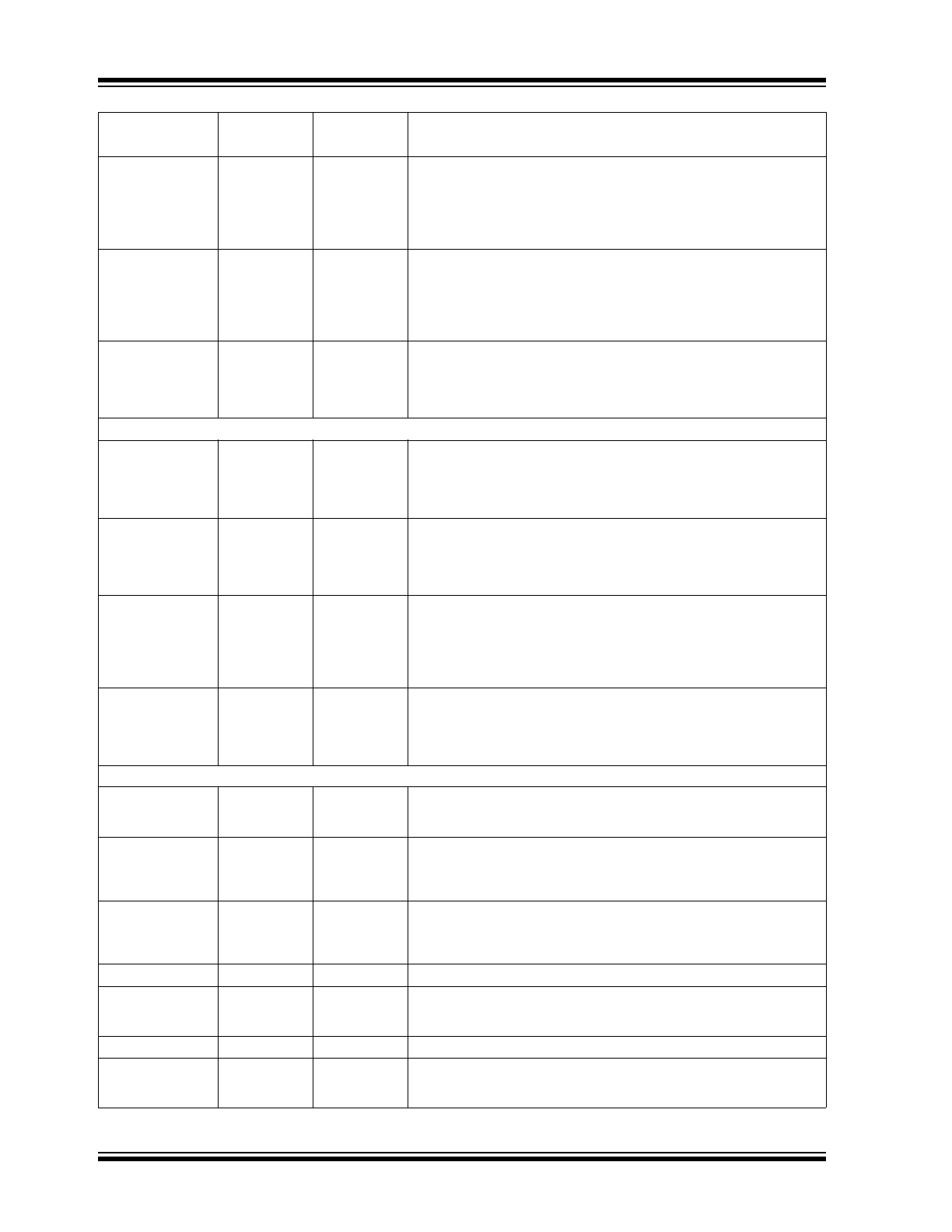
USB2227/USB2228
DS00002256A-page 10
2007-2016 Microchip Technology Inc.
MS_D[3:2]
22
21
I/O8PD
MS System Data In/Out:
This pin is a bi-directional data signal for the MS device.
The bi-directional data signal has an internal weak pull-down
resistor.
MS_INS
18
IPU
MS Card Insertion:
This pin is the card detection signal from the MS device to
indicate, if the device is inserted.
This pin has an internally controlled weak pull-up resistor.
MS_SCLK
23
O8
MS System CLK:
This pin is an output clock signal to the MS device.
The clock frequency is software configurable.
SD Interface
SD_DAT[3:0]
29
28
27
26
I/O8PU
SD Data 3-0:
These are bi-directional data signals.
These pins have internally controlled weak pull-up resistors.
SD_CLK
31
O8
SD Clock:
This is an output clock signal to SD/MMC device.
The clock frequency is software configurable.
SD_CMD
30
I/O8PU
SD Command:
This is a bi-directional signal that connects to the CMD signal of
SD/MMC device.
This pin has an internally controlled weak pull-up resistor.
SD_nWP
25
IPD
SD Write Protected:
This pin is an input signal with an internal weak pull-down.
This pin has an internally controlled weak pull-down resistor.
USB Interface
USBDM
USBDP
87
88
IO-U
USB Bus Data:
These pins connect to the USB bus data signals.
RBIAS
98
I
USB Transceiver Bias:
A 12.0k
, 1.0% resistor is attached from VSSA to this pin, in
order to set the transceiver’s internal bias currents.
ATEST
99
AIO
Analog Test:
This signal is used for testing the analog section of the chip and
should be connected to VDDA33 for normal operation.
VDD18PLL
101
1.8v Power for the PLL
VSSPLL
104
PLL Ground Reference:
Ground Reference for 1.8v PLL power
VDDA33
89
3.3v Analog Power
VSSA
86
Analog Ground Reference:
Analog Ground Reference for 3.3v Analog Power.
Symbol
128-Pin
VTQFP
Buffer Type
Description
2007-2016 Microchip Technology Inc.
DS00002256A-page 1
Highlights
• Complete System Solution for interfacing Smart-
Media
™
(SM) or xD Picture Card
™
(xD)
1
, Memory
Stick
®
(MS), High Speed Memory Stick (HSMS),
Memory Stick PRO (MSPRO), MS Duo
™
, Secure
Digital (SD), Mini-Secure Digital (Mini-SD), Trans-
Flash (SD), MultiMediaCard
™
(MMC), Reduced
Size MultiMediaCard (RS-MMC), NAND Flash,
Compact Flash
®
(CF) and CF Ultra
™
I & II, and
CF form-factor ATA hard drives to USB 2.0 bus
- Supports USB Bulk Only Mass Storage Com-
pliant Bootable BIOS
• Support for simultaneous operation of all above
devices. (only one at a time of each of the follow-
ing groups supported: CF or ATA drive, SM or XD
or NAND, SD or MMC)
• On-Chip 4-Bit High Speed Memory Stick and MS
PRO Hardware Circuitry
• On-Chip firmware reads and writes High Speed
Memory Stick and MS PRO
• 1-bit ECC correction performed in hardware for
maximum efficiency
• Hardware support for SD Security Command
Extensions
• On-chip power FETs for supplying flash media
card power with minimum board components
• USB Bus Power Certified
• 3.3 Volt I/O with 5V input tolerance on VBUS/
GPIO3
• Complete USB Specification 2.0 Compatibility for
Bus Powered Operation
- Includes USB 2.0 Transceiver
- A Bi-directional Control and a Bi-directional
Bulk Endpoint are provided.
• 8051 8 bit microprocessor
- Provides low speed control functions
- 30 Mhz execution speed at 4 cycles per
instruction average
- 12K Bytes of internal SRAM for general pur-
pose scratchpad
- 768 Bytes of internal SRAM for general pur-
pose scratchpad or program execution while
re-flashing external ROM
• Double Buffered Bulk Endpoint
- Bi-directional 512 Byte Buffer for Bulk End-
point
- 64 Byte RX Control Endpoint Buffer
- 64 Byte TX Control Endpoint Buffer
• Internal or External Program Memory Interface
- 64K Byte Internal Code Space or Optional
64K Byte External Code Space using Flash,
SRAM or EPROM memory.
• On Board 24Mhz Crystal Driver Circuit
• Can be clocked by 48MHz external source
• On-Chip 1.8V Regulator for Low Power Core
Operation
• Internal PLL for 480Mhz USB 2.0 Sampling, Con-
figurable MCU clock
• Supports firmware upgrade via USB bus if “boot
block” Flash program memory is used
• 15 GPIOs for special function use: LED indica-
tors, button inputs, power control to memory
devices, etc.
- Inputs capable of generating interrupts with
either edge sensitivity
- Attribute bit controlled features:
- Activity LED polarity/operation/blink rate
- Full or Partial Card compliance checking
- Bus or Self Powered
- LUN configuration and assignment
- Write Protect Polarity
- SmartDetach Detach from USB when no
Card Inserted for Notebook apps
- Cover Switch operation for xD compliance
- Inquiry Command operation
- SD Write Protect operation
- Older CF card support
- Force USB 1.1 reporting
- Internal or External Power FET operation
• Compatible with Microsoft WinXP, WinME, Win2K
SP3, Apple OS10, Softconnex, and Linux Multi-
LUN Mass Storage Class Drivers
• Win2K, Win98/98SE and Apple OS8.6 and OS9
Multi-LUN Mass Storage Class Drivers available
from Microchip
• 128-Pin VTQFP RoHS Compliant Package
(14mm x 14mm footprint, 1.0mm height)
1.xD Picture Card not applicable to USB2227
USB2227/USB2228
4th Generation USB 2.0 Flash Media Controller with
Integrated Card Power FETs
USB2227/USB2228
DS00002256A-page 2
2007-2016 Microchip Technology Inc.
TO OUR VALUED CUSTOMERS
It is our intention to provide our valued customers with the best documentation possible to ensure successful use of your Microchip
products. To this end, we will continue to improve our publications to better suit your needs. Our publications will be refined and
enhanced as new volumes and updates are introduced.
If you have any questions or comments regarding this publication, please contact the Marketing Communications Department via
E-mail at
docerrors@microchip.com
. We welcome your feedback.
Most Current Data Sheet
To obtain the most up-to-date version of this data sheet, please register at our Worldwide Web site at:
http://www.microchip.com
You can determine the version of a data sheet by examining its literature number found on the bottom outside corner of any page.
The last character of the literature number is the version number, (e.g., DS30000000A is version A of document DS30000000).
Errata
An errata sheet, describing minor operational differences from the data sheet and recommended workarounds, may exist for cur-
rent devices. As device/documentation issues become known to us, we will publish an errata sheet. The errata will specify the
revision of silicon and revision of document to which it applies.
To determine if an errata sheet exists for a particular device, please check with one of the following:
• Microchip’s Worldwide Web site;
http://www.microchip.com
• Your local Microchip sales office (see last page)
When contacting a sales office, please specify which device, revision of silicon and data sheet (include -literature number) you are
using.
Customer Notification System
Register on our web site at
www.microchip.com
to receive the most current information on all of our products.
2007-2016 Microchip Technology Inc.
DS00002256A-page 3
USB2227/USB2228
Table of Contents
1.0 General Description ........................................................................................................................................................................ 4
2.0 Pin Configuration ............................................................................................................................................................................ 5
3.0 Block Diagram ................................................................................................................................................................................. 6
4.0 Pin Descriptions .............................................................................................................................................................................. 7
5.0 DC Parameters ............................................................................................................................................................................. 15
6.0 Package Information ..................................................................................................................................................................... 19
7.0 GPIO Usage .................................................................................................................................................................................. 20
Appendix A: Data Sheet Revision History ........................................................................................................................................... 21
The Microchip Web Site ...................................................................................................................................................................... 22
Customer Change Notification Service ............................................................................................................................................... 22
Customer Support ............................................................................................................................................................................... 22
Product Identification System ............................................................................................................................................................. 23
USB2227/USB2228
DS00002256A-page 4
2007-2016 Microchip Technology Inc.
1.0
GENERAL DESCRIPTION
The USB2227/USB2228 is a USB 2.0 Bulk Only Mass Storage Class Peripheral Controller intended for supporting Com-
pactFlash (CF and CF Ultra I/II) in True IDE Mode only, SmartMedia (SM) and XD cards, Memory Stick (MS), Memory
Stick DUO (MSDUO) and Memory Stick Pro (MSPRO), Secure Digital (SD), and MultiMediaCard (MMC) flash memory
devices. It provides a single chip solution for the most popular flash memory cards in the market.
The device consists of a USB 2.0 PHY and SIE, buffers, Fast 8051 microprocessor with expanded scratchpad, and pro-
gram SRAM, and CF, MS, SM and SD controllers. The SD controller supports both SD and MMC devices. SM controller
supports both SM and xD cards.
Provisions for external Flash Memory up to 64K bytes for program storage is provided.
12K bytes of scratchpad SRAM and 768 Bytes of program SRAM are also provided.
Fifteen GPIO pins are provided for indicators, external serial EEPROM for OEM id and system configuration information,
and other special functions.
Internal power FETs are provided to directly supply power to the xD/SM, MMC/SD and MS/MSPro cards.
The internal ROM program is capable of implementing any combination of single or multi-LUN CF/SD/MMC/SM/MS
reader functions with individual card power control and activity indication. Microchip also provides licenses** for Win98
and Win2K drivers and setup utilities. Note: Please check with Microchip for precise features and capabilities for the
current ROM code release.
1.1
Acronyms
SM:
SmartMedia
SMC:
SmartMedia Controller
FM:
Flash Media
FMC:
Flash Media Controller
CF:
Compact Flash
CFC:
CompactFlash Controller
SD:
Secure Digital
SDC:
Secure Digital Controller
MMC:
MultiMediaCard
MS:
Memory Stick
MSC:
Memory Stick Controller
TPC:
Transport Protocol Code.
ECC:
Error Checking and Correcting
CRC:
Cyclic Redundancy Checking
2007-2016 Microchip Technology Inc.
DS00002256A-page 5
USB2227/USB2228
2.0
PIN CONFIGURATION
FIGURE 2-1:
USB2227/USB2228 128-PIN VTQFP
97
VSS
98
RBIAS
99
ATEST
100
VDD33
101
VDD18PLL
102
XTAL1
103
XTAL2
104
VSSPLL
105
GPIO9
106
VDD18
107
GPIO7
108
VDD33
109
GPIO6/ROMEN
110
GPIO5
111
GPIO4
112
VSS
113
GPIO2
114
GPIO1
115
nRESET
116
MA0
117
MA1
118
MA2
119
MA3
120
MA4
121
MA5
122
MA6
123
MA7
124
MA8
125
MA9
126
MA10
127
MA11
128
MA12
64
CF_SA2
63
CF_SA1
62
CF_SA0
61
CF_nCS1
60
CF_nCS0
59
CF_nRESET
58
CF_nIOW
57
CF_nIOR
56
CF_IORDY
55
CF_IRQ
54
CF_nCD2
53
CF_nCD1
52
CF_D15
51
CF_D14
50
CF_D13
49
VDD18
48
CF_D12
47
VSS
46
CF_D11
45
CF_D10
44
GPIO11
43
VDD33
42
GPIO8
41
CF_D9
40
CF_D8
39
CF_D7
38
CF_D6
37
CF_D5
36
CF_D4
35
CF_D3
34
CF_D2
33
CF_D1
USB2227/2228
VTQFP 128
(Top View)
USB2227/USB2228
DS000022
56A-page 6
2007-
2016 Microchip T
e
chnolo
g
y Inc.
3.0
BLOCK DIAGRAM
FIGURE 3-1:
USB2227/USB2228 BLOCK DIAGRAM
D
a
ta
B
u
s
s
USB 2.0 PHY
( Transciever )
FAST 8051
CPU CORE
GPIO
12 pins
7 pi
ns
Configuration and Control
Clock Generation
X
T
A
L
SIE
( Serial Interface Engine )
Program Memory/ IO
Bus
Interrupt Controller
Latch phase 0, 2
SIE
Latch phase 3
8051
Latch phase 1
FMC
60MHz
32 Bit
Osc
Address
X
D
AT
A &
SF
R
A
ddr
es
s
and D
a
ta
bus
s
e
s
64 Bytes EP0TX
64 Bytes EP0RX
64 Bytes EP1TX
64 Bytes EP1RX
Auto address generators
Ad
d
re
s
s
M
U
X
Data @ 32 bit
15Mhz
SIE Control Regs
Address
Address
Address
Address
EP0RX_BC
RAMRD_A/B
EP0TX_BC
RAMWR_A/B
32 bit 15MHz Data Buss
CLOCKOUT
24 MHz
512 Bytes EP2 TX/RX Buffer A
A
d
d
r
es
s R
e
g
ist
er
1.25KB
SRAM
12K Byte
Scratchpad
SRAM
#LOCKED
#LOCKED
512 Bytes EP2 TX/RX Buffer B
Memory
Cards
Scratchpad
SRAM (768 Byte )
F
M
C Da
ta
M
U
X
ECC
Control/
Status
SD
Controller
SD/MMC
Flash Media
Controllers
(FMC)
Control/
Status
MS
Controller
MS/HS MS/MS PRO
Control/
Status
SM
Controller
SM/SSFDC
Control/
Status
CF
Controller
CF
Control/
Status
CRC
MEM/IO Bus 29pins
DATA
DATA
DATA
DATA
CRC
EP1TX_BC
EP1RX_BC
Address
Address
Flash Media DMA Unit
64K ROM
ROMEN
PWR_FET0
PWR_FET1
PWR_FET2
GPIO11/CRD_PWR2
GPIO10/CRD_PWR1
GPIO8/CRD_PWR0
2007-2016 Microchip Technology Inc.
DS00002256A-page 7
USB2227/USB2228
4.0
PIN DESCRIPTIONS
This section provides a detailed description of each signal. The signals are arranged in functional groups according to
their associated interface.
The “n” symbol in the signal name indicates that the active, or asserted state occurs when the signal is at a low voltage
level. When “n” is not present before the signal name, the signal is asserted when at the high voltage level.
The terms assertion and negation are used exclusively. This is done to avoid confusion when working with a mixture of
“active low” and “active high” signal. The term assert, or assertion indicates that a signal is active, independent of
whether that level is represented by a high or low voltage. The term negate, or negation indicates that a signal is inactive.
4.1
PIN Descriptions
Symbol
128-Pin
VTQFP
Buffer Type
Description
CompactFlash (In True IDE Mode) Interface
CF_nCS1
61
O8PU
CF Chip Select 1:
This pin is the active low chip select 1 signal for the CF ATA
device.
CF_nCS0
60
O8PU
CF Chip Select 0:
This pin is the active low chip select 0 signal for the task file
registers of CF ATA device in the True IDE mode.
CF_SA2
64
O8
CF Register Address 2:
This pin is the register select address bit 2 for the CF ATA device.
CF_SA1
63
O8
CF Register Address 1:
This pin is the register select address bit 1 for the CF ATA device.
CF_SA0
62
O8
CF Register Address 0:
This pin is the register select address bit 0 for the CF ATA device.
CF_IRQ
55
IPD
CF Interrupt:
This is the active high interrupt request signal from the CF device.
CF_D[15:8]
52
51
50
48
46
45
41
40
I/O8PD
CF Data 15-8:
The bi-directional data signals CF_D15-CF_D8 in True IDE mode
data transfer.
In the True IDE Mode, all of task file register operation occur on
the CF_D[7:0], while the data transfer is on CF_D[15:0].
The bi-directional data signal has an internal weak pull-down
resistor.
CF_D[7:0]
39
38
37
36
35
34
33
32
I/O8PD
CF Data 7-0:
The bi-directional data signals CF_D7-CF_D0 in the True IDE
mode data transfer.
In the True IDE Mode, all of task file register operation occur on
the CF_D[7:0], while the data transfer is on CF_D[15:0].
The bi-directional data signal has an internal weak pull-down
resistor.
CF_IORDY
56
IPU
IO Ready:
This pin is active high input signal.
This pin has an internally controlled weak pull-up resistor.
USB2227/USB2228
DS00002256A-page 8
2007-2016 Microchip Technology Inc.
CF_nCD2
54
IPU
CF Card Detection2:
This card detection pin is connected to the ground on the CF
device, when the CF device is inserted.
This pin has an internally controlled weak pull-up resistor.
CF_nCD1
53
IPU
CF Card Detection1:
This card detection pin is connected to ground on the CF device,
when the CF device is inserted.
This pin has an internally controlled weak pull-up resistor.
CF_nRESET
59
O8
CF Hardware Reset:
This pin is an active low hardware reset signal to CF device.
CF_nIOR
57
O8
CF IO Read:
This pin is an active low read strobe signal for CF device.
CF_nIOW
58
O8
CF IO Write Strobe:
This pin is an active low write strobe signal for CF device.
SmartMedia Interface
SM_nWP
74
O8PD
SM Write Protect:
This pin is an active low write protect signal for the SM device.
This pin has a weak pull-down resistor that is permanently
enabled.
SM_ALE
73
O8PD
SM Address Strobe:
This pin is an active high Address Latch Enable signal for the SM
device.
This pin has a weak pull-down resistor that is permanently
enabled.
SM_CLE
75
O8PD
SM Command Strobe:
This pin is an active high Command Latch Enable signal for the
SM device.
This pin has a weak pull-down resistor that is permanently
enabled.
SM_D[7:0]
72
71
70
69
68
67
66
65
I/O8PD
SM Data 7-0:
These pins are the bi-directional data signal SM_D7-SM_D0.
The bi-directional data signal has an internal weak pull-down
resistor.
SM_nRE
81
08PU
SM Read Enable:
This pin is an active low read strobe signal for SM device.
When using the internal FET, this pin has an internal weak pull-
up resistor that is tied to the output of the internal Power FET.
08
If an external FET is used (Internal FET is disabled), then the
internal pull-up is not available (external pull-ups must be used,
and should be connected to the applicable Card Power Supply).
Symbol
128-Pin
VTQFP
Buffer Type
Description
2007-2016 Microchip Technology Inc.
DS00002256A-page 9
USB2227/USB2228
SM_nWE
82
O8PU
SM Write Enable:
This pin is an active low write strobe signal for SM device.
When using the internal FET, this pin has an internal weak pull-
up resistor that is tied to the output of the internal Power FET.
08
If an external FET is used (Internal FET is disabled), then the
internal pull-up is not available (external pull-ups must be used,
and should be connected to the applicable Card Power Supply).
SM_nWPS
76
IPU
SM Write Protect Switch:
A write-protect seal is detected, when this pin is low.
This pin has an internally controlled weak pull-up resistor.
SM_nB/R
77
I
SM Busy or Data Ready:
This pin is connected to the BSY/RDY pin of the SM device.
An external pull-up resistor is required on this signal. The pull-up
resistor must be pulled up to the same power source that powers
the SM/NAND flash device.
SM_nCE
83
O8PU
SM Chip Enable:
This pin is the active low chip enable signal to the SM device.
When using the internal FET, this pin has an internal weak pull-
up resistor that is tied to the output of the internal Power FET.
08
If an external FET is used (Internal FET is disabled), then the
internal pull-up is not available (external pull-ups must be used,
and should be connected to the applicable Card Power Supply).
SM_nCD
78
IPU
SM Card Detection:
This is the card detection signal from SM device to indicate if the
device is inserted.
This pin has an internally controlled weak pull-up resistor.
Memory Stick Interface
MS_BS
24
O8
MS Bus State:
This pin is connected to the BS pin of the MS device.
It is used to control the Bus States 0, 1, 2 and 3 (BS0, BS1, BS2
and BS3) of the MS device.
MS_SDIO/MS_D
0
19
I/O8PD
MS System Data In/Out:
This pin is a bi-directional data signal for the MS device.
Most significant bit (MSB) of each byte is transmitted first by
either MSC or MS device.
The bi-directional data signal has an internal weak pull-down
resistor.
MS_D1
20
I/O8PD
MS System Data In/Out:
This pin is a bi-directional data signal for the MS device.
This pin has internally controlled weak pull-up and pull-down
resistors for various operational modes.
Symbol
128-Pin
VTQFP
Buffer Type
Description
USB2227/USB2228
DS00002256A-page 10
2007-2016 Microchip Technology Inc.
MS_D[3:2]
22
21
I/O8PD
MS System Data In/Out:
This pin is a bi-directional data signal for the MS device.
The bi-directional data signal has an internal weak pull-down
resistor.
MS_INS
18
IPU
MS Card Insertion:
This pin is the card detection signal from the MS device to
indicate, if the device is inserted.
This pin has an internally controlled weak pull-up resistor.
MS_SCLK
23
O8
MS System CLK:
This pin is an output clock signal to the MS device.
The clock frequency is software configurable.
SD Interface
SD_DAT[3:0]
29
28
27
26
I/O8PU
SD Data 3-0:
These are bi-directional data signals.
These pins have internally controlled weak pull-up resistors.
SD_CLK
31
O8
SD Clock:
This is an output clock signal to SD/MMC device.
The clock frequency is software configurable.
SD_CMD
30
I/O8PU
SD Command:
This is a bi-directional signal that connects to the CMD signal of
SD/MMC device.
This pin has an internally controlled weak pull-up resistor.
SD_nWP
25
IPD
SD Write Protected:
This pin is an input signal with an internal weak pull-down.
This pin has an internally controlled weak pull-down resistor.
USB Interface
USBDM
USBDP
87
88
IO-U
USB Bus Data:
These pins connect to the USB bus data signals.
RBIAS
98
I
USB Transceiver Bias:
A 12.0k
, 1.0% resistor is attached from VSSA to this pin, in
order to set the transceiver’s internal bias currents.
ATEST
99
AIO
Analog Test:
This signal is used for testing the analog section of the chip and
should be connected to VDDA33 for normal operation.
VDD18PLL
101
1.8v Power for the PLL
VSSPLL
104
PLL Ground Reference:
Ground Reference for 1.8v PLL power
VDDA33
89
3.3v Analog Power
VSSA
86
Analog Ground Reference:
Analog Ground Reference for 3.3v Analog Power.
Symbol
128-Pin
VTQFP
Buffer Type
Description