
2004-2013 Microchip Technology Inc.
DS21915C-page 1
MCP73853/55
Features
• Linear Charge Management Controllers
- Integrated Pass Transistor
- Integrated Current Sense
- Reverse Blocking Protection
• High-Accuracy Preset Voltage Regulation: + 0.5%
• Two Selectable Voltage Regulation Options:
- 4.1V, 4.2V
• Programmable Charge Current
• USB Compatible Charge Current Settings
• Programmable Safety Charge Timers
• Preconditioning of Deeply Depleted Cells
• Automatic End-of-Charge Control
• Optional Continuous Cell Temperature Monitoring
MCP73853
• Charge Status Output for Direct LED Drive
• Fault Output for Direct LED Drive
MCP73853
• Automatic Power-Down
• Thermal Regulation
• Temperature Range: -40°C to +85°C
• Packaging:
- 16-Lead, 4x4 mm QFN (MCP73853)
- 10-Lead, 3x3 mm DFN (MCP73855)
Applications
• Lithium-Ion/Lithium-Polymer Battery Chargers
• Personal Data Assistants (PDAs)
• Cellular Telephones
• Hand-Held Instruments
• Cradle Chargers
• Digital Cameras
• MP3 Players
• Bluetooth Headsets
• USB Chargers
Description
The MCP7385X devices are highly-advanced, linear
charge management controllers, for use in space-
limited, cost-sensitive applications. The MCP73853
combines high-accuracy constant-voltage, constant-
current regulation, cell preconditioning, cell temperature
monitoring, advanced safety timers, automatic charge
termination, internal current sensing, reverse blocking
protection and charge status and fault indication in a
space-saving 16-lead, 4x4 QFN package.
The MCP73855 employs all the features of the
MCP73853, with the exception of the cell temperature
monitor and one status output. The MCP73855 is
offered in a space-saving 10-lead, 3x3 DFN package.
The MCP73853 and MCP73855 are designed
specifically for USB applications, adhering to all the
specifications governing the USB power bus.
The MCP7385X devices provide two selectable
voltage regulation options (4.1V or 4.2V) for use with
either coke or graphite anodes.
These devices have complete and fully-functional,
charge management solutions, operating with an input
voltage range of 4.5V to 5.5V. These are fully specified
over the ambient temperature range of -40°C to +85°C.
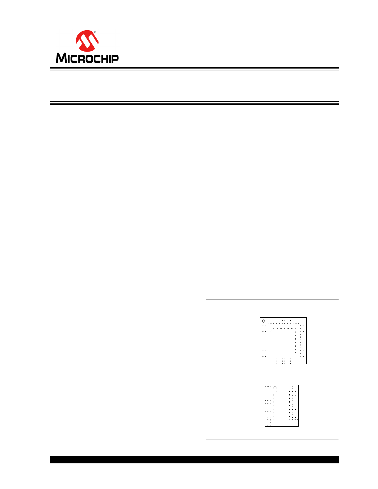
Package Types
2
MCP73853
4x4 QFN*
V
DD2
V
SS1
V
SET
V
BAT3
V
BAT2
PR
O
G
V
BAT1
T
HRE
F
THER
M
TI
MER
V
SS3
ST
A
T
1
ST
A
T
2
EN
V
SS2
V
DD1
EP
16
1
15 14 13
3
4
12
11
10
9
5
6
7
8
17
MCP73855
3x3 DFN*
V
DD1
V
SET
V
SS1
V
BAT2
V
BAT1
1
2
3
4
10
9
8
7
V
SS2
EN
STAT1
EP
11
5
6
PROG
TIMER
*Exposed Pad (EP) is at V
SS
potential.
USB Compatible Li-Ion/Li-Polymer
Charge Management Controllers
MCP73853/55
DS21915C-page 2
2004-2013 Microchip Technology Inc.
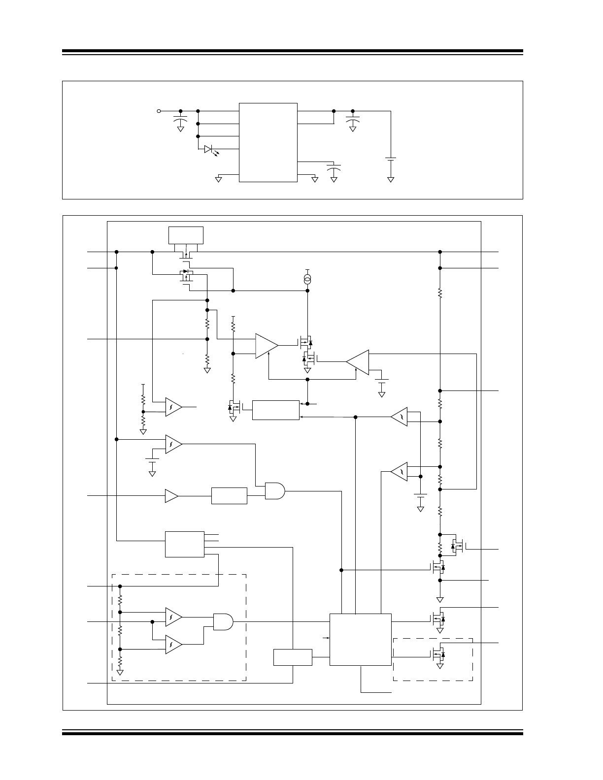
Typical Application
Functional Block Diagram
EN
STAT1
V
SET
V
DD1
V
SS
TIMER
PROG
V
BAT1
V
BAT2
+
–
Single
Lithium-Ion
Cell
3
2
MCP73855
5
6
4, 7
9
8
10
1
5V
4.7 µF
400 mA Lithium-Ion Battery Charger
4.7 µF
0.1 µF
+
–
Charge
Termination
Comparator
Voltage Control
Amplifier
+
–
U
VLO
COMPARATOR
V
UVLO
+
-
Temperature
Comparators
+
-
Bias and
Reference
Generator
V
UVLO
V
REF
(1.2V)
Power-On
Delay
+
–
+
–
V
REF
V
REF
Oscillator
I
REG
/12
Constant-voltage/
Recharge Comp.
Precondition
Control
Charge_OK
Precon.
V
DD
Charge Current
Control Amplifier
+
–
V
REF
V
REF
+
–
Precondition
Comp
.
Charge Control,
Charge Timers,
and
Status Logic
Drv Stat 2
Drv Stat 1
Charge_OK
I
REG
/12
V
DD1
THERM
EN
TIMER
STAT1
STAT2
V
BAT3
V
SS1
PROG
V
SET
THREF
V
BAT1
90
110 k
10 k
10 k
100 k
50 k
50 k
G = 0.001
11 k
3 k
600 k
149 k
1.58 k
V
DD2
V
BAT2
300 k
10.3 k
4 k
Direction
Control
k
V
SS2
V
SS3
MCP73853 ONLY
MCP73853 ONLY
2004-2013 Microchip Technology Inc.
DS21915C-page 3
MCP73853/55
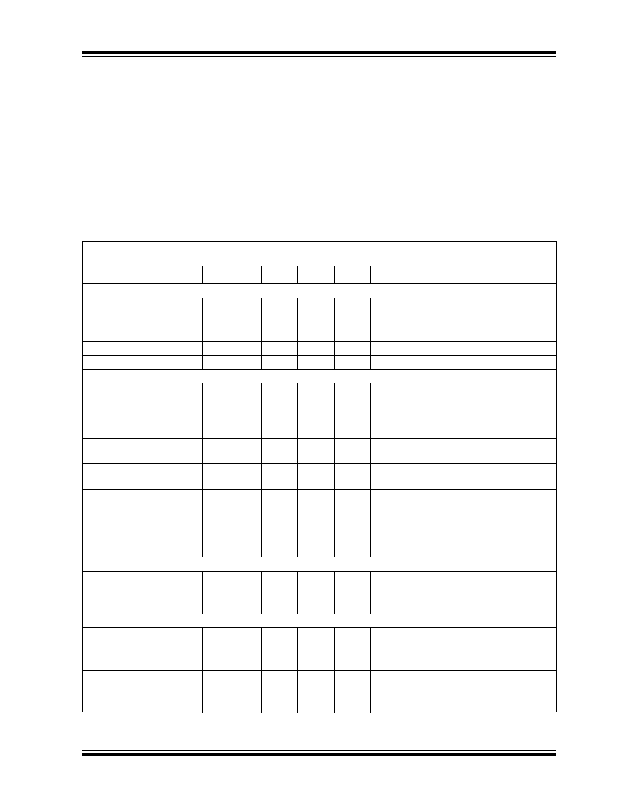
1.0
ELECTRICAL
CHARACTERISTICS
Absolute Maximum Ratings*
V
DD1,2
.............................................................................6.5V
All Inputs and Outputs w.r.t. V
SS
..............-0.3 to (V
DD
+ 0.3)V
Maximum Junction Temperature, T
J
............ Internally Limited
Storage temperature .....................................-65°C to +150°C
ESD protection on all pins:
Human Body Model (1.5k
in Series with 100pF) 4 kV
Machine Model (200pF, No Series Resistance) ..........400V
*Notice: Stresses above those listed under “Maximum
Ratings” may cause permanent damage to the device. This is
a stress rating only and functional operation of the device at
those or any other conditions above those indicated in the
operational listings of this specification is not implied.
Exposure to maximum rating conditions for extended periods
may affect device reliability.
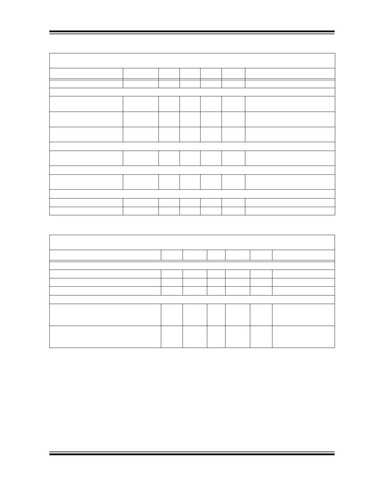
DC CHARACTERISTICS
Electrical Specifications: Unless otherwise indicated, all limits apply for V
DD
= [V
REG
(Typ) + 0.3V] to 5.5V,
T
A
= -40°C to 85°C. Typical values are at +25°C, V
DD
= [V
REG
(Typ) + 1.0V]
Parameters
Sym
Min
Typ
Max
Units
Conditions
Supply Input
Supply Voltage
V
DD
4.5
—
5.5
V
Supply Current
I
SS
—
0.28
4
µA
Disabled
—
0.83
4
mA Operating
UVLO Start Threshold
V
START
4.25
4.45
4.65
V
V
DD
Low-to-High
UVLO Stop Threshold
V
STOP
4.20
4.40
4.55
V
V
DD
High-to-Low
Voltage Regulation (Constant-Voltage Mode)
Regulated Output Voltage
V
REG
4.079
4.1
4.121
V
V
SET
= V
SS
4.179
4.2
4.221
V
V
SET
= V
DD
V
DD
= [V
REG
(Typ) + 1V],
I
OUT
= 10 mA, T
A
= -5°C to +55°C
Line Regulation
V
BAT
/
V
BAT
)| /
V
DD
—
0.020
0.25
%/V V
DD
= [V
REG
(Typ) + 1V] to 5.5V
I
OUT
= 10 mA
Load Regulation
V
BAT
/V
BAT
|
—
0.022
0.25
%
I
OUT
= 10 mA to 150 mA
V
DD
= [V
REG
(Typ) + 1V]
Supply Ripple Attenuation
PSRR
—
50
—
dB
I
OUT
= 10 mA, 10 Hz to 1 kHz
—
26
—
dB
I
OUT
= 10 mA, 10 Hz to 10 kHz
—
24
—
dB
I
OUT
= 10 mA, 10 Hz to 1 MHz
Output Reverse-Leakage
Current
I
DISCHARGE
—
0.24
1
µA
V
DD
< V
BAT
= V
REG
(Typ)
Current Regulation (Fast Charge Constant-Current Mode)
Fast Charge Current
Regulation
I
REG
70
85
100
mA PROG = OPEN
325
400
475
mA PROG = V
SS
T
A
= -5°C to +55°C
Preconditioning Current Regulation (Trickle Charge Constant-Current Mode)
Precondition Current
Regulation
I
PREG
5
9
15
mA PROG = OPEN
25
40
75
mA PROG = V
SS
T
A
= -5°C to +55°C
Precondition Threshold
Voltage
V
PTH
2.70
2.80
2.90
V
V
SET
= V
SS
2.75
2.85
2.95
V
V
SET
= V
DD
V
BAT
Low-to-High
MCP73853/55
DS21915C-page 4
2004-2013 Microchip Technology Inc.
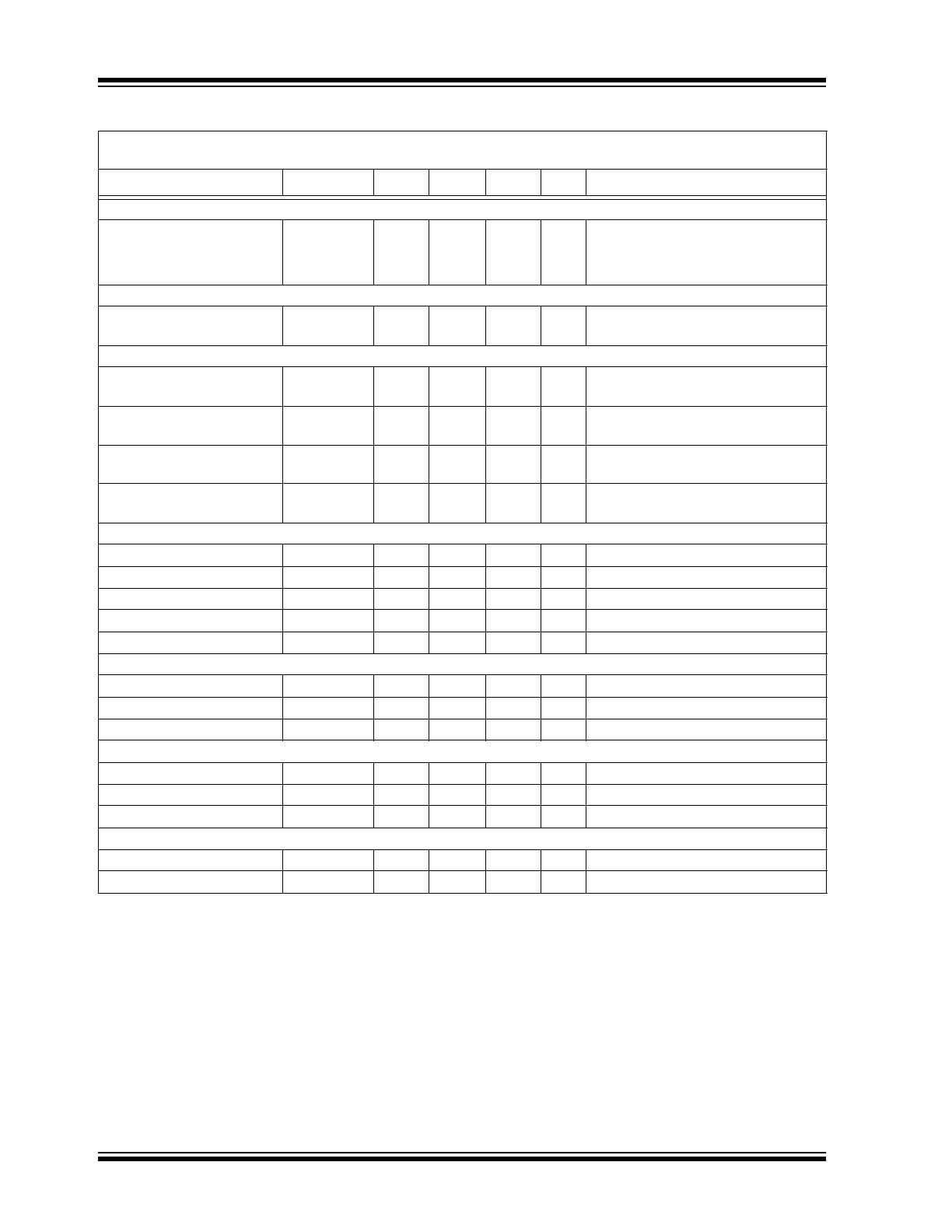
Charge Termination
Charge Termination Current
I
TERM
3.7
6.5
9.3
mA PROG = OPEN
18
32
46
mA PROG = V
SS
T
A
= -5°C to +55°C
Automatic Recharge
Recharge Threshold Voltage
V
RTH
V
REG
–
300mV
V
REG
–
200mV
V
REG
–
100mV
V
V
BAT
High-to-Low
Thermistor Reference - MCP73853
Thermistor Reference
Output Voltage
V
THREF
2.475
2.55
2.625
V
T
A
= 25°C, V
DD
= V
REG
(Typ) + 1V,
I
THREF
= 0 mA
Thermistor Reference
Source Current
I
THREF
200
—
—
µA
Thermistor Reference Line
Regulation
V
THREF
/
V
THREF
)|/
V
DD
—
0.05
0.25
%/V V
DD
= [V
REG
(Typ) + 1V] to 5.5V
Thermistor Reference Load
Regulation
V
THREF
/
V
THREF|
0.02
0.10
%
I
THREF
= 0 mA to 0.20 mA
Thermistor Comparator - MCP73853
Upper Trip Threshold
V
T1
1.18
1.25
1.32
V
Upper Trip Point Hysteresis
V
T1HYS
—
-50
—
mV
Lower Trip Threshold
V
T2
0.59
0.62
0.66
V
Lower Trip Point Hysteresis
V
T2HYS
—
80
—
mV
Input Bias Current
I
BIAS
—
—
2
A
Status Indicator – STAT1, STAT2
Sink Current
I
SINK
4
8
12
mA
Low Output Voltage
V
OL
—
200
400
mV I
SINK
= 1 mA
Input Leakage Current
I
LK
—
0.01
1
A I
SINK
= 0 mA, V
STAT1,2
= 5.5V
Enable Input
Input High Voltage Level
V
IH
1.4
—
—
V
Input Low Voltage Level
V
IL
—
—
0.8
V
Input Leakage Current
I
LK
—
0.01
1
A V
ENABLE
= 5.5V
Thermal Shutdown
Die Temperature
T
SD
—
155
—
°C
Die Temperature Hysteresis
T
SDHYS
—
10
—
°C
DC CHARACTERISTICS (Continued)
Electrical Specifications: Unless otherwise indicated, all limits apply for V
DD
= [V
REG
(Typ) + 0.3V] to 5.5V,
T
A
= -40°C to 85°C. Typical values are at +25°C, V
DD
= [V
REG
(Typ) + 1.0V]
Parameters
Sym
Min
Typ
Max
Units
Conditions
2004-2013 Microchip Technology Inc.
DS21915C-page 5
MCP73853/55
TEMPERATURE SPECIFICATIONS
AC CHARACTERISTICS
Electrical Specifications: Unless otherwise indicated, all limits apply for V
DD
= [V
REG
(Typ) + 0.3V] to 5.5V,
T
A
= -40°C to 85°C. Typical values are at +25°C, V
DD
= [V
REG
(Typ) + 1.0V]
Parameters
Sym
Min
Typ
Max
Units
Conditions
UVLO Start Delay
t
START
—
—
5
ms
V
DD
Low-to-High
Current Regulation
Transition Time Out of
Preconditioning
t
DELAY
—
—
1
ms
V
BAT
< V
PTH
to V
BAT
> V
PTH
Current Rise Time Out of
Preconditioning
t
RISE
—
—
1
ms
I
OUT
Rising to 90% of I
REG
Fast Charge Safety Timer
Period
t
FAST
1.1
1.5
1.9
Hours
C
TIMER
= 0.1 µF
Preconditioning Current Regulation
Preconditioning Charge
Safety Timer Period
t
PRECON
45
60
75
Minutes C
TIMER
= 0.1 µF
Charge Termination
Elapsed Time Termination
Period
t
TERM
2.2
3
3.8
Hours
C
TIMER
= 0.1 µF
Status Indicators
Status Output Turn-off
t
OFF
—
—
200
µs
I
SINK
= 1 mA to 0 mA
Status Output Turn-on
t
ON
—
—
200
µs
I
SINK
= 0 mA to 1 mA
Electrical Specifications: Unless otherwise indicated, all limits apply for V
DD
= [V
REG
(Typ) + 0.3V] to 5.5.
Typical values are at +25°C, V
DD
= [V
REG
(Typ) + 1.0V]
Parameters
Sym
Min
Typ
Max
Units
Conditions
Temperature Ranges
Specified Temperature Range
T
A
-40
—
+85
°C
Operating Temperature Range
T
J
-40
—
+125
°C
Storage Temperature Range
T
A
-65
—
+150
°C
Thermal Package Resistances
Thermal Resistance, 16-L, 4mm x 4mm QFN
JA
—
37
—
°C/W
4-Layer JC51-7
Standard Board,
Natural Convection
Thermal Resistance, 10-L, 3mm x 3mm DFN
JA
—
51
—
°C/W
4-Layer JC51-7
Standard Board,
Natural Convection

MCP73853/55
DS21915C-page 6
2004-2013 Microchip Technology Inc.
NOTES:
2004-2013 Microchip Technology Inc.
DS21915C-page 7
MCP73853/55
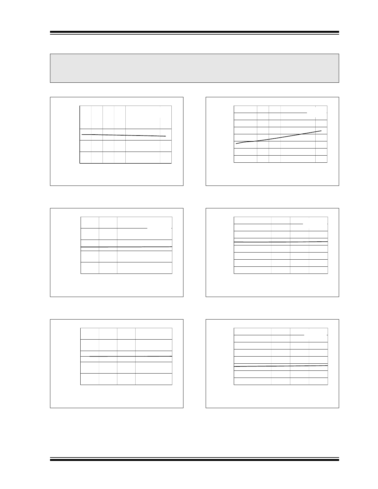
2.0
TYPICAL PERFORMANCE CURVES
NOTE: Unless otherwise indicated, V
DD
= [V
REG
(Typ) + 1V], I
OUT
= 10 mA and T
A
= +25°C.
FIGURE 2-1:
Battery Regulation Voltage
(V
BAT
) vs. Charge Current (I
OUT
).
FIGURE 2-2:
Battery Regulation Voltage
(V
BAT
) vs. Supply Voltage (V
DD
).
FIGURE 2-3:
Battery Regulation Voltage
(V
BAT
) vs. Supply Voltage (V
DD
).
FIGURE 2-4:
Supply Current (I
SS
) vs.
Charge Current (I
OUT
).
FIGURE 2-5:
Supply Current (I
SS
) vs.
Supply Voltage (V
DD
).
FIGURE 2-6:
Supply Current (I
SS
) vs.
Supply Voltage (V
DD
).
NOTE: Unless otherwise indicated, V
DD
= [V
REG
(Typ) + 1V], I
OUT
= 10 mA and T
A
= +25°C.
Note:
The graphs and tables provided following this note are a statistical summary based on a limited number of
samples and are provided for informational purposes only. The performance characteristics listed herein
are not tested or guaranteed. In some graphs or tables, the data presented may be outside the specified
operating range (e.g., outside specified power supply range) and therefore outside the warranted range.
4.150
4.170
4.190
4.210
4.230
4.250
0
50
100 150 200 250 300 350 400
I
OUT
(mA)
V
BA
T
(V
)
V
SET
= V
DD
V
DD
= 5.2 V
4.150
4.170
4.190
4.210
4.230
4.250
4.5
4.7
4.9
5.1
5.3
5.5
V
DD
(V)
V
BA
T
(V
)
V
SET
= V
DD
I
OUT
= 375 mA
4.150
4.170
4.190
4.210
4.230
4.250
4.5
4.7
4.9
5.1
5.3
5.5
V
DD
(V)
V
BA
T
(V
)
V
SET
= V
DD
I
OUT
= 10 mA
0.20
0.30
0.40
0.50
0.60
0.70
0.80
0.90
1.00
0
50
100 150 200 250 300 350 400
I
OUT
(mA)
I
SS
(mA)
V
SET
= V
DD
V
DD
= 5.2 V
0.20
0.30
0.40
0.50
0.60
0.70
0.80
0.90
1.00
4.5
4.7
4.9
5.1
5.3
5.5
V
DD
(V)
I
SS
(m
A)
V
SET
= V
DD
I
OUT
= 375 mA
0.20
0.30
0.40
0.50
0.60
0.70
0.80
0.90
1.00
4.5
4.7
4.9
5.1
5.3
5.5
V
DD
(V)
I
SS
(mA)
V
SET
= V
DD
I
OUT
= 10 mA
MCP73853/55
DS21915C-page 8
2004-2013 Microchip Technology Inc.
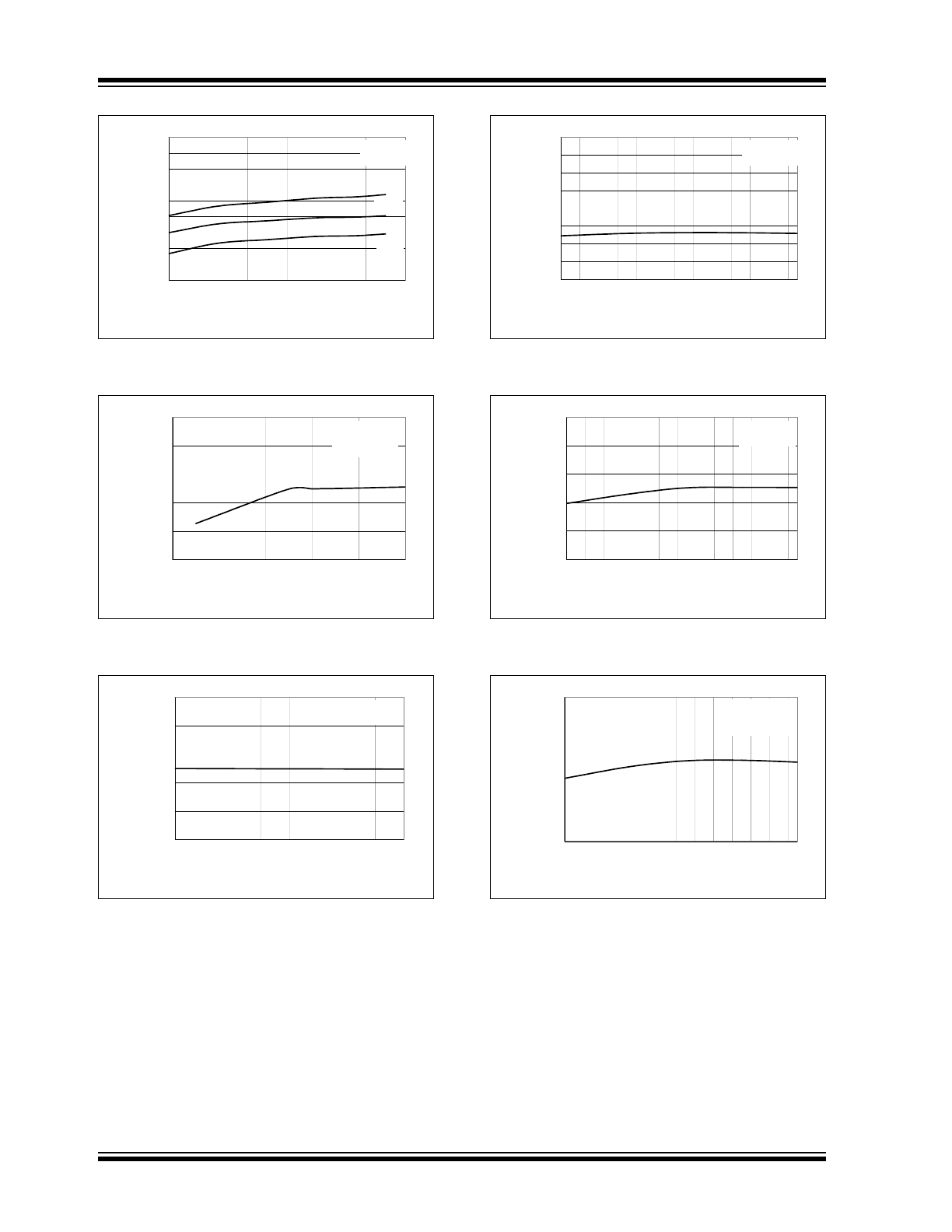
FIGURE 2-7:
Output Leakage Current
(I
DISCHARGE
) vs. Battery Voltage (V
BAT
).
FIGURE 2-8:
Thermistor Reference
Voltage (V
THREF
) vs. Supply Voltage (V
DD
).
FIGURE 2-9:
Thermistor Reference
Voltage (V
THREF
) vs. Thermistor Bias Current
(I
THREF
).
FIGURE 2-10:
Supply Current (I
SS
) vs.
Ambient Temperature (T
A
).
FIGURE 2-11:
Battery Regulation Voltage
(V
BAT
) vs. Ambient Temperature (T
A
).
FIGURE 2-12:
Thermistor Reference
Voltage (V
THREF
) vs. Ambient Temperature (T
A
).
NOTE: Unless otherwise indicated, V
DD
= [V
REG
(Typ) + 1V], I
OUT
= 10 mA and T
A
= +25°C.
0.00
0.05
0.10
0.15
0.20
0.25
0.30
0.35
0.40
0.45
2.0
2.4
2.8
3.2
3.6
4.0
4.4
V
BAT
(V)
I
D
IS
C
HA
RGE
(mA
)
V
SET
= V
DD
V
DD
= V
SS
+25°C
-40°C
+85°C
2.525
2.535
2.545
2.555
2.565
2.575
4.5
4.7
4.9
5.1
5.3
5.5
V
DD
(V)
V
T
HRE
F
(V
)
MCP73853
V
SET
= V
DD
I
THREF
= 100 µA
2.525
2.535
2.545
2.555
2.565
2.575
0
25
50
75
100 125 150 175 200
I
THREF
(µA)
V
TH
R
E
F
(V
)
MCP73853
V
SET
= V
DD
0.20
0.30
0.40
0.50
0.60
0.70
0.80
0.90
1.00
-4
0
-3
0
-2
0
-1
0
0
10
20
30
40
50
60
70
80
T
A
(°C)
I
SS
(m
A)
V
SET
= V
DD
I
OUT
= 10 mA
4.150
4.170
4.190
4.210
4.230
4.250
-4
0
-3
0
-2
0
-1
0
0
10
20
30
40
50
60
70
80
T
A
(°C)
V
BAT
(V
)
V
SET
= V
DD
I
OUT
= 10 mA
2.525
2.535
2.545
2.555
2.565
2.575
-4
0
-3
0
-2
0
-1
0
0
10
20
30
40
50
60
70
80
T
A
(°C)
V
T
HRE
F
(V
)
MCP73853
V
SET
= V
DD
I
THREF
= 100 µA
2004-2013 Microchip Technology Inc.
DS21915C-page 9
MCP73853/55
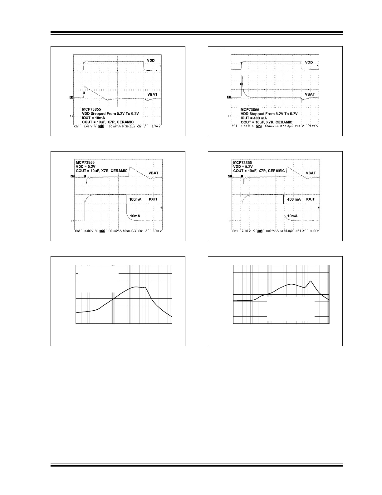
FIGURE 2-13:
Line Transient Response.
FIGURE 2-14:
Load Transient Response.
FIGURE 2-15:
Power Supply Ripple
Rejection.
FIGURE 2-16:
Line Transient Response.
FIGURE 2-17:
Load Transient Response.
FIGURE 2-18:
Power Supply Ripple
Rejection.
NOTE: Unless otherwise indicated, V
DD
= [V
REG
(Typ) + 1V], I
OUT
= 10 mA, and T
A
= +25°C.
-70
-60
-50
-40
-30
-20
-10
0
0.01
0.1
1
10
100
1000
Frequency (kHz)
A
tte
nua
ti
on (dB
)
MCP73853
V
DD
= 5.2 V
V
AC
= 100 mVp-p
I
OUT
= 10 mA
C
OUT
= 10
F, Ceramic
-80
-70
-60
-50
-40
-30
-20
-10
0
0.01
0.1
1
10
100
1000
Frequency (kHz)
At
ten
u
at
io
n (d
B)
MCP73853
V
DD
= 5.2 V
V
AC
= 100 mVp-p
I
OUT
= 100 mA
C
OUT
= 10
F, X7R, Ceramic
MCP73853/55
DS21915C-page 10
2004-2013 Microchip Technology Inc.
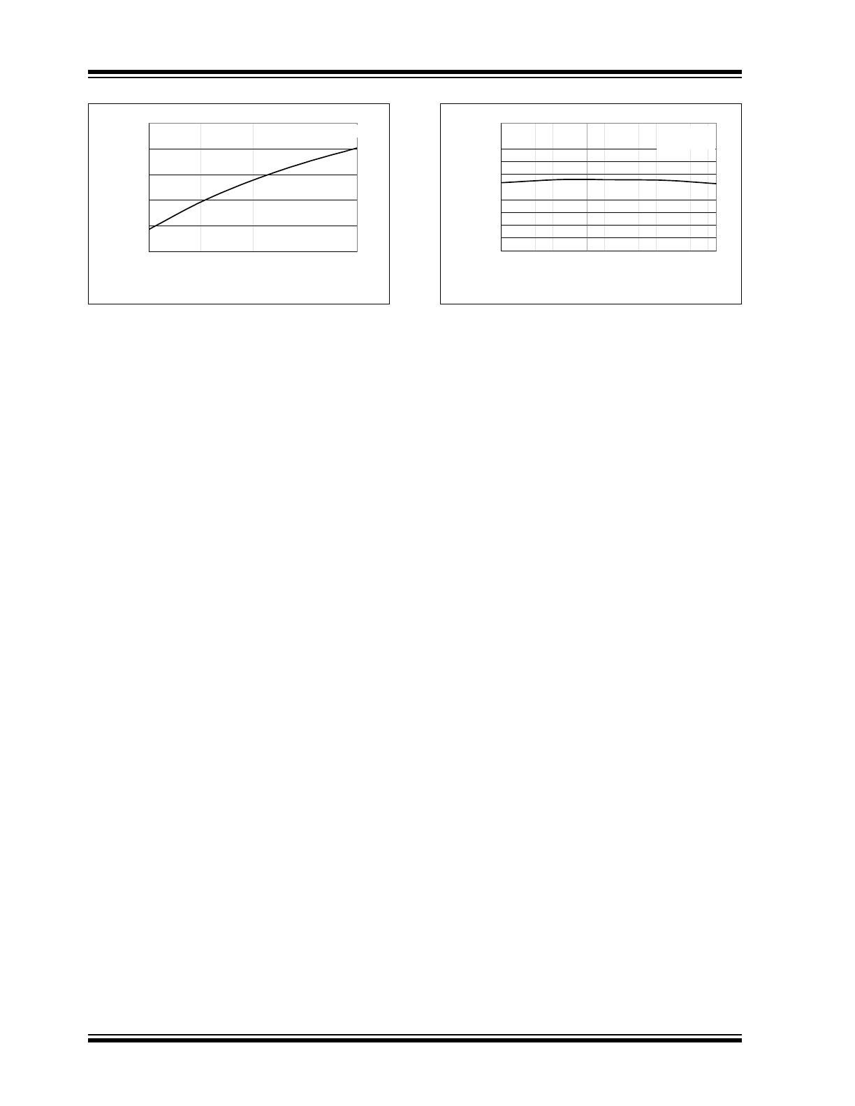
FIGURE 2-19:
Charge Current (I
OUT
) vs.
Programming Resistor (R
PROG
).
FIGURE 2-20:
Charge Current (I
OUT
) vs.
Ambient Temperature (T
A
).
0
100
200
300
400
500
OPEN
4.8K
1.6K
536
0
R
PROG
()
I
OU
T
(m
A)
V
SET
= V
DD
250
255
260
265
270
275
280
285
290
295
300
-4
0
-3
0
-2
0
-1
0
0
10
20
30
40
50
60
70
80
T
A
(°C)
I
OUT
(mA
)
V
SET
= V
DD
R
PROG
= 1.6 k