
2008-2016 Microchip Technology Inc.
DS20002092G-page
1
MCP1415/16
Features
• High Peak Output Current: 1.5A (typical)
• Wide Input Supply Voltage Operating Range:
- 4.5V to 18V
• Low Shoot-Through/Cross-Conduction Current in
Output Stage
• High Capacitive Load Drive Capability:
- 470
pF in 13
ns (typical)
- 1000
pF in 18
ns (typical)
• Short Delay Times: 44
ns (t
D1
), 47
ns (MCP1415
t
D2
), 54
ns (MCP1416 t
D2
) (typical)
• Low Supply Current:
- With Logic ‘1’ Input - 0.65
mA (typical)
- With Logic ‘0’ Input - 0.1
mA (typical)
• Latch-Up Protected: Withstands 500
mA Reverse
Current
• Logic Input Withstands Negative Swing up to 5V
• Space-Saving 5L SOT-23 Package
Applications
• Switch Mode Power Supplies
• Pulse Transformer Drive
• Line Drivers
• Level Translator
• Motor and Solenoid Drive
General Description
The MCP1415/16 devices are high-speed, dual
MOSFET drivers that are capable of providing up to
1.5A of peak current while operating from a single 4.5V
to 18V supply. The inverting or non-inverting single
channel output is directly controlled from either TTL or
CMOS (3V to 18V) logic. These devices also feature
low shoot-through current, matched rise and fall time,
and short propagation delays which make them ideal
for high switching frequency applications. They provide
low enough impedances in both the ‘On’ and ‘Off’
states to ensure the intended state of the MOSFET is
not affected, even by large transients.
These devices are highly latch-up resistant under any
condition within their power and voltage ratings. They
are not subject to damage when noise spiking (up to
5V, of either polarity) occurs on the Ground pin. They
can accept up to 500 mA of reverse current being
forced back into their outputs without damage or logic
upset. All terminals are fully protected against
electrostatic discharge (ESD) up to 2.0
kV (HBM) and
300V (MM).
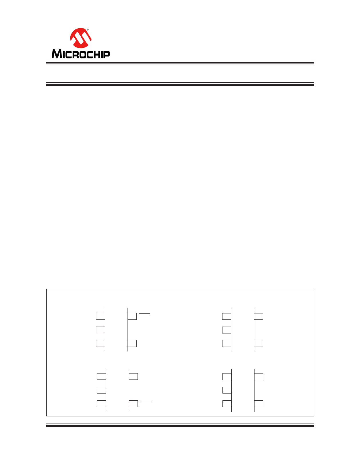
Package Types
4
1
2
3
5
4
1
2
3
5
4
1
2
3
5
4
1
2
3
5
V
DD
NC
IN
V
DD
NC
IN
NC
IN
GND
NC
IN
GND
SOT-23-5
MCP1415
MCP1416
MCP1415R
MCP1416R
OUT
GND
OUT
GND
V
DD
OUT
OUT
V
DD
Tiny 1.5A, High-Speed Power MOSFET Driver
MCP1415/16
DS20002092G-page
2
2008-2016 Microchip Technology Inc.
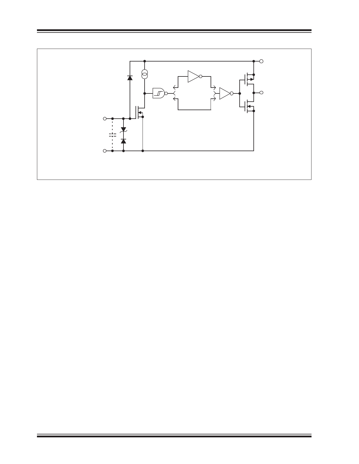
Functional Block Diagram
Effective
Input C = 25 pF
Input
GND
V
DD
300 mV
4.7V
Inverting
Non-inverting
Note:
Unused inputs should be grounded.
650 μA
Output
(Each Input)
MCP1415
Inverting
MCP1416
Non-inverting
2008-2016 Microchip Technology Inc.
DS20002092G-page
3
MCP1415/16
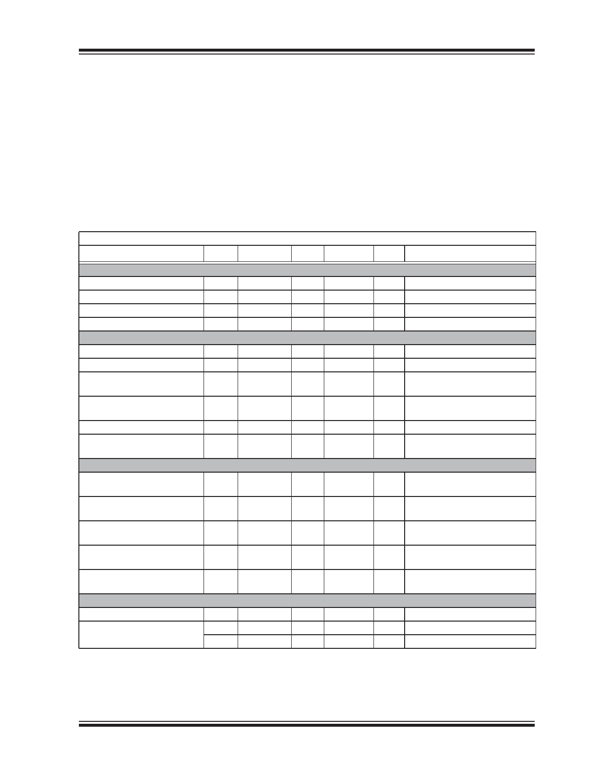
1.0
ELECTRICAL
CHARACTERISTICS
Absolute Maximum Ratings †
V
DD
, Supply Voltage.............................................+20V
V
IN
, Input Voltage..............(V
DD
+
0.3V)
to
(GND
- 5V)
Package Power Dissipation (T
A
=
50°C)
5L SOT23......................................................0.39W
ESD Protection on all Pins ......................2.0
kV (HBM)
................................................................... 300V (MM)
† Notice:
Stresses above those listed under “Maximum
Ratings” may cause permanent damage to the device.
This is a stress rating only and functional operation of
the device at those or any other conditions above those
indicated in the operational sections of this
specification is not intended. Exposure to maximum
rating conditions for extended periods may affect
device reliability.
DC CHARACTERISTICS
Electrical Specifications:
Unless otherwise noted, T
A
=
+25°C, with 4.5V
V
DD
18V
Parameters
Sym.
Min.
Typ.
Max.
Units
Conditions
Input
Logic ‘1’ High Input Voltage
V
IH
2.4
1.9
—
V
Logic ‘0’ Low Input Voltage
V
IL
—
1.6
0.8
V
Input Current
I
IN
-1
—
+1
μA
0V
V
IN
V
DD
Input Voltage
V
IN
-5
—
V
DD
+
0.3
V
Output
High Output Voltage
V
OH
V
DD
- 0.025
—
—
V
DC Test
Low Output Voltage
V
OL
—
—
0.025
V
DC Test
Output Resistance, High
R
OH
—
6
7.5
I
OUT
=
10
mA, V
DD
=
18V
(
Note
1
)
Output Resistance, Low
R
OL
—
4
5.5
I
OUT
=
10
mA, V
DD
=
18V
(
Note
1
)
Peak Output Current
I
PK
—
1.5
—
A
V
DD
=
18V (
Note
1
)
Latch-Up Protection Withstand
Reverse Current
I
REV
0.5
—
—
A
Duty cycle
2%, t 300
μs
(
Note
1
)
Switching Time (
Note
1
)
Rise Time
t
R
—
18
25
ns
V
DD
=
18V, C
L
=
1000
pF
Figure
4-1
,
Figure
4-2
(
Note
1
)
Fall Time
t
F
—
21
28
ns
V
DD
=
18V, C
L
=
1000
pF
Figure
4-1
,
Figure
4-2
(
Note
1
)
Delay Time
t
D1
—
44
54
ns
V
DD
=
18V, V
IN
=
5V
Figure
4-1
,
Figure
4-2
(
Note
1
)
MCP1415 Delay Time
t
D2
—
47
57
ns
V
DD
=
18V, V
IN
=
5V
Figure
4-1
(
Note
1
)
MCP1416 Delay Time
t
D2
—
54
64
ns
V
DD
=
18V, V
IN
=
5V
Figure
4-2
(
Note
1
)
Power Supply
Supply Voltage
V
DD
4.5
—
18
V
Power Supply Current
I
S
—
0.65
1.1
mA
V
IN
=
3V
I
S
—
0.1
0.15
mA
V
IN
=
0V
Note 1:
Tested during characterization, not production tested.
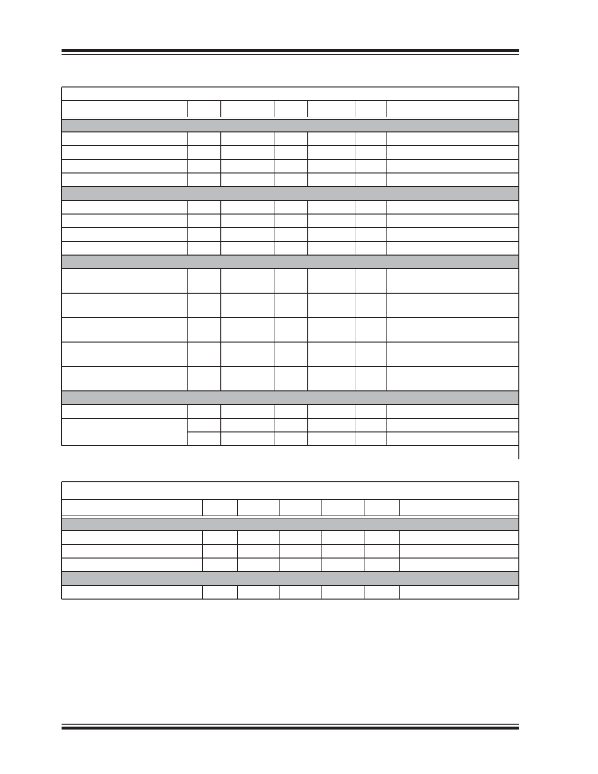
DC CHARACTERISTICS (OVER OPERATING TEMPERATURE RANGE) (
Note
1
)
Electrical Specifications:
Unless otherwise indicated, over the operating range with 4.5V
V
DD
18V.
Parameters
Sym.
Min.
Typ.
Max.
Units
Conditions
Input
Logic ‘1’, High Input Voltage
V
IH
2.4
—
—
V
Logic ‘0’, Low Input Voltage
V
IL
—
—
0.8
V
Input Current
I
IN
-10
—
+10
μA
0V
V
IN
V
DD
Input Voltage
V
IN
-5
—
V
DD
+
0.3
V
Output
High Output Voltage
V
OH
V
DD
- 0.025
—
—
V
DC Test
Low Output Voltage
V
OL
—
—
0.025
V
DC Test
Output Resistance, High
R
OH
—
8.5
9.5
I
OUT
=
10
mA, V
DD
=
18V
Output Resistance, Low
R
OL
—
6
7
I
OUT
=
10
mA, V
DD
=
18V
Switching Time
Rise Time
t
R
—
26
37
ns
V
DD
=
18V, C
L
=
1000
pF
Figure
4-1
,
Figure
4-2
Fall Time
t
F
—
29
40
ns
V
DD
=
18V, C
L
=
1000
pF
Figure
4-1
,
Figure
4-2
Delay Time
t
D1
—
60
70
ns
V
DD
=
18V, V
IN
=
5V
Figure
4-1
,
Figure
4-2
MCP1415 Delay Time
t
D2
—
62
72
ns
V
DD
=
18V, V
IN
=
5V
Figure
4-1
MCP1416 Delay Time
t
D2
—
72
82
ns
V
DD
=
18V, V
IN
=
5V
Figure
4-2
Power Supply
Supply Voltage
V
DD
4.5
—
18
V
Power Supply Current
I
S
—
0.75
1.5
mA
V
IN
=
3.0V
I
S
—
0.15
0.25
mA
V
IN
=
0V
Note 1:
Tested during characterization, not production tested.
TEMPERATURE CHARACTERISTICS
Electrical Specifications:
Unless otherwise noted, all parameters apply with 4.5V
V
DD
18V
Parameter
Sym.
Min.
Typ.
Max.
Units
Comments
Temperature Ranges
Specified Temperature Range
T
A
-40
—
+125
°C
Maximum Junction Temperature
T
J
—
—
+150
°C
Storage Temperature Range
T
A
-65
—
+150
°C
Package Thermal Resistances
Thermal Resistance, 5LD SOT23
JA
—
220.7
—
°C/W
MCP1415/16
DS20002092G-page
4
2008-2016 Microchip Technology Inc.
2008-2016 Microchip Technology Inc.
DS20002092G-page
5
MCP1415/16
2.0
TYPICAL PERFORMANCE CURVES
Note:
The graphs and tables provided following this note are a statistical summary based on a limited number of
samples and are provided for informational purposes only. The performance characteristics listed herein are
not tested or guaranteed. In some graphs or tables, the data presented may be outside the specified
operating range (e.g., outside specified power supply range) and therefore outside the warranted range.
Note:
Unless otherwise indicated, T
A
=
+25°C with 4.5V
V
DD
= 18V.
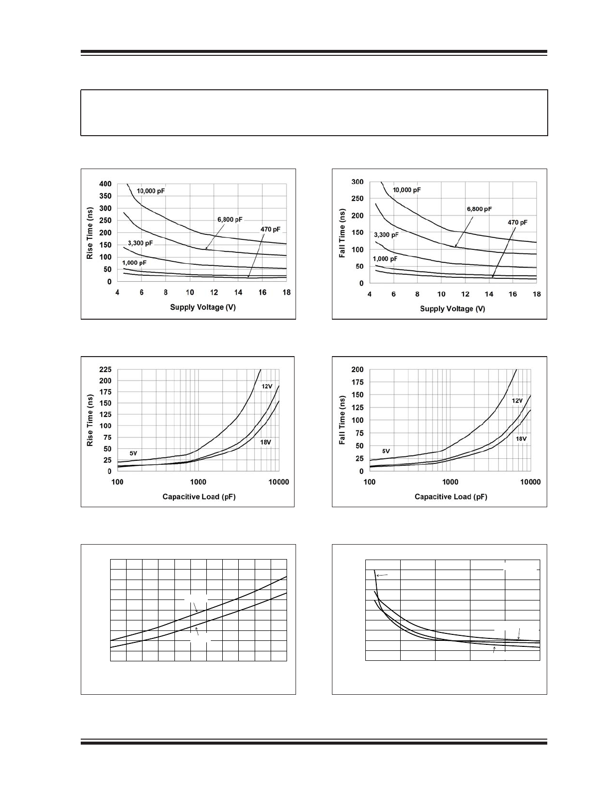
FIGURE 2-1:
Rise Time vs. Supply
Voltage.
FIGURE 2-2:
Rise Time vs. Capacitive
Load.
12
14
16
18
20
22
24
26
28
30
32
-40 -25 -10
5
20
35
50
65
80
95 110 125
T
ime (ns)
Temperature (
°C)
t
RISE
t
FALL
FIGURE 2-3:
Rise and Fall Times vs.
Temperature.
FIGURE 2-4:
Fall Time vs. Supply
Voltage.
FIGURE 2-5:
Fall Time vs. Capacitive
Load.
20
30
40
50
60
70
80
90
100
110
120
2
4
6
8
10
12
Propagation Delay
(ns)
Input Amplitude (V)
t
D1
MCP1415
t
D2
MCP1416
t
D2
V
DD
= 18V
FIGURE 2-6:
Propagation Delay Time vs.
Input Amplitude.
MCP1415/16
DS20002092G-page
6
2008-2016 Microchip Technology Inc.
Note:
Unless otherwise indicated, T
A
=
+25°C with 4.5V
V
DD
= 18V.
20
30
40
50
60
70
80
90
100
110
120
130
140
4
6
8
10
12
14
16
18
Propagation Delay
(ns)
Supply Voltage(V)
t
D1
MCP1415
t
D2
MCP1416 t
D2
V
IN
= 5V
FIGURE 2-7:
Propagation Delay Time vs.
Supply Voltage.
20
30
40
50
60
70
80
-40 -25 -10
5
20
35
50
65
80
95 110 125
Propagation Delay
(ns)
Temperature (
°C)
t
D1
MCP1415 t
D2
MCP1416 t
D2
V
IN
= 5V
V
DD
= 18V
FIGURE 2-8:
Propagation Delay Time vs.
Temperature.
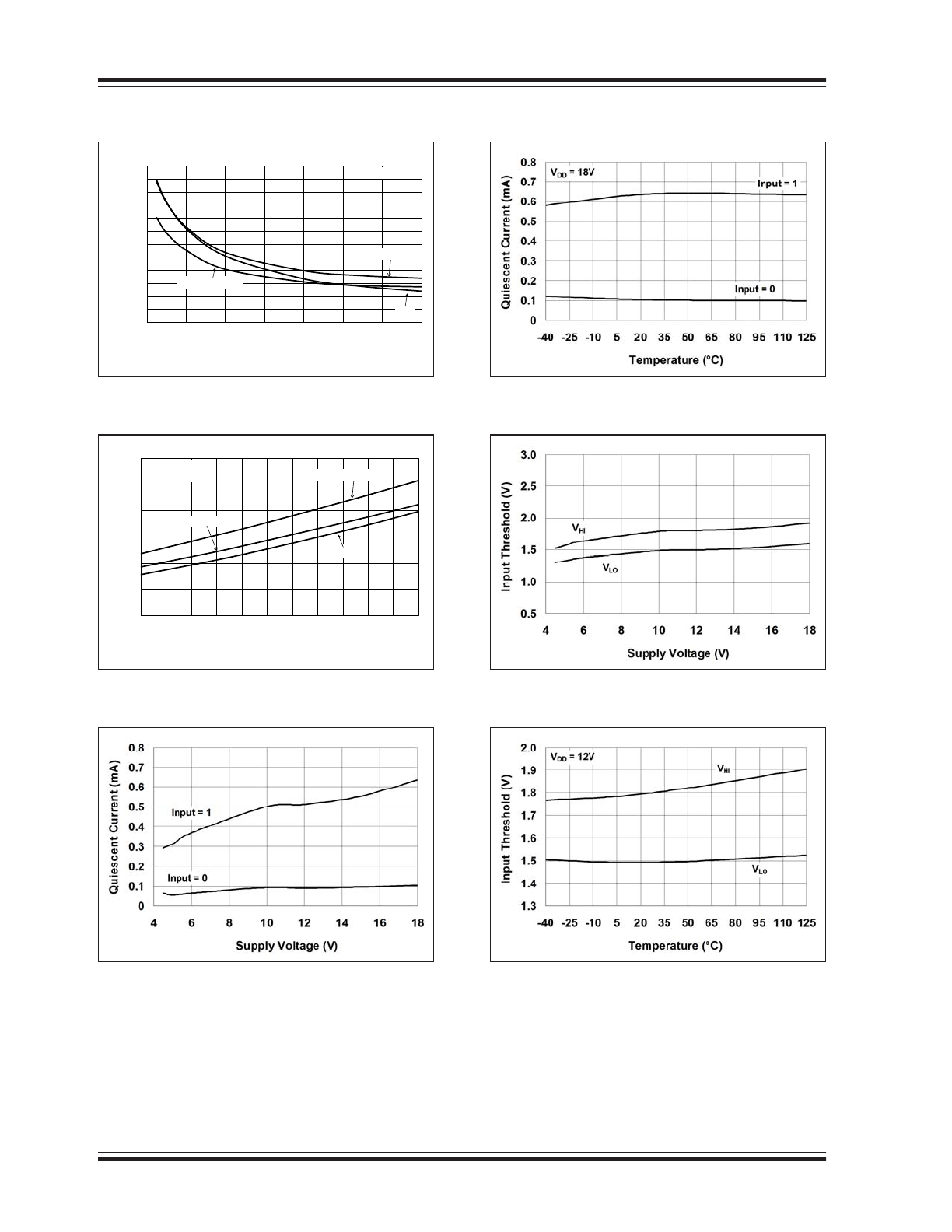
FIGURE 2-9:
Quiescent Current vs.
Supply Voltage.
FIGURE 2-10:
Quiescent Current vs.
Temperature.
FIGURE 2-11:
Input Threshold vs. Supply
Voltage.
FIGURE 2-12:
Input Threshold vs.
Temperature.
2008-2016 Microchip Technology Inc.
DS20002092G-page
7
MCP1415/16
Note:
Unless otherwise indicated, T
A
=
+25°C with 4.5V
V
DD
= 18V.
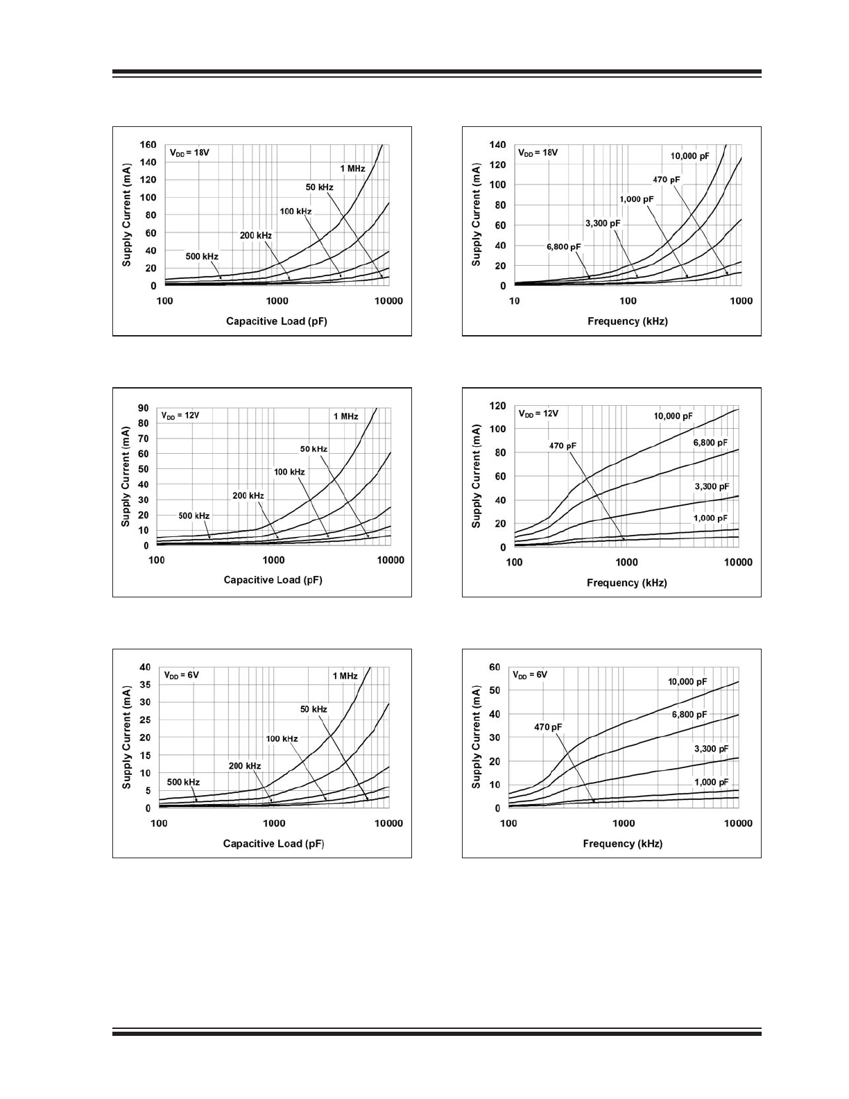
FIGURE 2-13:
Supply Current vs.
Capacitive Load.
FIGURE 2-14:
Supply Current vs.
Capacitive Load.
FIGURE 2-15:
Supply Current vs.
Capacitive Load.
FIGURE 2-16:
Supply Current vs.
Frequency.
FIGURE 2-17:
Supply Current vs.
Frequency.
FIGURE 2-18:
Supply Current vs.
Frequency.
MCP1415/16
DS20002092G-page
8
2008-2016 Microchip Technology Inc.
Note:
Unless otherwise indicated, T
A
=
+25°C with 4.5V
V
DD
= 18V.
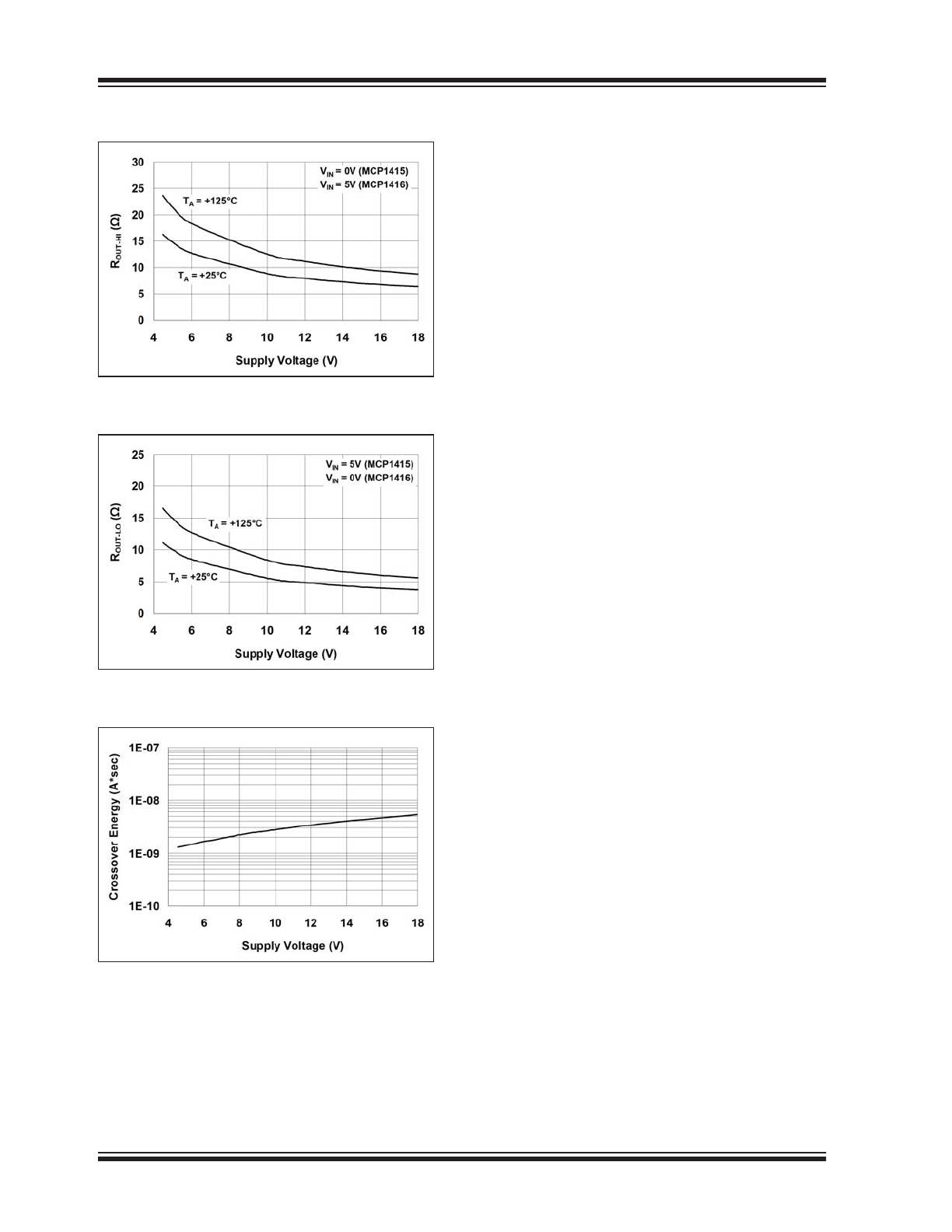
FIGURE 2-19:
Output Resistance (Output
High) vs. Supply Voltage.
FIGURE 2-20:
Output Resistance (Output
Low) vs. Supply Voltage.
FIGURE 2-21:
Crossover Energy vs.
Supply Voltage.
2008-2016 Microchip Technology Inc.
DS20002092G-page
9
MCP1415/16
3.0
PIN DESCRIPTIONS
The descriptions of the pins are listed in
Table
3-1
.
TABLE 3-1:
PIN FUNCTION TABLE
Pin No.
Symbol
Description
MCP1415/16
MCP1415R/16R
1
1
NC
No Connection
2
5
V
DD
Supply Input
3
3
IN
Control Input
4
2
GND
Ground
5
4
OUT/OUT
Output
3.1
Supply Input (V
DD
)
V
DD
is the bias supply input for the MOSFET driver and
has a voltage range of 4.5V to 18V. This input must be
decoupled to ground with a local capacitor. This bypass
capacitor provides a localized low-impedance path for
the peak currents that are provided to the load.
3.2
Control Input (IN)
The MOSFET driver input is a high-impedance,
TTL/CMOS compatible input. The input also has
hysteresis between the high and low input levels,
allowing them to be driven from slow rising and falling
signals and to provide noise immunity.
3.3
Ground (GND)
Ground is the device return pin. The ground pin should
have a low-impedance connection to the bias supply
source return. When the capacitive load is being
discharged, high peak currents will flow out of the
ground pin.
3.4
Output (OUT, OUT)
The output is a CMOS push-pull output that is capable
of sourcing and sinking 1.5A of peak current
(V
DD
=
18V). The low output impedance ensures the
gate of the external MOSFET stays in the intended
state even during large transients. This output also has
a reverse current latch-up rating of 500
mA.
MCP1415/16
DS20002092G-page
10
2008-2016 Microchip Technology Inc.
4.0
APPLICATION INFORMATION
4.1
General Information
MOSFET drivers are high-speed, high-current devices
which are intended to source/sink high peak currents to
charge/discharge the gate capacitance of external
MOSFETs or Insulated-Gate Bipolar Transistors
(IGBTs). In high frequency switching power supplies,
the Pulse-Width Modulation (PWM) controller may not
have the drive capability to directly drive the power
MOSFET. A MOSFET driver such as the MCP1415/16
family can be used to provide additional source/sink
current capability.
4.2
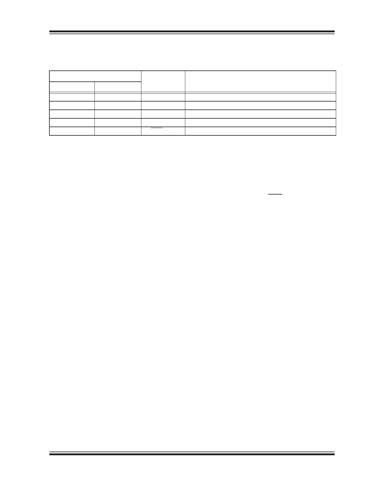
MOSFET Driver Timing
The ability of a MOSFET driver to transition from a
fully-off state to a fully-on state is characterized by the
driver’s rise time (t
R
), fall time (t
F
) and propagation
delays (t
D1
and t
D2
).
Figure
4-1
and
Figure
4-2
show
the test circuit and timing waveform used to verify the
MCP1415/16 timing.
0.1 μF
+5V
10%
90%
10%
90%
10%
90%
18V
1 μF
0V
0V
C
L
= 1000 pF
Input
Input
Output
t
D1
t
F
t
D2
Output
t
R
V
DD
= 18V
Ceramic
MCP1415
Note:
Input Signal: t
RISE
=
t
FALL
≤ 10
ns
100
Hz, 0-5V Square Wave
FIGURE 4-1:
Inverting Driver Timing
Waveform.
90%
Input
t
D1
t
F
t
D2
Output
t
R
10%
10%
10%
+5V
18V
0V
0V
90%
90%
0.1 μF
1 μF
C
L
= 1000 pF
Input
Output
V
DD
= 18V
Ceramic
MCP1416
Note:
Input Signal: t
RISE
=
t
FALL
≤ 10
ns
100
Hz, 0-5V Square Wave
FIGURE 4-2:
Non-Inverting Driver Timing
Waveform.
4.3
Decoupling Capacitors
Careful layout and decoupling capacitors are required
when using power MOSFET drivers. Large current is
required to charge and discharge capacitive loads
quickly. For example, approximately 720
mA are
needed to charge a 1000
pF load with 18V in 25
ns.
To operate the MOSFET driver over a wide frequency
range with low supply impedance, it is recommended to
place a ceramic and a low ESR film capacitor in parallel
between the driver V
DD
and GND. A 1.0
μF low ESR
film capacitor and a 0.1
μF ceramic capacitor placed
between pins 2 and 4 are required for reliable
operation. These capacitors should be placed close to
the driver to minimize circuit board parasitics and
provide a local source for the required current.