

Features
•
Utilizes the ARM7TDMI
®
ARM
®
Thumb
®
Processor Core
– High-performance 32-bit RISC Architecture
– High-density 16-bit Instruction Set
– Leader in MIPS/Watt
– Embedded ICE (In-circuit Emulation)
•
8K Bytes Internal SRAM
•
Fully Programmable External Bus Interface (EBI)
– Maximum External Address Space of 64M Bytes
– Up to 8 Chip Selects
– Software Programmable 8/16-bit External Data Bus
•
8-channel Peripheral Data Controller
•
8-level Priority, Individually Maskable, Vectored Interrupt Controller
– 5 External Interrupts, Including a High-priority, Low-latency Interrupt Request
•
54 Programmable I/O Lines
•
6-channel 16-bit Timer/Counter
– 6 External Clock Inputs, 2 Multi-purpose I/O Pins per Channel
•
2 USARTs
– 2 Dedicated Peripheral Data Controller (PDC) Channels per USART
– Support for up to 9-bit Data Transfers
•
2 Master/Slave SPI Interfaces
– 2 Dedicated Peripheral Data Controller (PDC) Channels per SPI
– 8- to 16-bit Programmable Data Length
– 4 External Slave Chip Selects per SPI
•
3 System Timers:
– Period Interval Timer (PIT); Real-time Timer (RTT); Watchdog Timer (WDT)
•
Power Management Controller (PMC)
– CPU and Peripherals Can be Deactivated Individually
•
Clock Generator with 32.768 kHz Low-power Oscillator and PLL
– Support for 38.4 kHz Crystals
– Software Programmable System Clock (up to 33 MHz)
•
IEEE
®
1149.1 JTAG Boundary Scan on All Active Pins
•
Fully Static Operation: 0 Hz to 33 MHz Internal Frequency Range
at VDDCORE = 3.0V, 85
°
C
•
2.7V to 3.6V Core and PLL Operating Voltage Range; 2.7V to 5.5V I/O Operating Voltage
Range
•
-40
°
C to +85
°
C Temperature Range
•
Available in a 144-lead LQFP Package (Green) and a 144-ball BGA Package (RoHS-
compliant)
1.
Description
The AT91M42800A is a member of the Atmel AT91 16/32-bit microcontroller family,
which is based on the ARM7TDMI processor core. This processor has a high-perfor-
mance 32-bit RISC architecture with a high-density 16-bit instruction set and very low
power consumption. In addition, a large number of internally banked registers result in
very fast exception handling, making the device ideal for real-time control applica-
tions. The AT91 ARM-based MCU family also features Atmel’s high-density, in-
system programmable, nonvolatile memory technology. The AT91M42800A has a
direct connection to off-chip memory, including Flash, through the External Bus
Interface.
AT91
ARM Thumb
Microcontrollers
AT91M42800A
Summary
Rev. 1779ES–ATARM–14-Apr-06
Note: This is a summary document. A complete document is
available on our web site at www.atmel.com.
2
1779ES–ATARM–14-Apr-06
AT91M42800A
The Power Management Controller allows the user to adjust device activity according to system
requirements, and, with the 32.768 kHz low-power oscillator, enables the AT91M42800A to
reduce power requirements to an absolute minimum. The AT91M42800A is manufactured using
Atmel’s high-density CMOS technology. By combining the ARM7TDMI processor core with on-
chip SRAM and a wide range of peripheral functions including timers, serial communication con-
trollers and a versatile clock generator on a monolithic chip, the AT91M42800A provides a
highly-flexible and cost-effective solution to many compute-intensive applications.
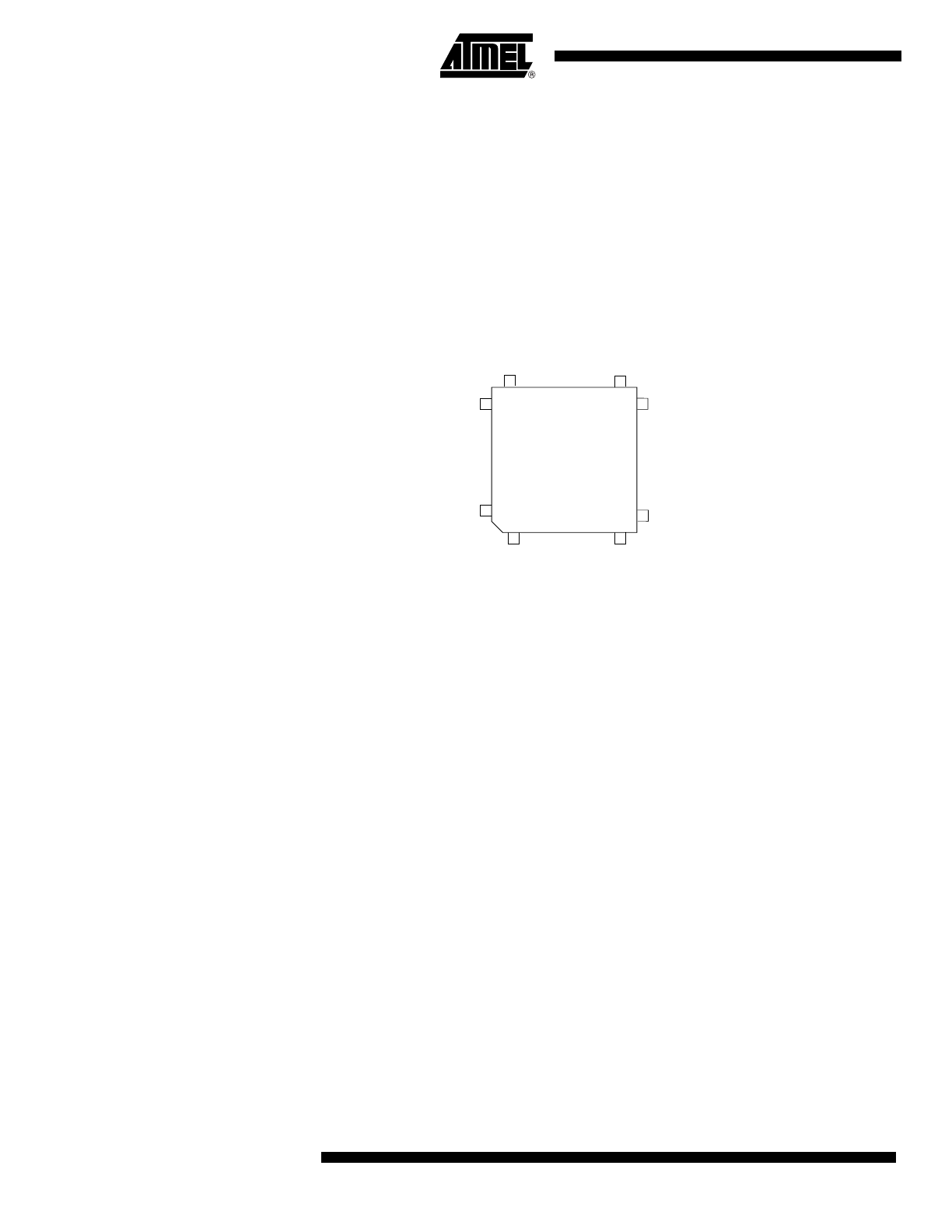
2.
Pin Configuration
Figure 2-1.
Pin Configuration in LQFP144 Package (Top View)
1
36
144
109
108
73
37
72
AT91M42800 33AI
3
1779ES–ATARM–14-Apr-06
AT91M42800A
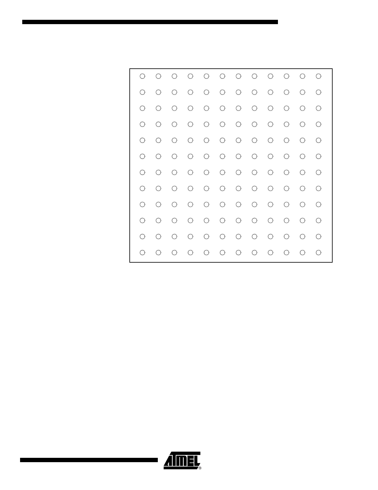
Figure 2-2.
Pin Configuration in BGA144 Package (Top View)
1
2
3
4
5
6
7
8
9
10
11
12
A
B
C
D
E
F
G
H
J
K
L
M

4
1779ES–ATARM–14-Apr-06
AT91M42800A
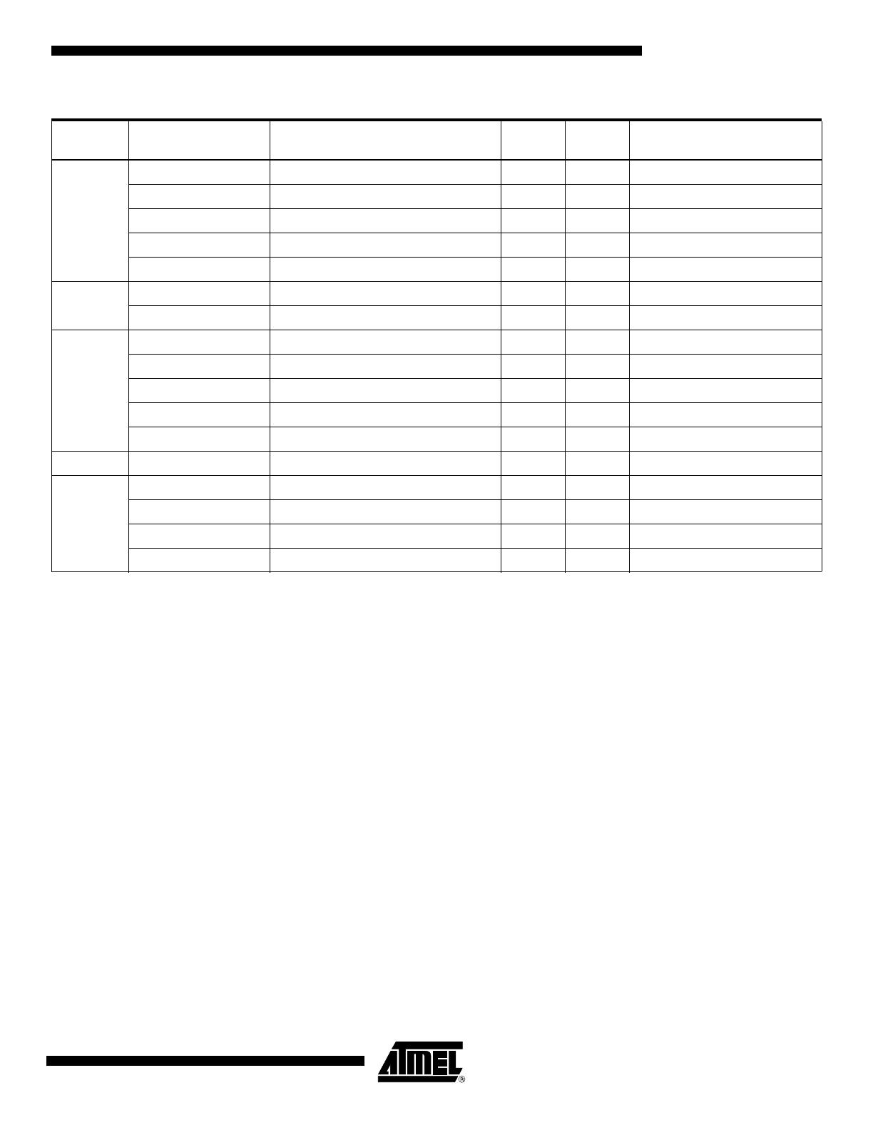
Table 2-1.
AT91M42800A Pinout in LQFP 144 Package
Pin#
Name
Pin#
Name
Pin#
Name
Pin#
Name
1
GND
37
GND
73
GND
109
GND
2
GND
38
GND
74
GND
110
GND
3
NLB/A0
39
D4
75
PB22/TIOA5
111
PA26
4
A1
40
D5
76
PB23/TIOB5
112
MODE0
5
A2
41
D6
77
PA0/IRQ0
113
XIN
6
A3
42
D7
78
PA1/IRQ1
114
XOUT
7
A4
43
D8
79
PA2/IRQ2
115
GND
8
A5
44
D9
80
PA3/IRQ3
116
PLLRCA
9
A6
45
D10
81
PA4/FIQ
117
VDDPLL
10
A7
46
D11
82
PA5/SCK0
118
PLLRCB
11
A8
47
D12
83
PA6/TXD0
119
VDDPLL
12
VDDIO
48
VDDIO
84
VDDIO
120
VDDIO
13
GND
49
GND
85
GND
121
GND
14
A9
50
D13
86
PA7/RXD0
122
NWDOVF
15
A10
51
D14
87
PA8/SCK1
123
PA27/BMS
16
A11
52
D15
88
PA9/TXD1/NTRI
124
MODE1
17
A12
53
PB6/TCLK0
89
PA10/RXD1
125
TMS
18
A13
54
PB7/TIOA0
90
PA11/SPCKA
126
TDI
19
A14
55
PB8/TIOB0
91
PA12/MISOA
127
TDO
20
A15
56
PB9/TCLK1
92
PA13/MOSIA
128
TCK
21
A16
57
PB10/TIOA1
93
PA14/NPCSA0/NSSA
129
NTRST
22
A17
58
PB11/TIOB1
94
PA15/NPCSA1
130
NRST
23
A18
59
PB12/TCLK2
95
PA16/NPCSA2
131
PA28
24
VDDIO
60
VDDIO
96
VDDIO
132
VDDIO
25
GND
61
GND
97
GND
133
GND
26
A19
62
PB13/TIOA2
98
PA17/NPCSA3
134
PA29/PME
27
PB2/A20/CS7
63
PB14/TIOB2
99
PA18/SPCKB
135
NWAIT
28
PB3/A21/CS6
64
PB15/TCLK3
100
PA19/MISOB
136
NOE/NRD
29
PB4/A22/CS5
65
PB16/TIOA3
101
PA20/MOSIB
137
NWE/NWR0
30
PB5/A23/CS4
66
PB17/TIOB3
102
PA21/NPCSB0/NSSB
138
NUB/NWR1
31
D0
67
PB18/TCLK4
103
PA22/NPCSB1
139
NCS0
32
D1
68
PB19/TIOA4
104
PA23/NPCSB2
140
NCS1
33
D2
69
PB20/TIOB4
105
PA24/NPCSB3
141
PB0/NCS2
34
D3
70
PB21/TCLK5
106
PA25/MCKO
142
PB1/NCS3
35
VDDCORE
71
VDDCORE
107
VDDCORE
143
VDDCORE
36
VDDIO
72
VDDIO
108
VDDIO
144
VDDIO

5
1779ES–ATARM–14-Apr-06
AT91M42800A
Table 2-2.
AT91M42800A Pinout in BGA 144 Package
Pin#
Name
Pin#
Name
Pin#
Name
Pin#
Name
A1
PB1/NCS3
D1
A2
G1
A17
K1
D1
A2
NCS0
D2
A3
G2
A16
K2
VDDCORE
A3
NCS1
D3
A4
G3
A11
K3
VDDIO
A4
GND
D4
NWAIT
G4
A13
K4
D9
A5
PLLRCB
D5
PA29/PME
G5
GND
K5
D10
A6
GND
D6
PA28
G6
GND
K6
D14
A7
PLLRCA
D7
TCK
G7
GND
K7
PB9/TCLK1
A8
GND
D8
TMS
G8
GND
K8
PB13/TIOA2
A9
XOUT
D9
MODE1
G9
PA9/TXD1/NTRI
K9
PB11/TIOB1
A10
XIN
D10
PA25/MCKO
G10
PA10/RXD1
K10
VDDIO
A11
MODE0
D11
PA21/NPCSB0
G11
PA8/SCK1
K11
PB16/TIOA3
A12
PA22/NPCSB1
D12
PA18/SPCKB
G12
PA7/RXD0
K12
PB23/TIOB5
B1
NUB/NWR1
E1
A7
H1
A18
L1
D3
B2
PB0/NCS2
E2
VDDIO
H2
VDDIO
L2
D2
B3
VDDCORE
E3
A6
H3
A15
L3
D5
B4
NWE/NWR0
E4
A5
H4
A14
L4
D8
B5
VDDPLL
E5
GND
H5
A19
L5
VDDIO
B6
TDO
E6
GND
H6
GND
L6
D13
B7
VDDPLL
E7
GND
H7
GND
L7
PB8/TIOB0
B8
NWDOVF
E8
NTRST
H8
GND
L8
VDDIO
B9
PA26
E9
PA13/MOSIA
H9
PA6/TXD0
L9
PB17/TIOB3
B10
PA19/MISOB
E10
PA16/NPCSA2
H10
PA4/FIQ
L10
VDDCORE
B11
PA24/NPCSB3
E11
VDDIO
H11
VDDIO
L11
PB20/TIOB4
B12
PA23/NPCSB2
E12
PA17/NPCSA3
H12
PA5/SCK0
L12
PB22/TIOA5
C1
NLB/A0
F1
A8
J1
PB5/A23/CS4
M1
D4
C2
A1
F2
A12
J2
D0
M2
D6
C3
VDDIO
F3
A9
J3
PB4/A22/CS5
M3
D7
C4
NOE/NRD
F4
A10
J4
PB3/A21/CS6
M4
D11
C5
VDDIO
F5
GND
J5
PB2/A20/CS7
M5
D12
C6
NRST
F6
GND
J6
D15
M6
PB7/TIOA0
C7
TDI
F7
GND
J7
PB6/TCLK0
M7
PB12/TCLK2
C8
VDDIO
F8
GND
J8
PB10/TIOA1
M8
PB15/TCLK3
C9
PA27/BMS
F9
PA12/MISOA
J9
PA3/IRQ3
M9
PB14/TIOB2
C10
VDDIO
F10
PA15/NPCSA1
J10
PA2/IRQ2
M10
PB18/TCLK4
C11
VDDCORE
F11
PA11/SPCKA
J11
PA0/IRQ0
M11
PB19/TIOA4
C12
PA20/MOSIB
F12
PA14/NPCSA0
J12
PA1/IRQ1
M12
PB21/TCLK5

6
1779ES–ATARM–14-Apr-06
AT91M42800A
3.
Pin Description
Table 3-1.
AT91M42800A Pin Description
Module
Name
Function
Type
Active
Level
Comments
EBI
A0 - A23
Address Bus
Output
–
All valid after reset
D0 - D15
Data Bus
I/O
–
CS4 - CS7
Chip Select
Output
High
A23 - A20 after reset
NCS0 - NCS3
Chip Select
Output
Low
NWR0
Lower Byte 0 Write Signal
Output
Low
Used in Byte Write option
NWR1
Lower Byte 1 Write Signal
Output
Low
Used in Byte Write option
NRD
Read Signal
Output
Low
Used in Byte Write option
NWE
Write Enable
Output
Low
Used in Byte Select option
NOE
Output Enable
Output
Low
Used in Byte Select option
NUB
Upper Byte Select (16-bit SRAM)
Output
Low
Used in Byte Select option
NLB
Lower Byte Select (16-bit SRAM)
Output
Low
Used in Byte Select option
NWAIT
Wait Input
Input
Low
BMS
Boot Mode Select
Input
–
Sampled during reset
PME
Protect Mode Enable
Input
High
PIO-controlled after reset
AIC
IRQ0 - IRQ3
External Interrupt Request
Input
–
PIO-controlled after reset
FIQ
Fast External Interrupt Request
Input
–
PIO-controlled after reset
TC
TCLK0 - TCLK5
Timer External Clock
Input
–
PIO-controlled after reset
TIOA0 - TIOA5
Multi-purpose Timer I/O Pin A
I/O
–
PIO-controlled after reset
TIOB0 - TIOB5
Multi-purpose Timer I/O Pin B
I/O
–
PIO-controlled after reset
USART
SCK0 - SCK1
External Serial Clock I/O
–
PIO-controlled
after
reset
TXD0 - TXD1
Transmit Data Output
Output
–
PIO-controlled after reset
RXD0 - RXD1
Receive Data Input
Input
–
PIO-controlled after reset
SPIA
SPIB
SPCKA/SPCKB
Clock
I/O
–
PIO-controlled after reset
MISOA/MISOB
Master In Slave Out
I/O
–
PIO-controlled after reset
MOSIA/MOSIB
Master Out Slave In
I/O
–
PIO-controlled after reset
NSSA/NSSB
Slave Select
Input
Low
PIO-controlled after reset
NPCSA0 - NPCSA3
NPCSB0 - NPCSB3
Peripheral Chip Selects
Output
Low
PIO-controlled after reset
PIO
PA0 - PA29
Programmable I/O Port A
I/O
–
Input after reset
PB0 - PB23
Programmable I/O Port B
I/O
–
Input after reset
ST
NWDOVF
Watchdog Timer Overflow
Output
Low
Open drain
7
1779ES–ATARM–14-Apr-06
AT91M42800A
CLOCK
XIN
Oscillator Input or External Clock
Input
–
XOUT
Oscillator Output
Output
–
PLLRCA
RC Filter for PLL A
Input
–
PLLRCB
RC Filter for PLL B
Input
–
MCKO
Clock Output
Output
–
Test and
Reset
NRST
Hardware Reset Input
Input
Low
Schmitt trigger
MODE0 - MODE1
Mode Selection
Input
–
JTAG/ICE
TMS
Test Mode Select
Input
–
Schmitt trigger, internal pull-up
TDI
Test Data In
Input
–
Schmitt trigger, internal pull-up
TDO
Test Data Out
Output
–
TCK
Test Clock
Input
–
Schmitt trigger, internal pull-up
NTRST
Test Reset Input
Input
Low
Schmitt trigger, internal pull-up
Emulation
NTRI
Tri-state Mode Enable
Input
Low
Sampled during reset
Power
VDDIO
I/O Power
Power
–
3V or 5V nominal supply
VDDCORE
Core Power
Power
–
3V nominal supply
VDDPLL
PLL Power
Power
–
3V nominal supply
GND
Ground
Ground
–
Table 3-1.
AT91M42800A Pin Description (Continued)
Module
Name
Function
Type
Active
Level
Comments
8
1779ES–ATARM–14-Apr-06
AT91M42800A
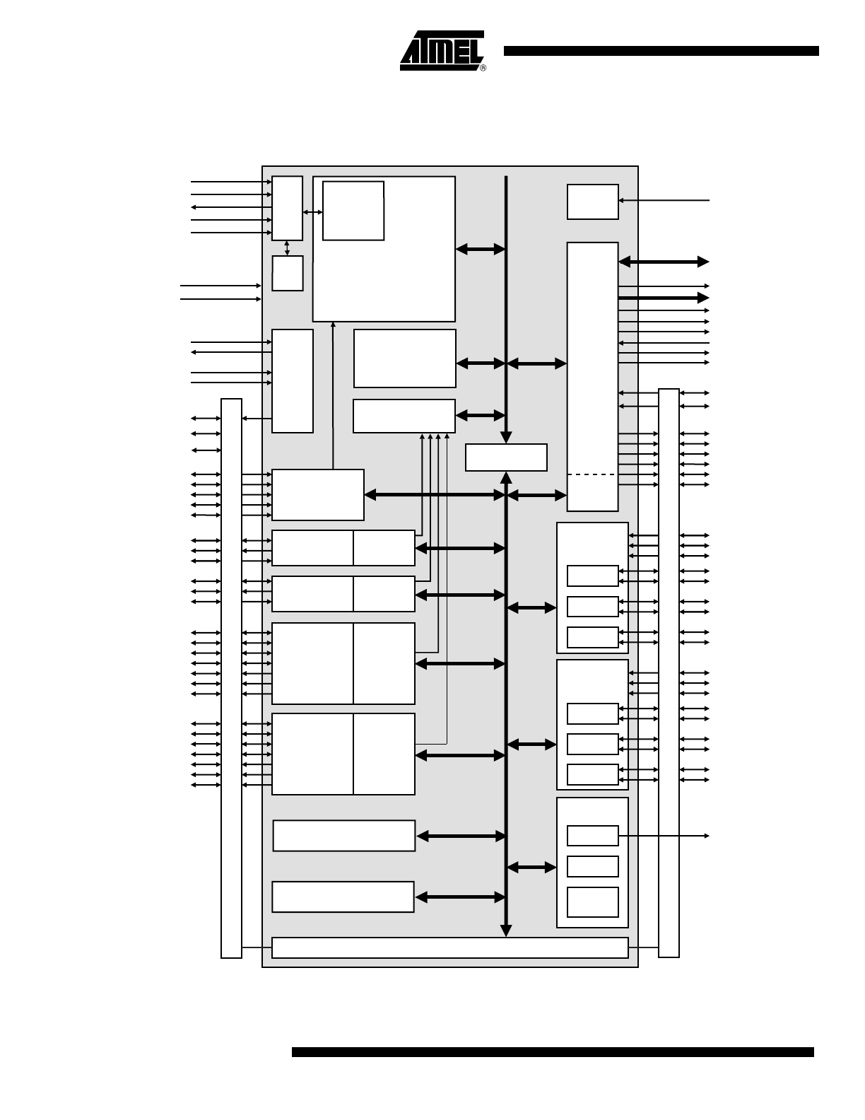
4.
Block Diagram
Figure 4-1.
AT91M42800A
ARM7TDMI
Core
Embedded
ICE
Reset
EBI: External
Bus Interface
ASB
Controller
AIC: Advanced
Interrupt Controller
AMBA™ Bridge
TC: Timer/
Counter
Block 0
TC0
TC1
TC2
USART0
USART1
2 PDC
Channels
2 PDC
Channels
APB
ASB
P
I
O
P
I
O
NRST
D0-D15
A1-A19
A0/NLB
NCS0
NCS1
PB6/TCLK0
PB9/TCLK1
PB12/TCLK2
PB7/TIOA0
PB8/TIOB0
PB10/TIOA1
PB11/TIOB1
PB13/TIOA2
PB14/TIOB2
XIN
PA25/MCKO
PA1/IRQ1
PA2/IRQ2
PA3/IRQ3
PA4/FIQ
PA5/SCK0
PA6/TXD0
PA7/RXD0
PA8/SCK1
PA9/TXD1/NTRI
PA10/RXD1
TMS
TDO
TDI
TCK
NTRST
SPIA: Serial
Peripheral
Interface
NWDOVF
TC: Timer/
Counter
Block 1
TC3
TC4
TC5
PB15/TCLK3
PB18/TCLK4
PB21/TCLK5
PB16/TIOA3
PB17/TIOB3
PB19/TIOA4
PB20/TIOB4
PB22/TIOA5
PB23/TIOB5
PA29/PME
PB1/NCS3
PA0/IRQ0
PA12/MISOA
PA13/MOSIA
PA14/NPCSA0/NSSA
PA15/NPCSA1
PA11/SPCKA
PA16/NPCSA2
PA17/NPCSA3
NRD/NOE
NWR0/NWE
NWR1/NUB
NWAIT
PB0/NCS2
Chip ID
EBI User
Interface
JT
A
G
SEL
JT
A
G
Internal RAM
8K Bytes
Cloc
k
Gener
ator
PLLRCA
PLLRCB
XOUT
PB3/A21/CS6
PB2/A20/CS7
PB5/A23/CS4
PB4/A22/CS5
System
Timers
Watchdog
Real-time
Period
Interval
PIO: Parallel I/O Controller
2 PDC
Channels
SPIB: Serial
Peripheral
Interface
PA19/MISOB
PA20/MOSIB
PA21/NPCSB0/NSSB
PA22/NPCSB1
PA18/SPCKB
PA23/NPCSB2
PA24/NPCSB3
2 PDC
Channels
PMC: Power Management
Controller
PA26
PA27/BMS
MODE0
MODE1
PA28

9
1779ES–ATARM–14-Apr-06
AT91M42800A
5.
Architectural Overview
The AT91M42800A microcontroller integrates an ARM7TDMI with its embedded ICE interface,
memories and peripherals. Its architecture consists of two main buses, the Advanced System
Bus (ASB) and the Advanced Peripheral Bus (APB). Designed for maximum performance and
controlled by the memory controller, the ASB interfaces the ARM7TDMI processor with the on-
chip 32-bit memories, the External Bus Interface (EBI) and the AMBA
™
Bridge. The AMBA
Bridge drives the APB, which is designed for accesses to on-chip peripherals and optimized for
low power consumption.
The AT91M42800A microcontroller implements the ICE port of the ARM7TDMI processor on
dedicated pins, offering a complete, low-cost and easy-to-use debug solution for target
debugging.
5.1
Memories
The AT91M42800A microcontroller embeds up to 8K bytes of internal SRAM. The internal mem-
ory is directly connected to the 32-bit data bus and is single-cycle accessible. This provides
maximum performance of 30 MIPS at 33 MHz by using the ARM instruction set of the processor.
The on-chip memory significantly reduces the system power consumption and improves its per-
formance over external memory solutions.
The AT91M42800A microcontroller features an External Bus Interface (EBI), which enables con-
nection of external memories and application-specific peripherals. The EBI supports 8- or 16-bit
devices and can use two 8-bit devices to emulate a single 16-bit device. The EBI implements the
early read protocol, enabling faster single clock cycle accesses two times faster than standard
memory interfaces.
5.2
Peripherals
The AT91M42800A microcontroller integrates several peripherals, which are classified as sys-
tem or user peripherals. All on-chip peripherals are 32-bit accessible by the AMBA Bridge, and
can be programmed with a minimum number of instructions. The peripheral register set is com-
posed of control, mode, data, status and enable/disable/status registers.
An on-chip Peripheral Data Controller (PDC) transfers data between the on-chip USARTs/SPIs
and the on- and off-chip memories without processor intervention. Most importantly, the PDC
removes the processor interrupt handling overhead and significantly reduces the number of
clock cycles required for a data transfer. It can transfer up to 64K continuous bytes without
reprogramming the start address. As a result, the performance of the microcontroller is
increased and the power consumption reduced.
5.2.1
System Peripherals
The External Bus Interface (EBI) controls the external memory and peripheral devices via an 8-
or 16-bit data bus and is programmed through the APB. Each chip select line has its own pro-
gramming register.
The Power Management Controller (PMC) optimizes power consumption of the product by con-
trolling the clocking elements such as the oscillator and the two PLLs, system and user
peripheral clocks.
The Advanced Interrupt Controller (AIC) controls the internal sources from the internal peripher-
als and the five external interrupt lines (including the FIQ) to provide an interrupt and/or fast

10
1779ES–ATARM–14-Apr-06
AT91M42800A
interrupt request to the ARM7TDMI. It integrates an 8-level priority controller, and, using the
Auto-vectoring feature, reduces the interrupt latency time.
The Parallel Input/Output Controllers (PIOA, PIOB) controls up to 54 I/O lines. It enables the
user to select specific pins for on-chip peripheral input/output functions, and general-purpose
input/output signal pins. The PIO controllers can be programmed to detect an interrupt on a sig-
nal change from each line.
There are three embedded system timers. The Real-time Timer (RTT) counts elapsed seconds
and can generate periodic or programmed interrupts. The Period Interval Timer (PIT) can be
used as a user-programmable time-base, and can generate periodic ticks. The Watchdog (WD)
can be used to prevent system lock-up if the software becomes trapped in a deadlock.
The Special Function (SF) module integrates the Chip ID and the Reset Status registers.
5.2.2
User Peripherals
Two USARTs, independently configurable, enable communication at a high baud rate in syn-
chronous or asynchronous mode. The format includes start, stop and parity bits and up to 9 data
bits. Each USART also features a Time-out and a Time-guard register, facilitating the use of the
two dedicated Peripheral Data Controller (PDC) channels.
The two 3-channel, 16-bit Timer/Counters (TC) are highly-programmable and support capture or
waveform modes. Each TC channel can be programmed to measure or generate different kinds
of waves, and can detect and control two input/output signals. Each TC also has three external
clock signals.
Two independently configurable SPIs provide communication with external devices in master or
slave mode. Each has four external chip selects which can be connected to up to 15 devices.
The data length is programmable, from 8- to 16-bit.
6.
Associated Documentation
Table 6-1.
Associated Documentation
Product
Information
Document Title
AT91M42800A
Internal architecture of processor
ARM/Thumb instruction sets
Embedded in-circuit-emulator
ARM7TDMI (Thumb) Datasheet
External memory interface mapping
Peripheral operations
Peripheral user interfaces
AT91M42800A Datasheet
DC characteristics
Power consumption
Thermal and reliability considerations
AC characteristics
AT91M42800A Electrical Characteristics
Product overview
Ordering information
Packaging information
Soldering profile
AT91M42800A Summary Datasheet (this document)
Features
•
Utilizes the ARM7TDMI
®
ARM
®
Thumb
®
Processor Core
– High-performance 32-bit RISC Architecture
– High-density 16-bit Instruction Set
– Leader in MIPS/Watt
– Embedded ICE (In-circuit Emulation)
•
8K Bytes Internal SRAM
•
Fully Programmable External Bus Interface (EBI)
– Maximum External Address Space of 64M Bytes
– Up to 8 Chip Selects
– Software Programmable 8/16-bit External Data Bus
•
8-channel Peripheral Data Controller
•
8-level Priority, Individually Maskable, Vectored Interrupt Controller
– 5 External Interrupts, Including a High-priority, Low-latency Interrupt Request
•
54 Programmable I/O Lines
•
6-channel 16-bit Timer/Counter
– 6 External Clock Inputs, 2 Multi-purpose I/O Pins per Channel
•
2 USARTs
– 2 Dedicated Peripheral Data Controller (PDC) Channels per USART
– Support for up to 9-bit Data Transfers
•
2 Master/Slave SPI Interfaces
– 2 Dedicated Peripheral Data Controller (PDC) Channels per SPI
– 8- to 16-bit Programmable Data Length
– 4 External Slave Chip Selects per SPI
•
3 System Timers:
– Period Interval Timer (PIT); Real-time Timer (RTT); Watchdog Timer (WDT)
•
Power Management Controller (PMC)
– CPU and Peripherals Can be Deactivated Individually
•
Clock Generator with 32.768 kHz Low-power Oscillator and PLL
– Support for 38.4 kHz Crystals
– Software Programmable System Clock (up to 33 MHz)
•
IEEE
®
1149.1 JTAG Boundary Scan on All Active Pins
•
Fully Static Operation: 0 Hz to 33 MHz Internal Frequency Range
at VDDCORE = 3.0V, 85
°
C
•
2.7V to 3.6V Core and PLL Operating Voltage Range; 2.7V to 5.5V I/O Operating Voltage
Range
•
-40
°
C to +85
°
C Temperature Range
•
Available in a 144-lead LQFP Package (Green) and a 144-ball BGA Package (RoHS-
compliant)
1.
Description
The AT91M42800A is a member of the Atmel AT91 16/32-bit microcontroller family,
which is based on the ARM7TDMI processor core. This processor has a high-perfor-
mance 32-bit RISC architecture with a high-density 16-bit instruction set and very low
power consumption. In addition, a large number of internally banked registers result in
very fast exception handling, making the device ideal for real-time control applica-
tions. The AT91 ARM-based MCU family also features Atmel’s high-density, in-
system programmable, nonvolatile memory technology. The AT91M42800A has a
direct connection to off-chip memory, including Flash, through the External Bus
Interface.
AT91
ARM Thumb
Microcontrollers
AT91M42800A
Summary
Rev. 1779ES–ATARM–14-Apr-06
Note: This is a summary document. A complete document is
available on our web site at www.atmel.com.
2
1779ES–ATARM–14-Apr-06
AT91M42800A
The Power Management Controller allows the user to adjust device activity according to system
requirements, and, with the 32.768 kHz low-power oscillator, enables the AT91M42800A to
reduce power requirements to an absolute minimum. The AT91M42800A is manufactured using
Atmel’s high-density CMOS technology. By combining the ARM7TDMI processor core with on-
chip SRAM and a wide range of peripheral functions including timers, serial communication con-
trollers and a versatile clock generator on a monolithic chip, the AT91M42800A provides a
highly-flexible and cost-effective solution to many compute-intensive applications.
2.
Pin Configuration
Figure 2-1.
Pin Configuration in LQFP144 Package (Top View)
1
36
144
109
108
73
37
72
AT91M42800 33AI
3
1779ES–ATARM–14-Apr-06
AT91M42800A
Figure 2-2.
Pin Configuration in BGA144 Package (Top View)
1
2
3
4
5
6
7
8
9
10
11
12
A
B
C
D
E
F
G
H
J
K
L
M
4
1779ES–ATARM–14-Apr-06
AT91M42800A
Table 2-1.
AT91M42800A Pinout in LQFP 144 Package
Pin#
Name
Pin#
Name
Pin#
Name
Pin#
Name
1
GND
37
GND
73
GND
109
GND
2
GND
38
GND
74
GND
110
GND
3
NLB/A0
39
D4
75
PB22/TIOA5
111
PA26
4
A1
40
D5
76
PB23/TIOB5
112
MODE0
5
A2
41
D6
77
PA0/IRQ0
113
XIN
6
A3
42
D7
78
PA1/IRQ1
114
XOUT
7
A4
43
D8
79
PA2/IRQ2
115
GND
8
A5
44
D9
80
PA3/IRQ3
116
PLLRCA
9
A6
45
D10
81
PA4/FIQ
117
VDDPLL
10
A7
46
D11
82
PA5/SCK0
118
PLLRCB
11
A8
47
D12
83
PA6/TXD0
119
VDDPLL
12
VDDIO
48
VDDIO
84
VDDIO
120
VDDIO
13
GND
49
GND
85
GND
121
GND
14
A9
50
D13
86
PA7/RXD0
122
NWDOVF
15
A10
51
D14
87
PA8/SCK1
123
PA27/BMS
16
A11
52
D15
88
PA9/TXD1/NTRI
124
MODE1
17
A12
53
PB6/TCLK0
89
PA10/RXD1
125
TMS
18
A13
54
PB7/TIOA0
90
PA11/SPCKA
126
TDI
19
A14
55
PB8/TIOB0
91
PA12/MISOA
127
TDO
20
A15
56
PB9/TCLK1
92
PA13/MOSIA
128
TCK
21
A16
57
PB10/TIOA1
93
PA14/NPCSA0/NSSA
129
NTRST
22
A17
58
PB11/TIOB1
94
PA15/NPCSA1
130
NRST
23
A18
59
PB12/TCLK2
95
PA16/NPCSA2
131
PA28
24
VDDIO
60
VDDIO
96
VDDIO
132
VDDIO
25
GND
61
GND
97
GND
133
GND
26
A19
62
PB13/TIOA2
98
PA17/NPCSA3
134
PA29/PME
27
PB2/A20/CS7
63
PB14/TIOB2
99
PA18/SPCKB
135
NWAIT
28
PB3/A21/CS6
64
PB15/TCLK3
100
PA19/MISOB
136
NOE/NRD
29
PB4/A22/CS5
65
PB16/TIOA3
101
PA20/MOSIB
137
NWE/NWR0
30
PB5/A23/CS4
66
PB17/TIOB3
102
PA21/NPCSB0/NSSB
138
NUB/NWR1
31
D0
67
PB18/TCLK4
103
PA22/NPCSB1
139
NCS0
32
D1
68
PB19/TIOA4
104
PA23/NPCSB2
140
NCS1
33
D2
69
PB20/TIOB4
105
PA24/NPCSB3
141
PB0/NCS2
34
D3
70
PB21/TCLK5
106
PA25/MCKO
142
PB1/NCS3
35
VDDCORE
71
VDDCORE
107
VDDCORE
143
VDDCORE
36
VDDIO
72
VDDIO
108
VDDIO
144
VDDIO
5
1779ES–ATARM–14-Apr-06
AT91M42800A
Table 2-2.
AT91M42800A Pinout in BGA 144 Package
Pin#
Name
Pin#
Name
Pin#
Name
Pin#
Name
A1
PB1/NCS3
D1
A2
G1
A17
K1
D1
A2
NCS0
D2
A3
G2
A16
K2
VDDCORE
A3
NCS1
D3
A4
G3
A11
K3
VDDIO
A4
GND
D4
NWAIT
G4
A13
K4
D9
A5
PLLRCB
D5
PA29/PME
G5
GND
K5
D10
A6
GND
D6
PA28
G6
GND
K6
D14
A7
PLLRCA
D7
TCK
G7
GND
K7
PB9/TCLK1
A8
GND
D8
TMS
G8
GND
K8
PB13/TIOA2
A9
XOUT
D9
MODE1
G9
PA9/TXD1/NTRI
K9
PB11/TIOB1
A10
XIN
D10
PA25/MCKO
G10
PA10/RXD1
K10
VDDIO
A11
MODE0
D11
PA21/NPCSB0
G11
PA8/SCK1
K11
PB16/TIOA3
A12
PA22/NPCSB1
D12
PA18/SPCKB
G12
PA7/RXD0
K12
PB23/TIOB5
B1
NUB/NWR1
E1
A7
H1
A18
L1
D3
B2
PB0/NCS2
E2
VDDIO
H2
VDDIO
L2
D2
B3
VDDCORE
E3
A6
H3
A15
L3
D5
B4
NWE/NWR0
E4
A5
H4
A14
L4
D8
B5
VDDPLL
E5
GND
H5
A19
L5
VDDIO
B6
TDO
E6
GND
H6
GND
L6
D13
B7
VDDPLL
E7
GND
H7
GND
L7
PB8/TIOB0
B8
NWDOVF
E8
NTRST
H8
GND
L8
VDDIO
B9
PA26
E9
PA13/MOSIA
H9
PA6/TXD0
L9
PB17/TIOB3
B10
PA19/MISOB
E10
PA16/NPCSA2
H10
PA4/FIQ
L10
VDDCORE
B11
PA24/NPCSB3
E11
VDDIO
H11
VDDIO
L11
PB20/TIOB4
B12
PA23/NPCSB2
E12
PA17/NPCSA3
H12
PA5/SCK0
L12
PB22/TIOA5
C1
NLB/A0
F1
A8
J1
PB5/A23/CS4
M1
D4
C2
A1
F2
A12
J2
D0
M2
D6
C3
VDDIO
F3
A9
J3
PB4/A22/CS5
M3
D7
C4
NOE/NRD
F4
A10
J4
PB3/A21/CS6
M4
D11
C5
VDDIO
F5
GND
J5
PB2/A20/CS7
M5
D12
C6
NRST
F6
GND
J6
D15
M6
PB7/TIOA0
C7
TDI
F7
GND
J7
PB6/TCLK0
M7
PB12/TCLK2
C8
VDDIO
F8
GND
J8
PB10/TIOA1
M8
PB15/TCLK3
C9
PA27/BMS
F9
PA12/MISOA
J9
PA3/IRQ3
M9
PB14/TIOB2
C10
VDDIO
F10
PA15/NPCSA1
J10
PA2/IRQ2
M10
PB18/TCLK4
C11
VDDCORE
F11
PA11/SPCKA
J11
PA0/IRQ0
M11
PB19/TIOA4
C12
PA20/MOSIB
F12
PA14/NPCSA0
J12
PA1/IRQ1
M12
PB21/TCLK5
6
1779ES–ATARM–14-Apr-06
AT91M42800A
3.
Pin Description
Table 3-1.
AT91M42800A Pin Description
Module
Name
Function
Type
Active
Level
Comments
EBI
A0 - A23
Address Bus
Output
–
All valid after reset
D0 - D15
Data Bus
I/O
–
CS4 - CS7
Chip Select
Output
High
A23 - A20 after reset
NCS0 - NCS3
Chip Select
Output
Low
NWR0
Lower Byte 0 Write Signal
Output
Low
Used in Byte Write option
NWR1
Lower Byte 1 Write Signal
Output
Low
Used in Byte Write option
NRD
Read Signal
Output
Low
Used in Byte Write option
NWE
Write Enable
Output
Low
Used in Byte Select option
NOE
Output Enable
Output
Low
Used in Byte Select option
NUB
Upper Byte Select (16-bit SRAM)
Output
Low
Used in Byte Select option
NLB
Lower Byte Select (16-bit SRAM)
Output
Low
Used in Byte Select option
NWAIT
Wait Input
Input
Low
BMS
Boot Mode Select
Input
–
Sampled during reset
PME
Protect Mode Enable
Input
High
PIO-controlled after reset
AIC
IRQ0 - IRQ3
External Interrupt Request
Input
–
PIO-controlled after reset
FIQ
Fast External Interrupt Request
Input
–
PIO-controlled after reset
TC
TCLK0 - TCLK5
Timer External Clock
Input
–
PIO-controlled after reset
TIOA0 - TIOA5
Multi-purpose Timer I/O Pin A
I/O
–
PIO-controlled after reset
TIOB0 - TIOB5
Multi-purpose Timer I/O Pin B
I/O
–
PIO-controlled after reset
USART
SCK0 - SCK1
External Serial Clock I/O
–
PIO-controlled
after
reset
TXD0 - TXD1
Transmit Data Output
Output
–
PIO-controlled after reset
RXD0 - RXD1
Receive Data Input
Input
–
PIO-controlled after reset
SPIA
SPIB
SPCKA/SPCKB
Clock
I/O
–
PIO-controlled after reset
MISOA/MISOB
Master In Slave Out
I/O
–
PIO-controlled after reset
MOSIA/MOSIB
Master Out Slave In
I/O
–
PIO-controlled after reset
NSSA/NSSB
Slave Select
Input
Low
PIO-controlled after reset
NPCSA0 - NPCSA3
NPCSB0 - NPCSB3
Peripheral Chip Selects
Output
Low
PIO-controlled after reset
PIO
PA0 - PA29
Programmable I/O Port A
I/O
–
Input after reset
PB0 - PB23
Programmable I/O Port B
I/O
–
Input after reset
ST
NWDOVF
Watchdog Timer Overflow
Output
Low
Open drain
7
1779ES–ATARM–14-Apr-06
AT91M42800A
CLOCK
XIN
Oscillator Input or External Clock
Input
–
XOUT
Oscillator Output
Output
–
PLLRCA
RC Filter for PLL A
Input
–
PLLRCB
RC Filter for PLL B
Input
–
MCKO
Clock Output
Output
–
Test and
Reset
NRST
Hardware Reset Input
Input
Low
Schmitt trigger
MODE0 - MODE1
Mode Selection
Input
–
JTAG/ICE
TMS
Test Mode Select
Input
–
Schmitt trigger, internal pull-up
TDI
Test Data In
Input
–
Schmitt trigger, internal pull-up
TDO
Test Data Out
Output
–
TCK
Test Clock
Input
–
Schmitt trigger, internal pull-up
NTRST
Test Reset Input
Input
Low
Schmitt trigger, internal pull-up
Emulation
NTRI
Tri-state Mode Enable
Input
Low
Sampled during reset
Power
VDDIO
I/O Power
Power
–
3V or 5V nominal supply
VDDCORE
Core Power
Power
–
3V nominal supply
VDDPLL
PLL Power
Power
–
3V nominal supply
GND
Ground
Ground
–
Table 3-1.
AT91M42800A Pin Description (Continued)
Module
Name
Function
Type
Active
Level
Comments
8
1779ES–ATARM–14-Apr-06
AT91M42800A
4.
Block Diagram
Figure 4-1.
AT91M42800A
ARM7TDMI
Core
Embedded
ICE
Reset
EBI: External
Bus Interface
ASB
Controller
AIC: Advanced
Interrupt Controller
AMBA™ Bridge
TC: Timer/
Counter
Block 0
TC0
TC1
TC2
USART0
USART1
2 PDC
Channels
2 PDC
Channels
APB
ASB
P
I
O
P
I
O
NRST
D0-D15
A1-A19
A0/NLB
NCS0
NCS1
PB6/TCLK0
PB9/TCLK1
PB12/TCLK2
PB7/TIOA0
PB8/TIOB0
PB10/TIOA1
PB11/TIOB1
PB13/TIOA2
PB14/TIOB2
XIN
PA25/MCKO
PA1/IRQ1
PA2/IRQ2
PA3/IRQ3
PA4/FIQ
PA5/SCK0
PA6/TXD0
PA7/RXD0
PA8/SCK1
PA9/TXD1/NTRI
PA10/RXD1
TMS
TDO
TDI
TCK
NTRST
SPIA: Serial
Peripheral
Interface
NWDOVF
TC: Timer/
Counter
Block 1
TC3
TC4
TC5
PB15/TCLK3
PB18/TCLK4
PB21/TCLK5
PB16/TIOA3
PB17/TIOB3
PB19/TIOA4
PB20/TIOB4
PB22/TIOA5
PB23/TIOB5
PA29/PME
PB1/NCS3
PA0/IRQ0
PA12/MISOA
PA13/MOSIA
PA14/NPCSA0/NSSA
PA15/NPCSA1
PA11/SPCKA
PA16/NPCSA2
PA17/NPCSA3
NRD/NOE
NWR0/NWE
NWR1/NUB
NWAIT
PB0/NCS2
Chip ID
EBI User
Interface
JT
A
G
SEL
JT
A
G
Internal RAM
8K Bytes
Cloc
k
Gener
ator
PLLRCA
PLLRCB
XOUT
PB3/A21/CS6
PB2/A20/CS7
PB5/A23/CS4
PB4/A22/CS5
System
Timers
Watchdog
Real-time
Period
Interval
PIO: Parallel I/O Controller
2 PDC
Channels
SPIB: Serial
Peripheral
Interface
PA19/MISOB
PA20/MOSIB
PA21/NPCSB0/NSSB
PA22/NPCSB1
PA18/SPCKB
PA23/NPCSB2
PA24/NPCSB3
2 PDC
Channels
PMC: Power Management
Controller
PA26
PA27/BMS
MODE0
MODE1
PA28
9
1779ES–ATARM–14-Apr-06
AT91M42800A
5.
Architectural Overview
The AT91M42800A microcontroller integrates an ARM7TDMI with its embedded ICE interface,
memories and peripherals. Its architecture consists of two main buses, the Advanced System
Bus (ASB) and the Advanced Peripheral Bus (APB). Designed for maximum performance and
controlled by the memory controller, the ASB interfaces the ARM7TDMI processor with the on-
chip 32-bit memories, the External Bus Interface (EBI) and the AMBA
™
Bridge. The AMBA
Bridge drives the APB, which is designed for accesses to on-chip peripherals and optimized for
low power consumption.
The AT91M42800A microcontroller implements the ICE port of the ARM7TDMI processor on
dedicated pins, offering a complete, low-cost and easy-to-use debug solution for target
debugging.
5.1
Memories
The AT91M42800A microcontroller embeds up to 8K bytes of internal SRAM. The internal mem-
ory is directly connected to the 32-bit data bus and is single-cycle accessible. This provides
maximum performance of 30 MIPS at 33 MHz by using the ARM instruction set of the processor.
The on-chip memory significantly reduces the system power consumption and improves its per-
formance over external memory solutions.
The AT91M42800A microcontroller features an External Bus Interface (EBI), which enables con-
nection of external memories and application-specific peripherals. The EBI supports 8- or 16-bit
devices and can use two 8-bit devices to emulate a single 16-bit device. The EBI implements the
early read protocol, enabling faster single clock cycle accesses two times faster than standard
memory interfaces.
5.2
Peripherals
The AT91M42800A microcontroller integrates several peripherals, which are classified as sys-
tem or user peripherals. All on-chip peripherals are 32-bit accessible by the AMBA Bridge, and
can be programmed with a minimum number of instructions. The peripheral register set is com-
posed of control, mode, data, status and enable/disable/status registers.
An on-chip Peripheral Data Controller (PDC) transfers data between the on-chip USARTs/SPIs
and the on- and off-chip memories without processor intervention. Most importantly, the PDC
removes the processor interrupt handling overhead and significantly reduces the number of
clock cycles required for a data transfer. It can transfer up to 64K continuous bytes without
reprogramming the start address. As a result, the performance of the microcontroller is
increased and the power consumption reduced.
5.2.1
System Peripherals
The External Bus Interface (EBI) controls the external memory and peripheral devices via an 8-
or 16-bit data bus and is programmed through the APB. Each chip select line has its own pro-
gramming register.
The Power Management Controller (PMC) optimizes power consumption of the product by con-
trolling the clocking elements such as the oscillator and the two PLLs, system and user
peripheral clocks.
The Advanced Interrupt Controller (AIC) controls the internal sources from the internal peripher-
als and the five external interrupt lines (including the FIQ) to provide an interrupt and/or fast
10
1779ES–ATARM–14-Apr-06
AT91M42800A
interrupt request to the ARM7TDMI. It integrates an 8-level priority controller, and, using the
Auto-vectoring feature, reduces the interrupt latency time.
The Parallel Input/Output Controllers (PIOA, PIOB) controls up to 54 I/O lines. It enables the
user to select specific pins for on-chip peripheral input/output functions, and general-purpose
input/output signal pins. The PIO controllers can be programmed to detect an interrupt on a sig-
nal change from each line.
There are three embedded system timers. The Real-time Timer (RTT) counts elapsed seconds
and can generate periodic or programmed interrupts. The Period Interval Timer (PIT) can be
used as a user-programmable time-base, and can generate periodic ticks. The Watchdog (WD)
can be used to prevent system lock-up if the software becomes trapped in a deadlock.
The Special Function (SF) module integrates the Chip ID and the Reset Status registers.
5.2.2
User Peripherals
Two USARTs, independently configurable, enable communication at a high baud rate in syn-
chronous or asynchronous mode. The format includes start, stop and parity bits and up to 9 data
bits. Each USART also features a Time-out and a Time-guard register, facilitating the use of the
two dedicated Peripheral Data Controller (PDC) channels.
The two 3-channel, 16-bit Timer/Counters (TC) are highly-programmable and support capture or
waveform modes. Each TC channel can be programmed to measure or generate different kinds
of waves, and can detect and control two input/output signals. Each TC also has three external
clock signals.
Two independently configurable SPIs provide communication with external devices in master or
slave mode. Each has four external chip selects which can be connected to up to 15 devices.
The data length is programmable, from 8- to 16-bit.
6.
Associated Documentation
Table 6-1.
Associated Documentation
Product
Information
Document Title
AT91M42800A
Internal architecture of processor
ARM/Thumb instruction sets
Embedded in-circuit-emulator
ARM7TDMI (Thumb) Datasheet
External memory interface mapping
Peripheral operations
Peripheral user interfaces
AT91M42800A Datasheet
DC characteristics
Power consumption
Thermal and reliability considerations
AC characteristics
AT91M42800A Electrical Characteristics
Product overview
Ordering information
Packaging information
Soldering profile
AT91M42800A Summary Datasheet (this document)