
2017 Microchip Technology Inc.
DS20005808A-page 1
DSC63XX
Features
• Output Frequency: 1 MHz to 100 MHz LVCMOS
• Spread Spectrum Options:
- Center Spread: ±0.25%, ±0.5%, ±1.0%,
±1.5%, ±2.0%, ±2.5%
- Down Spread: –0.5%, –1.0%, –1.5%, –2.0%,
–2.5%, –3.0%
• Ultra-Low Power Consumption: 3 mA (Active),
12
A (Standby)
• Wide Supply Voltage Range: 1.71V ~ 3.63V V
DD
• Ultra-Small Package Sizes:
- 1.6 mm
1.2 mm
- 2.0 mm
1.6 mm
- 2.5 mm
2.0 mm
- 3.2 mm
2.5 mm
• Industrial Temperature Range: –40°C to 85°C
• Excellent Shock and Vibration Immunity
• High Reliability
• Lead Free and RoHS Compliant
Applications
• Flat Panel Display/Monitor
• Multi-Function Printer
• Digital Signage
• Consumer Electronics
General Description
The DSC63xx family of devices is the industry’s
smallest and lowest-power spread-spectrum MEMS
oscillators. Available in four different package sizes
with operation as low as 3 mA, the smallest 4-pin
package is a mere 1.6 mm x 1.2 mm in size. The
devices support up to ±2.5% or –3% spread spectrum
that can achieve up to 15 dB electromagnetic
interference (EMI) reduction. Because of industry
standard package and pin options, customers can
solve last minute EMI problems simply by putting the
new DSC63xx on their current board layout with no
redesign required.
The DSC63xx family is available in ultra-small 1.6 mm
x 1.2 mm and 2.0 mm x 1.6 mm packages. Other
package sizes include: 2.5 mm x 2.0 mm and 3.2 mm x
2.5 mm. These packages are “drop-in” replacements
for standard 4-pin CMOS quartz crystal oscillators.
Ultra-Small, Ultra-Low Power MEMS Oscillator with Spread Spectrum
DSC63XX
DS20005808A-page 2
2017 Microchip Technology Inc.
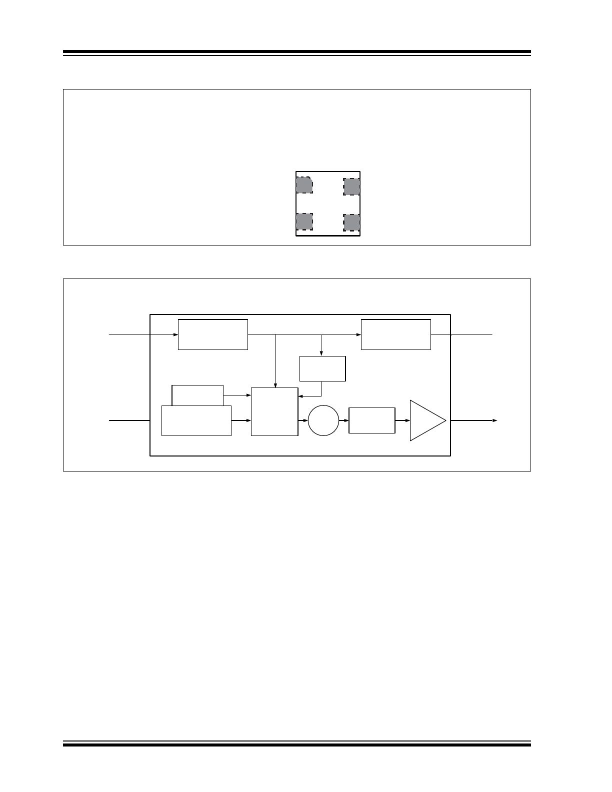
Package Types
Block Diagram
DSC63
XX
3.2 mm x 2.5 mm DFN
2.5 mm x 2.0 mm LGA
2.0 mm x 1.6 mm LGA
1.6 mm x 1.2 mm LGA
(Top View)
OE/STDBY/SSEN
4
GND
VDD
OUT
3
2
1
DSC63
XX
MEMS
RESONATOR
TEMP SENSOR
CONTROL &
COMPENSATION
PLL
VCO
OUTPUT
DIVIDER
DRIVER
SUPPLY
REGULATION
PIN 1
OE/STBY/SSEN
PIN 2
GND
PIN 4
VDD
PIN 3
OUTPUT
DIGITAL
CONTROL
SST
2017 Microchip Technology Inc.
DS20005808A-page 3
DSC63XX
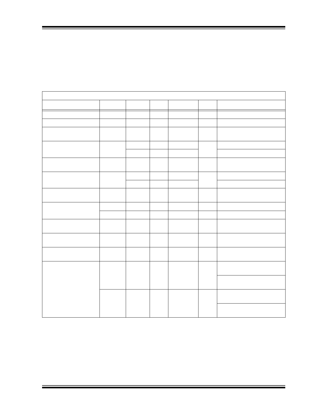
1.0
ELECTRICAL CHARACTERISTICS
Absolute Maximum Ratings
Supply Voltage .......................................................................................................................................... –0.3V to +4.0V
Input Voltage (V
IN
) ..............................................................................................................................–0.3V to V
DD
+0.3V
ESD Protection ............................................................................................................ 4 kV HBM, 400V MM, 2 kV CDM
DSC63XX ELECTRICAL CHARACTERISTICS
Electrical Characteristics: Unless otherwise indicated, V
DD
= 1.8V –5% to 3.3V +10%, T
A
= –40°C to 85°C.
Parameters
Sym.
Min.
Typ.
Max.
Units
Conditions
Supply Voltage,
Note 1
V
DD
1.71
—
3.63
V
—
Power Supply Ramp
t
PU
0.1
—
100
ms
Note 8
Active Supply Current
I
DD
—
3.0
—
mA
F
OUT
= 27 MHz, V
DD
= 1.8V,
No Load
Standby Supply Current
Note 2
I
STBY
—
12
—
µA
V
DD
= 1.8/2.5V
—
80
—
V
DD
= 3.3V
Frequency Stability
Note 3
∆f
—
—
±25
±50
ppm
All temp ranges
Aging
∆f
—
—
±5
ppm
1st year @25°C
—
—
±1
Per year after first year
Startup Time
t
SU
—
—
1.3
ms
From 90% V
DD
to valid clock
output, T = 25°C
Input Logic Levels
Note 4
V
IH
0.7 x V
DD
—
—
V
Input Logic High
V
IL
—
—
0.3 x V
DD
V
Input Logic Low
Output Disable Time
Note 5
t
DA
—
—
200+Period
ns
—
Output Enable Time
Note 6
t
EN
—
—
1
µs
—
OE/STDBY/SSEN Pull-up
Resistor
Note 7
—
—
300
—
kΩ
If configured
Output Logic Levels
V
OH
0.8 x V
DD
—
—
V
Output Logic High, I = 3 mA,
Std. Drive
Output Logic High, I = 6 mA,
High Drive
V
OL
—
—
0.2 x V
DD
V
Output Logic Low, I = –3 mA,
Std. Drive
Output Logic Low, I = –6 mA,
High Drive
Note 1: Pin 4 V
DD
should be filtered with 0.1 µf capacitor.
2: Not including current through pull-up resistor on EN pin (if configured). Higher standby current seen at
>3.3V V
DD
.
3: Includes frequency variations due to initial tolerance, temperature, and power supply voltage.
4: Input waveform must be monotonic with rise/fall time < 10 ms
5: Output Disable time takes up to one period of the output waveform + 200 ns.
6: For parts configured with OE, not Standby.
7: Output is enabled if pad is floated or not connected.
8: Time to reach 90% of target V
DD
. Power ramp rise must be monotonic.
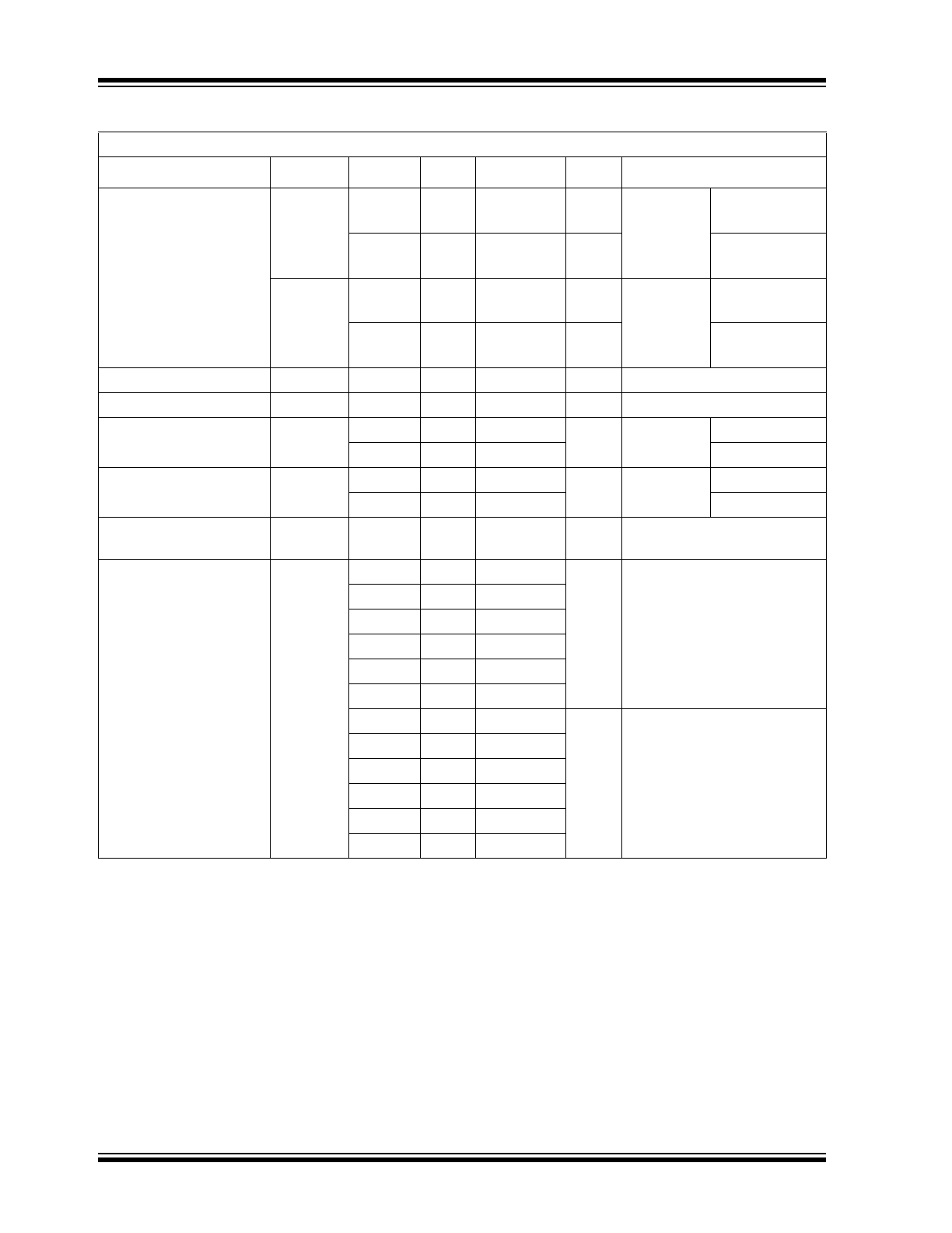
DSC63XX
DS20005808A-page 4
2017 Microchip Technology Inc.
Output Transition Time
Rise Time/Fall Time
t
RX
/t
FX
—
1
1.5
ns
DSC63x2
High Drive,
20% to 80%
C
L
= 15 pF
V
DD
= 1.8V
—
0.5
1.0
ns
V
DD
= 2.5V/3.3V
t
RY
/t
FY
—
1.2
2.0
ns
DSC63x1
Std Drive,
20% to 80%
C
L
= 10 pF
V
DD
= 1.8V
—
1
1.6
ns
V
DD
= 2.5V/3.3V
Frequency
f
0
1
—
100
MHz
—
Output Duty Cycle
SYM
45
—
55
%
—
Period Jitter, RMS
J
PER
—
14
—
ps
RMS
F
OUT
=
27 MHz
V
DD
= 1.8V
—
11
—
V
DD
= 2.5V/3.3V
Cycle-to-Cycle Jitter
(peak)
J
Cy–Cy
—
75
—
ps
F
OUT
=
27 MHz
V
DD
= 1.8V
—
53
—
V
DD
= 2.5V/3.3V
Spread Spectrum
Modulation Frequency
f
SS
—
33
—
kHz
—
Spread Spectrum
Modulation and Type
—
—
±0.25
—
%
Center Spread
—
±0.5
—
—
±1
—
—
±1.5
—
—
±2
—
—
±2.5
—
—
–0.25
—
%
Down Spread
—
–0.5
—
—
–1
—
—
–1.5
—
—
–2
—
—
–3
—
DSC63XX ELECTRICAL CHARACTERISTICS (CONTINUED)
Electrical Characteristics: Unless otherwise indicated, V
DD
= 1.8V –5% to 3.3V +10%, T
A
= –40°C to 85°C.
Parameters
Sym.
Min.
Typ.
Max.
Units
Conditions
Note 1: Pin 4 V
DD
should be filtered with 0.1 µf capacitor.
2: Not including current through pull-up resistor on EN pin (if configured). Higher standby current seen at
>3.3V V
DD
.
3: Includes frequency variations due to initial tolerance, temperature, and power supply voltage.
4: Input waveform must be monotonic with rise/fall time < 10 ms
5: Output Disable time takes up to one period of the output waveform + 200 ns.
6: For parts configured with OE, not Standby.
7: Output is enabled if pad is floated or not connected.
8: Time to reach 90% of target V
DD
. Power ramp rise must be monotonic.
2017 Microchip Technology Inc.
DS20005808A-page 5
DSC63XX
TEMPERATURE SPECIFICATIONS (
Note 1
)
Parameters
Sym.
Min.
Typ.
Max.
Units
Conditions
Temperature Ranges
Junction Operating Temperature
T
J
—
—
+150
°C
—
Ambient Operating Temperature
T
A
–40
—
+85
°C
Industrial
Ambient Operating Temperature
T
A
–20
—
+70
°C
Extended Commercial
Storage Ambient Temperature Range
T
A
–55
—
+150
°C
—
Soldering Temperature
T
S
—
+260
—
°C
40 sec. max.
Note 1: The maximum allowable power dissipation is a function of ambient temperature, the maximum allowable
junction temperature and the thermal resistance from junction to air (i.e., T
A
, T
J
, θ
JA
). Exceeding the max-
imum allowable power dissipation will cause the device operating junction temperature to exceed the max-
imum +150°C rating. Sustained junction temperatures above +150°C can impact the device reliability.
DSC63XX
DS20005808A-page 6
2017 Microchip Technology Inc.
2.0
PIN DESCRIPTIONS
The descriptions of the pins are listed in
Table 2-1
.
2.1
Output Buffer Options
The DSC63xx family is available in multiple output driver configurations.
The standard-drive (63x1) and high-drive (63x2) deliver respective output currents of greater than 3 mA and 6 mA at
20%/80% of the supply voltage. For heavy loads of 15 pF or higher, the high-drive option is recommended.
TABLE 2-1:
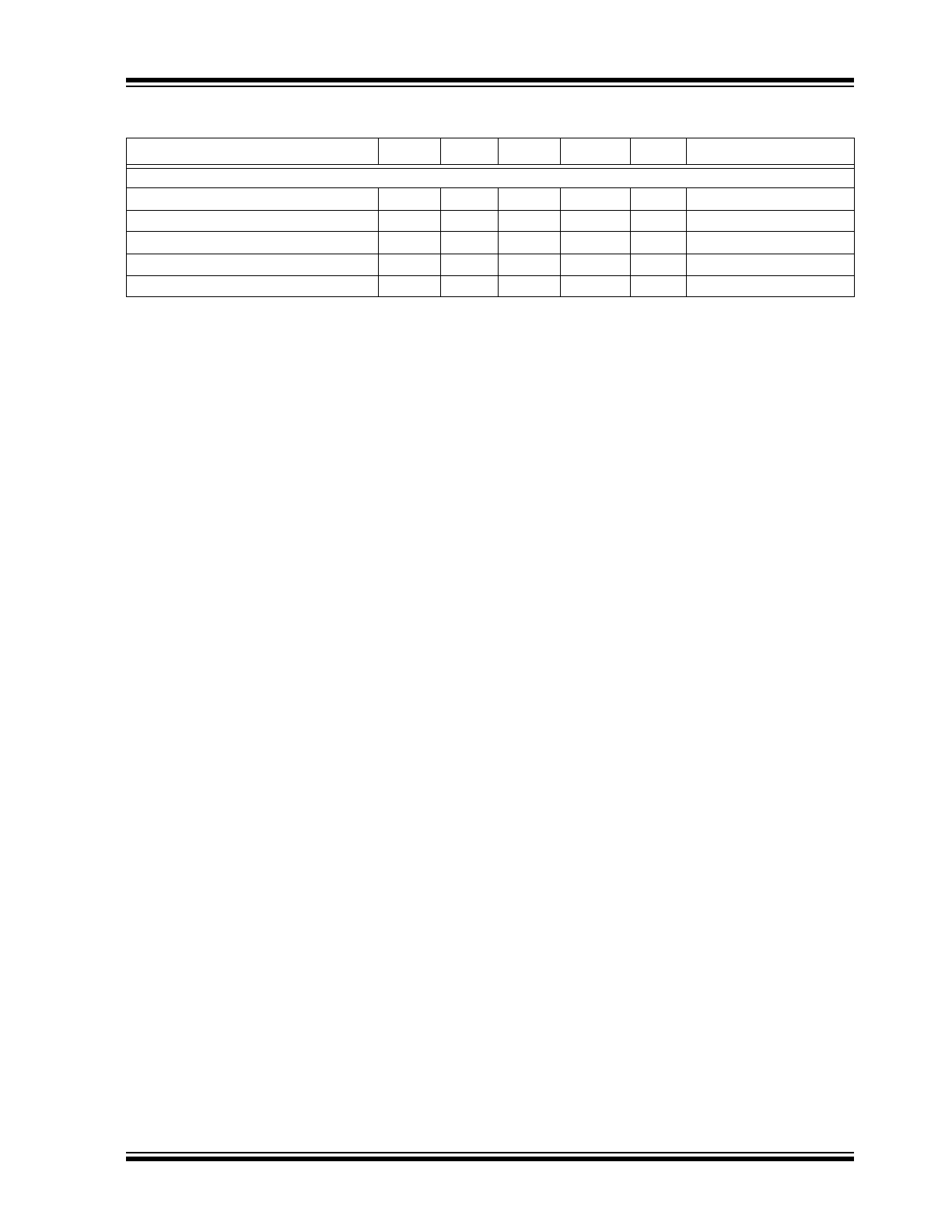
DSC63XX PIN FUNCTION TABLE (OUTPUT FREQUENCY ≥1 MHZ)
Pin Number
Pin Name
Pin Type
Description
1
OE
I
Output Enable: H = Specified Frequency Output,
Note 1
,
Note 2
L = Output is high impedance
STDBY
Standby: H = Specified Frequency Output,
Note 1
,
Note 2
L = Output is high impedance. Device is in low power
mode, supply current is at I
STBY
SSEN
Spread Spectrum Enable: H = Enabled
L = Disabled,
Note 1
2
GND
Power
Power supply ground
3
Output
O
Oscillator clock output
4
VDD
Power
Power supply,
Note 3
Note 1: DSC630x/1x/3x has 300 kΩ internal pull-up resistor on pin 1. DSC634x/5x/7x has no internal pull-up resis-
tor on pin 1 and needs an external pull-up or to be driven by other chip.
2: If pin 1 is configured as either OE or STDBY, then the Spread Spectrum is enabled by default.
3: Bypass with 0.1 µF capacitor placed as close to V
DD
pin as possible.
2017 Microchip Technology Inc.
DS20005808A-page 7
DSC63XX
3.0
DIAGRAMS
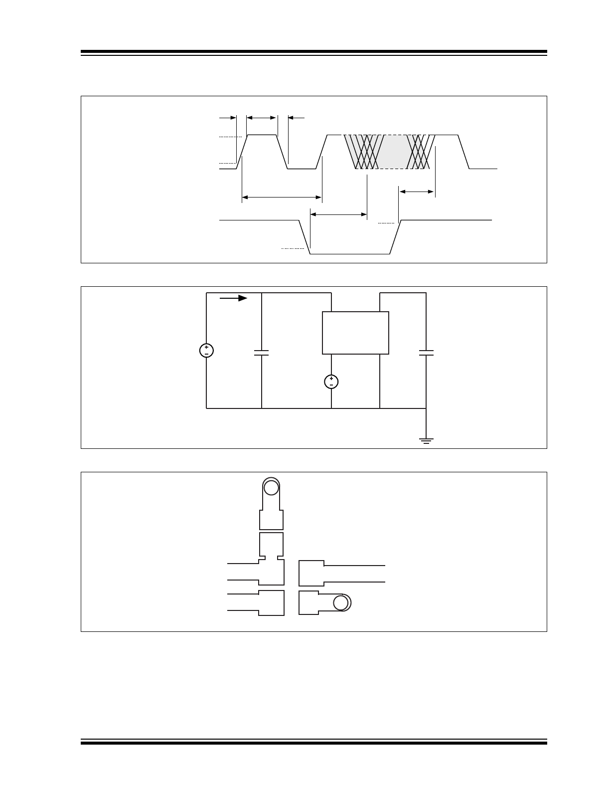
FIGURE 3-1:
Output Waveform.
FIGURE 3-2:
Test Circuit.
FIGURE 3-3:
Recommended Board Layout.
V
OH
V
OL
V
IL
1/f
o
OUTPUT
ENABLE
t
DA
t
EN
t
F
t
R
V
IH
V
DD
0.1μF
4
3
1
2
V
DA
I
DD
C
L
VDD
C1
GND
Enable
Output
Via to GND Layer
Via to GND Layer
DSC63XX
DS20005808A-page 8
2017 Microchip Technology Inc.
4.0
SPREAD SPECTRUM
Spread spectrum is a slow modulation of the clock
frequency over time. The PLL inside the MEMS
oscillator is modulated with a triangular wave at
33 kHz. With such a slow modulation, the peak spectral
energy of both the fundamental and all the harmonics
is spread over a wider frequency range and such an
energy is significantly reduced, thus providing an EMI
reduction. The triangular wave is chosen because of its
flat spectral density.
The DSC63xx MEMS oscillator family offers several
modulation options: the spreading is either center
spread or down spread with respect to the clock
frequency. Center spreading ranges from ±0.25% to
±2.5%, while down spreading ranges from –0.25% to –
3%.
If the clock frequency is 100 MHz and center spreading
with ±1% is chosen, the output clock will range from
99 MHz to 101 MHz. If down spreading with –2% is
chosen, the output clock will range from 98 MHz to
100 MHz.
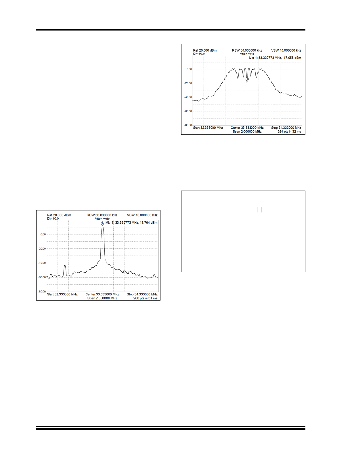
Figure 4-1
and
Figure 4-2
show a spectrum example of
the DSC6331 with a 33.333 MHz clock, modulated with
central spread of ±1%.
FIGURE 4-1:
DSC6331 Spectrum at
33.333 MHz with Modulation Turned Off.
FIGURE 4-2:
DSC6331 Spectrum at
33.333 MHz with Modulation Turned On.
It is noticeable that the spread spectrum provides a
reduction of about 10 dB from the peak power. Such a
reduction may also be estimated by the following
equation:
EQUATION 4-1:
The theoretical calculation for this example provides
10.45 dB, which is consistent with the measurement.
Similarly to the fundamental frequency, all the
harmonics are spread and attenuated in similar
fashion.
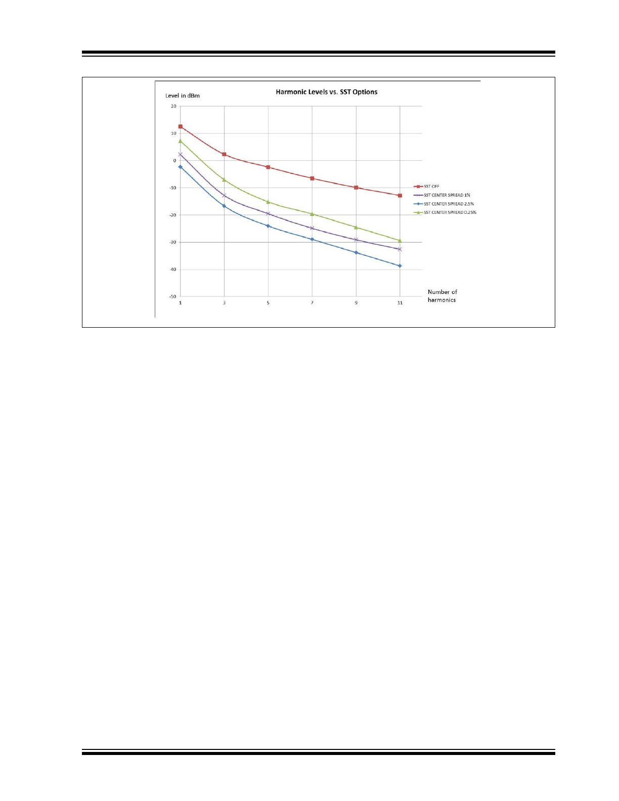
Figure 4-3
shows how the DSC6331
fundamental at 33.333 MHz and its odd harmonics are
attenuated when various types of modulations are
selected. For picture clarity, only the center spread
options are shown. However, down spread with
corresponding percentage provides the same level of
harmonic attenuation (e.g. central spread of ±1%
provides the same harmonics attenuation of down
spread with –2%).
EMI Reduction
10
Log10 S
fc
RBW
=
Where:
S
Peak-to-peak spread percentage (0.01,
this example).
fc
Carrier frequency (33.333 Mhz, this
example).
RBW
Resolution bandwidth of the spectrum
analyzer (30 kHz, this example).
2017 Microchip Technology Inc.
DS20005808A-page 9
DSC63XX
FIGURE 4-3:
DSC6331 Harmonic Levels with Various Spread Spectrum Options.
DSC63XX
DS20005808A-page 10
2017 Microchip Technology Inc.
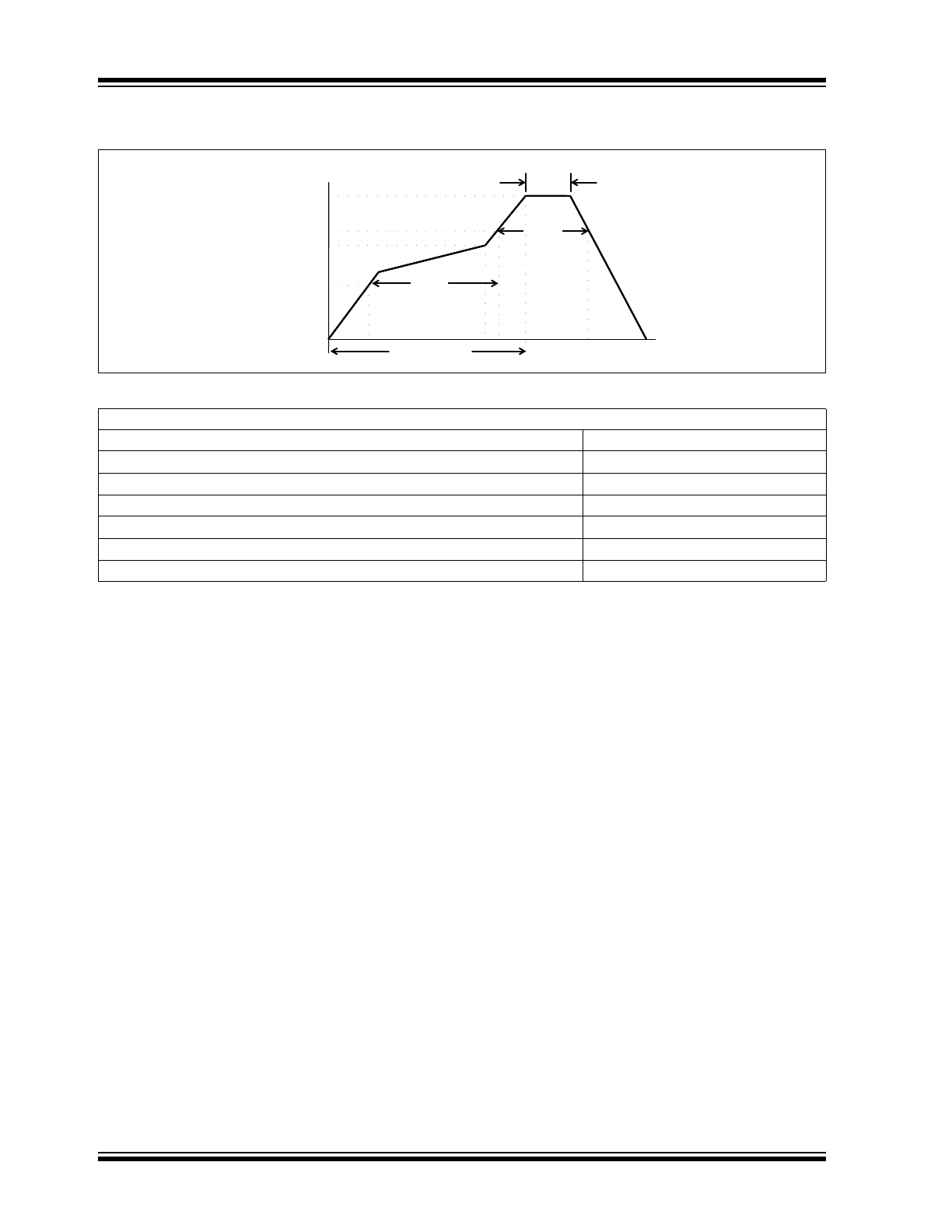
5.0
SOLDER REFLOW
FIGURE 5-1:
Solder Reflow Profile.
60-180
Seconds
Tempera
ture (°C)
260°C
3°
C/sec max.
217°C
200°C
150°C
25°C
8 minutes max.
Pre-Heat
3°
C/sec max.
Reflow
Cool
Time
6°
C/sec max.
60-150
Seconds
20-40
Seconds
MSL 1 @ 260°C refer to JSTD-020C
Ramp-Up Rate (200°C to Peak Temp)
3°C/sec max.
Pre-heat Time 150°C to 200°C
60 to 180 sec.
Time maintained above 217°C
60 to 150 sec.
Peak Temperature
255°C to 260°C
Time within 5°C of actual Peak
20 to 40 sec.
Ramp-Down Rate
6°C/sec. max.
Time 25°C to Peak Temperature
8 minutes max.