
2017 Microchip Technology Inc.
DS20005624B-page 1
DSC61XX
Features
• Wide Frequency Range: 2 kHz to 100 MHz
• Ultra-Low Power Consumption: 3 mA/12 µA
(Active/Standby)
• Ultra-Small Footprints
- 1.6 mm
1.2 mm
- 2.0 mm
1.6 mm
- 2.5 mm
2.0 mm
- 3.2 mm
2.5 mm
• Frequency Select Input Supports Two
Pre-Defined Frequencies
• High Stability: ±25 ppm, ±50 ppm
• Wide Temperature Range
- Industrial: –40°C to 85°C
- Ext. Commercial: –20° to 70°C
• Excellent Shock and Vibration Immunity
- Qualified to MIL-STD-883
• High Reliability
- 20x Better MTF Than Quartz Oscillators
• Supply Range of 1.71V to 3.63V
• Short Sample Lead Time: <2 weeks
• Lead Free & RoHS Compliant
Applications
• Low Power/Portable Applications: IoT,
Embedded/Smart Devices
• Consumer: Home Healthcare, Fitness Devices,
Home Automation
• Automotive: Rear View/Surround View Cameras,
Infotainment System
• Industrial: Building/Factory Automation,
Surveillance Camera
General Description
The DSC61xx family of MEMS oscillators combines the
industry leading low power consumption and
ultra-small packages with exceptional frequency
stability and jitter performance over temperature. The
single-output DSC61xx MEMS oscillators are excellent
choices for use as clock references in small,
battery-powered devices such as wearable and
Internet of Things (IoT) devices in which small size, low
power consumption, and long-term reliability are
paramount. They also meet the stringent mechanical
durability and reliability requirements within Automotive
Electronics Council standard Q100 (AEC-Q100), so
they are well suited for under-hood applications as well.
The DSC61xx family is available in ultra-small
1.6 mm x 1.2 mm and 2.0 mm x 1.6 mm packages.
Other package sizes include: 2.5 mm x 2.0 mm and
3.2 mm x 2.5 mm. These packages are “drop-in”
replacements for standard 4-pin CMOS quartz crystal
oscillators.
Package Types
DSC61
XX
3.2 mm x 2.5 mm DFN
2.5 mm x 2.0 mm LGA
2.0 mm x 1.6 mm LGA
1.6 mm x 1.2 mm LGA
(Top View)
OE/STBY/FS
4
GND
VDD
OUT
3
2
1
Ultra-Small, Ultra-Low Power MEMS Oscillator
DSC61XX
DS20005624B-page 2
2017 Microchip Technology Inc.
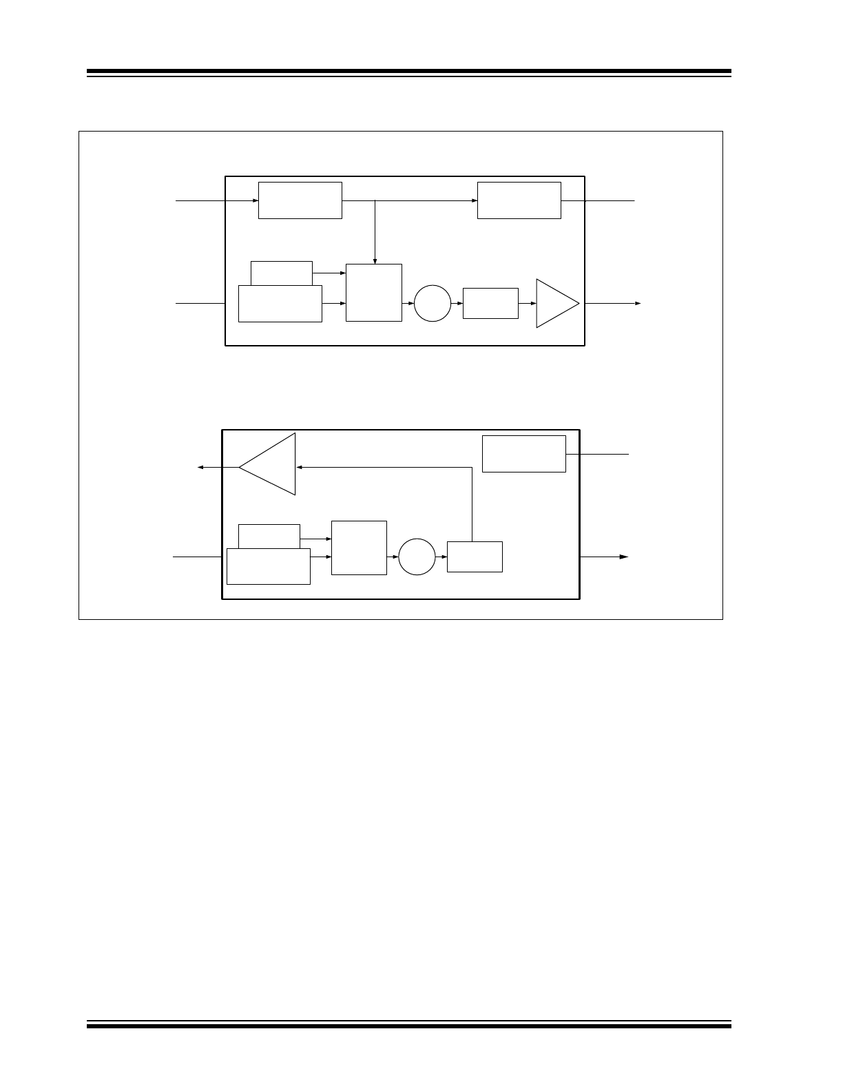
Block Diagram
DSC6101/02/11/12/21/22/41/42/51/52/61/62
DSC6183 (kHz Output)
MEMS
RESONATOR
TEMP SENSOR
CONTROL &
COMPENSATION
PLL
VCO
OUTPUT
DIVIDER
DRIVER
SUPPLY
REGULATION
PIN 1
OE/STBY/FS
PIN 2
GND
PIN 4
VDD
PIN 3
OUTPUT
DIGITAL
CONTROL
MEMS
RESONATOR
TEMP SENSOR
CONTROL &
COMPENSATION
PLL
VCO
OUTPUT
DIVIDER
SUPPLY
REGULATION
P1
OUTPUT
P2
GND
P4
VDD
P3
DNC
DRIVER
2017 Microchip Technology Inc.
DS20005624B-page 3
DSC61XX
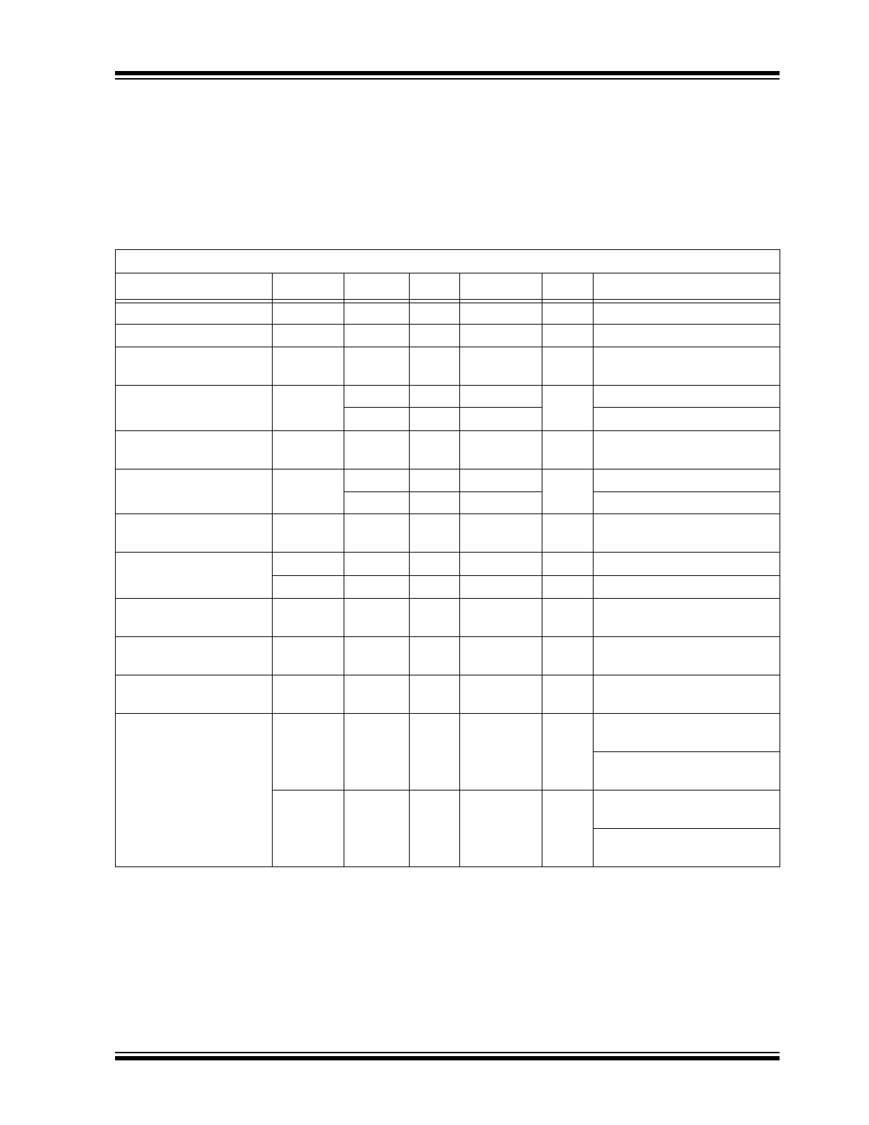
1.0
ELECTRICAL CHARACTERISTICS
Absolute Maximum Ratings
Supply Voltage .......................................................................................................................................... –0.3V to +4.0V
Input Voltage (V
IN
) ..............................................................................................................................–0.3V to V
DD
+0.3V
ESD Protection ............................................................................................................ 4 kV HBM, 400V MM, 2 kV CDM
ELECTRICAL CHARACTERISTICS
Electrical Characteristics: Unless otherwise indicated, V
DD
= 1.8V –5% to 3.3V +10%, T
A
= –40°C to 85°C.
Parameters
Sym.
Min.
Typ.
Max.
Units
Conditions
Supply Voltage,
Note 1
V
DD
1.71
—
3.63
V
—
Power Supply Ramp
t
PU
0.1
—
100
ms
Note 8
Active Supply Current
I
DD
—
3.0
—
mA
F
OUT
= 27 MHz, V
DD
= 1.8V,
No Load
Standby Supply Current
Note 2
I
STBY
—
12
—
µA
V
DD
= 1.8/2.5V
—
80
—
V
DD
= 3.3V
Frequency Stability
Note 3
∆f
—
—
±25
±50
ppm
All temp ranges
Aging
∆f
—
—
±5
ppm
1st year @ 25°C
—
—
±1
Per year after first year
Startup Time
t
SU
—
—
1.3
ms
From 90% V
DD
to valid clock
output, T = 25°C
Input Logic Levels
Note 4
V
IH
0.7 x V
DD
—
—
V
Input Logic High
V
IL
—
—
0.3 x V
DD
V
Input Logic Low
Output Disable Time
Note 5
t
DA
—
—
200+Period
ns
—
Output Enable Time
Note 6
t
EN
—
—
1
µs
—
Enable Pull-up Resistor
Note 7
—
—
300
—
kΩ
If configured
Output Logic Levels
V
OH
0.8 x V
DD
—
—
V
Output Logic High, I = 3 mA,
Std. Drive
Output Logic High, I = 6 mA,
High Drive
V
OL
—
—
0.2 x V
DD
V
Output Logic Low, I = –3 mA,
Std. Drive
Output Logic Low, I = –3 mA,
High Drive
Note 1: Pin 4 V
DD
should be filtered with 0.1 µF capacitor.
2: Not including current through pull-up resistor on EN pin (if configured). Higher standby current seen at
>3.3V V
DD
.
3: Includes frequency variations due to initial tolerance, temp. and power supply voltage.
4: Input waveform must be monotonic with rise/fall time < 10 ms
5: Output Disable time takes up to one period of the output waveform + 200 ns.
6: For parts configured with OE, not Standby.
7: Output is enabled if pad is floated or not connected.
8: Time to reach 90% of target V
DD
. Power ramp rise must be monotonic.
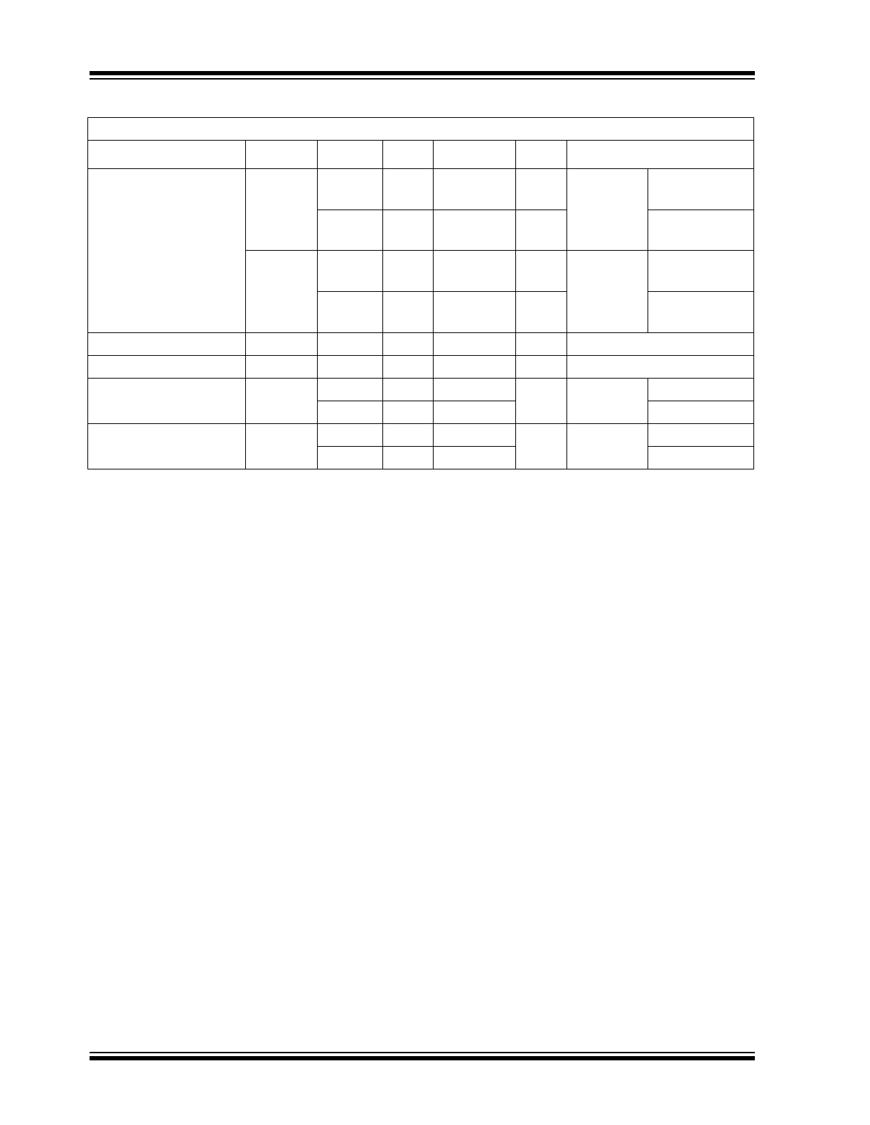
DSC61XX
DS20005624B-page 4
2017 Microchip Technology Inc.
Output Transition Time
Rise Time/Fall Time
t
RX
/t
FX
—
1
1.5
ns
DSC61x2
High Drive,
20% to 80%
C
L
= 15 pF
V
DD
= 1.8V
—
0.5
1.0
ns
V
DD
= 2.5V/3.3V
t
RY
/t
FY
—
1.2
2.0
ns
DSC61x1
Std Drive,
20% to 80%
C
L
= 10 pF
V
DD
= 1.8V
—
1.5
2.2
ns
V
DD
= 2.5V/3.3V
Frequency
f
0
0.002
—
100
MHz
Output on Pin 1 for < 1 MHz
Output Duty Cycle
SYM
45
—
55
%
—
Period Jitter, RMS
J
PER
—
9.5
11
ps
RMS
F
OUT
=
27 MHz
V
DD
= 1.8V
—
7.5
9
V
DD
= 2.5V/3.3V
Cycle-to-Cycle Jitter
(peak)
J
Cy–Cy
—
50
70
ps
F
OUT
=
27 MHz
V
DD
= 1.8V
—
35
60
V
DD
= 2.5V/3.3V
ELECTRICAL CHARACTERISTICS (CONTINUED)
Electrical Characteristics: Unless otherwise indicated, V
DD
= 1.8V –5% to 3.3V +10%, T
A
= –40°C to 85°C.
Parameters
Sym.
Min.
Typ.
Max.
Units
Conditions
Note 1: Pin 4 V
DD
should be filtered with 0.1 µF capacitor.
2: Not including current through pull-up resistor on EN pin (if configured). Higher standby current seen at
>3.3V V
DD
.
3: Includes frequency variations due to initial tolerance, temp. and power supply voltage.
4: Input waveform must be monotonic with rise/fall time < 10 ms
5: Output Disable time takes up to one period of the output waveform + 200 ns.
6: For parts configured with OE, not Standby.
7: Output is enabled if pad is floated or not connected.
8: Time to reach 90% of target V
DD
. Power ramp rise must be monotonic.
2017 Microchip Technology Inc.
DS20005624B-page 5
DSC61XX
TEMPERATURE SPECIFICATIONS (
Note 1
)
Parameters
Sym.
Min.
Typ.
Max.
Units
Conditions
Temperature Ranges
Junction Operating Temperature
T
J
—
—
+150
°C
—
Ambient Operating Temperature
T
A
–40
—
+85
°C
Industrial
Ambient Operating Temperature
T
A
–20
—
+70
°C
Extended Commercial
Storage Ambient Temperature Range
T
A
–55
—
+150
°C
—
Soldering Temperature
T
S
—
+260
—
°C
40 sec. max.
Note 1: The maximum allowable power dissipation is a function of ambient temperature, the maximum allowable
junction temperature and the thermal resistance from junction to air (i.e., T
A
, T
J
, θ
JA
). Exceeding the max-
imum allowable power dissipation will cause the device operating junction temperature to exceed the max-
imum +150°C rating. Sustained junction temperatures above +150°C can impact the device reliability.
DSC61XX
DS20005624B-page 6
2017 Microchip Technology Inc.
2.0
PIN DESCRIPTIONS
The descriptions of the pins are listed in
Table 2-1
and
Table 2-2
.
Note 1: DSC610x/1x/2x has 300 kΩ internal pull-up resistor on pin1. DSC614x/5x/6x has no internal pull-up resistor
on pin1 and needs external pull-up or being driven by other chip.
2: Two pre-programmed frequencies can be configured at http://clockworks.microchip.com/timing/
3: Bypass with 0.1 µF capacitor placed as close to V
DD
pin as possible.
Note 1: Bypass with 0.1 µF capacitor placed as close to V
DD
pin as possible.
2.1
Output Buffer Options
DSC61xx family is available in multiple output driver configurations.
The standard-drive (61x1) and high-drive (61x2) deliver respective output currents of greater than 3 mA and 6 mA at
20%/80% of the supply voltage. For heavy loads of 15 pF or higher, the high-drive option is recommended.
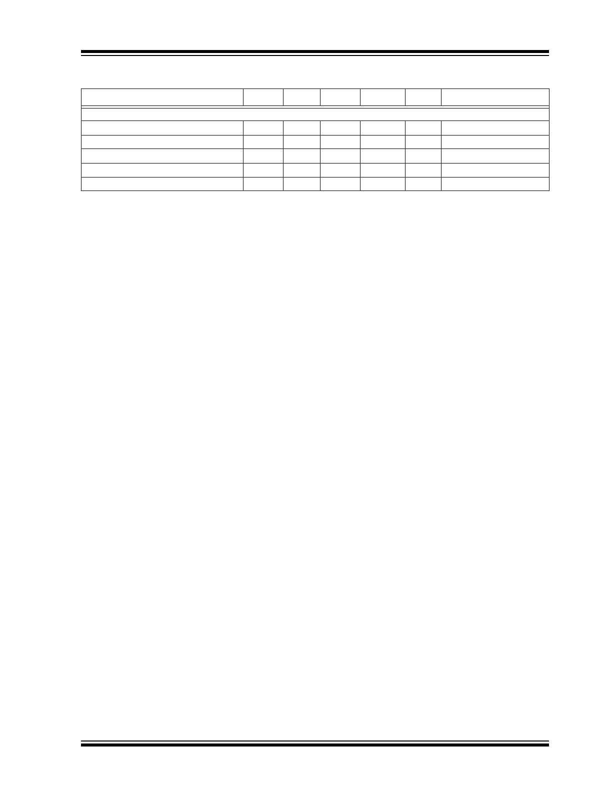
TABLE 2-1:
DSC6101/02/11/12/21/22/41/42/51/52/61/62 PIN FUNCTION TABLE (OUTPUT
FREQUENCY ≥1 MHZ)
Pin Number
Pin Name
Pin Type
Description
1
OE
I
Output Enable: H = Specified Frequency Output,
Note 1
L = Output is high impedance
STBY
Standby: H = Specified Frequency Output,
Note 1
L = Output is high impedance. Device is in low power
mode, supply current is at I
STBY
FS
Frequency Select: H = Output Frequency 1,
Note 2
L = Output Frequency 2
2
GND
Power
Power supply ground
3
Output
O
Oscillator clock output
4
VDD
Power
Power supply
TABLE 2-2:
DSC6183 PIN FUNCTION TABLE (OUTPUT FREQUENCY <1 MHZ)
Pin Number
Pin Name
Pin Type
Description
1
Output
O
Kilohertz Oscillator clock output
2
GND
Power
Power supply ground
3
DNC
DNC
Do Not Connect
4
VDD
Power
Power supply,
Note 1
2017 Microchip Technology Inc.
DS20005624B-page 7
DSC61XX
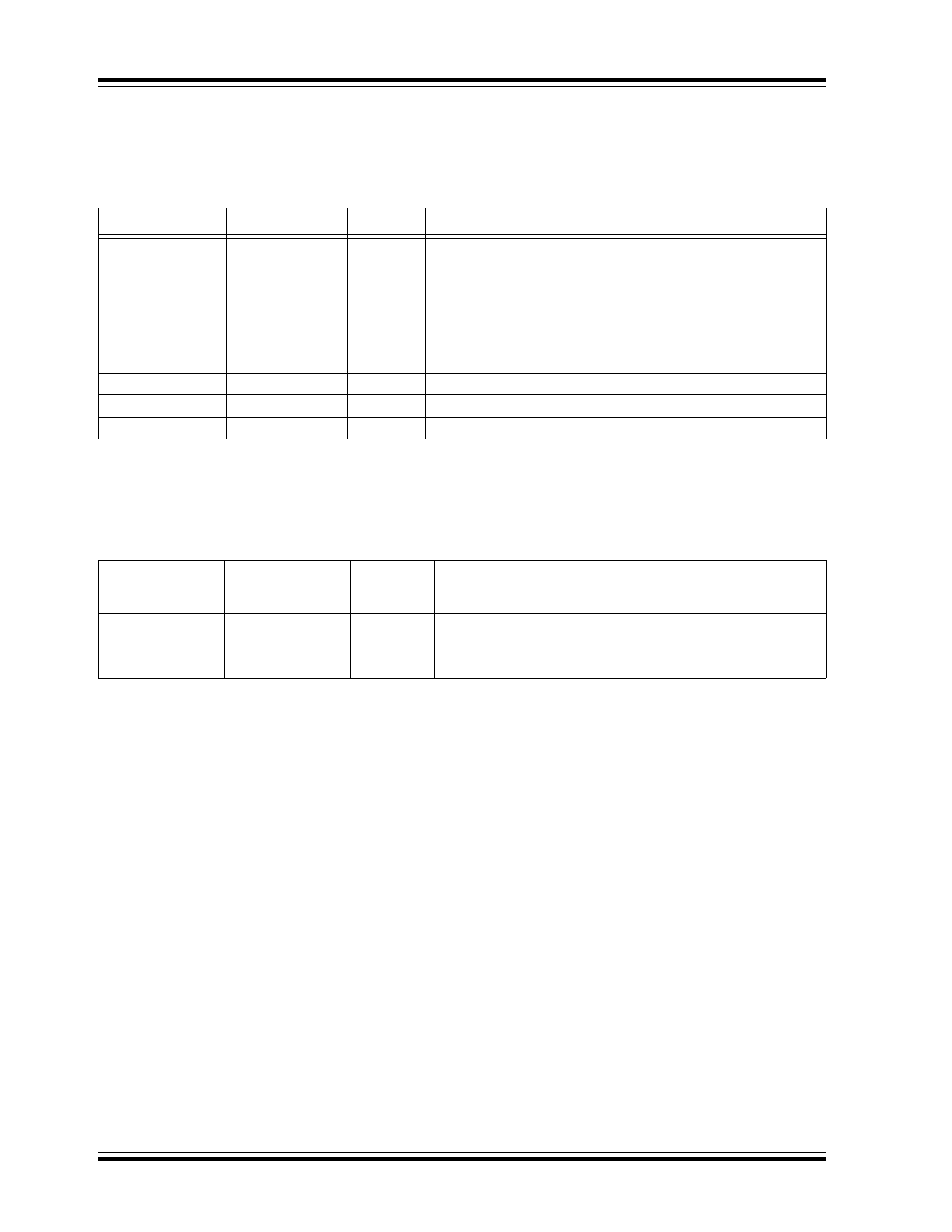
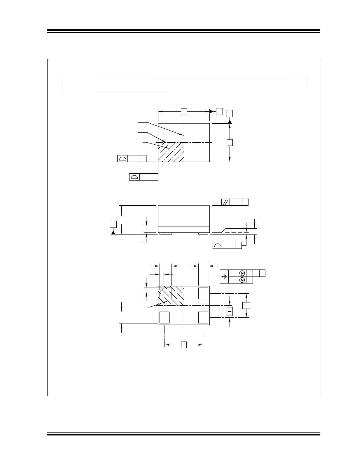
3.0
DIAGRAMS
FIGURE 3-1:
Output Waveform.
FIGURE 3-2:
Test Circuit.
FIGURE 3-3:
Recommended Board Layout.
V
OH
V
OL
V
IL
1/f
o
OUTPUT
ENABLE
t
DA
t
EN
t
F
t
R
V
IH
V
DD
0.1μF
4
3
1
2
V
DA
I
DD
C
L
VDD
C1
GND
Enable
Output
Via to GND Layer
Via to GND Layer
DSC61XX
DS20005624B-page 8
2017 Microchip Technology Inc.
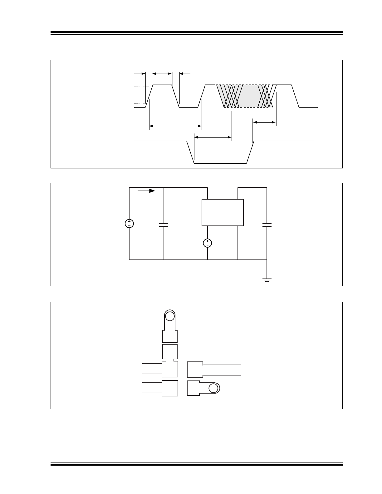
4.0
SOLDER REFLOW PROFILE
FIGURE 4-1:
Solder Reflow Profile.
60-180
Seconds
Tempera
ture (°C)
260°C
3°
C/sec max.
217°C
200°C
150°C
25°C
8 minutes max.
Pre-Heat
3°
C/sec max.
Reflow
Cool
Time
6
°C/sec max.
60-150
Seconds
20-40
Seconds
MSL 1 @ 260°C refer to JSTD-020C
Ramp-Up Rate (200°C to Peak Temp)
3°C/sec. max.
Preheat Time 150°C to 200°C
60 to 180 sec.
Time maintained above 217°C
60 to 150 sec.
Peak Temperature
255°C to 260°C
Time within 5°C of actual Peak
20 to 40 sec.
Ramp-Down Rate
6°C/sec. max.
Time 25°C to Peak Temperature
8 minutes max.
2017 Microchip Technology Inc.
DS20005624B-page 9
DSC61XX
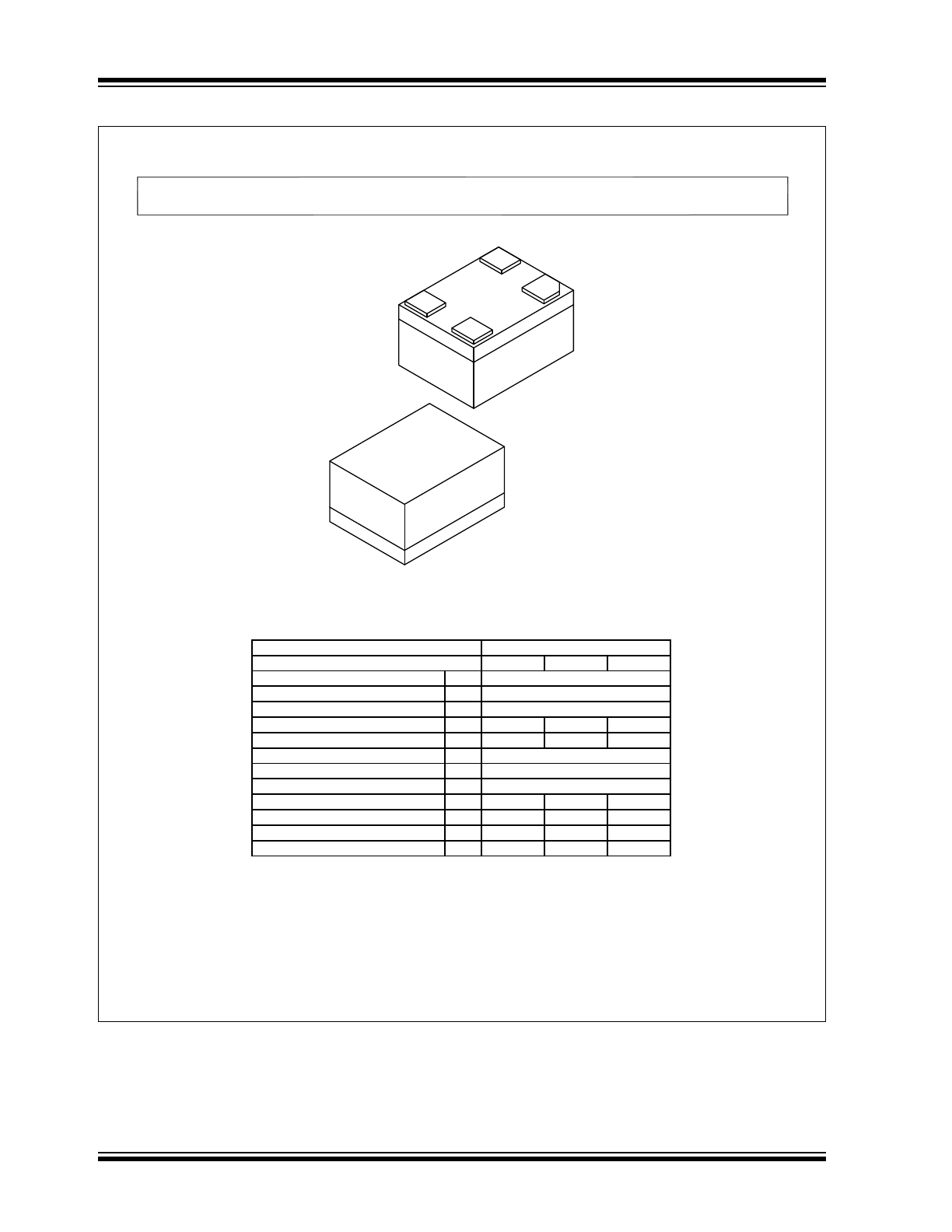
5.0
PACKAGING INFORMATION
4-Lead VFLGA 1.6 mm x 1.2 mm Package Outline
0.07
C A B
0.03
C
(DATUM B)
(DATUM A)
C
SEATING
PLANE
NOTE 1
1
2
N
TOP VIEW
SIDE VIEW
BOTTOM VIEW
NOTE 1
1
2
N
0.10 C
0.08 C
Microchip Technology Drawing C04-1199A Sheet 1 of 2
4X
For the most current package drawings, please see the Microchip Packaging Specification located at
http://www.microchip.com/packaging
Note:
4-Lead Very Thin Fine Pitch Land Grid Array (ARA) - 1.6x1.2 mm Body [VFLGA]
D
E
B
A
0.05 C
0.05 C
2X
2X
4X L
b2
e
CH
CH
A
(A3)
A1
e1
e1
2
3X b1
DSC61XX
DS20005624B-page 10
2017 Microchip Technology Inc.
4-Lead VFLGA 1.6 mm x 1.2 mm Package Outline
Microchip Technology Drawing C04-1199A Sheet 2 of 2
REF: Reference Dimension, usually without tolerance, for information purposes only.
BSC: Basic Dimension. Theoretically exact value shown without tolerances.
1.
2.
3.
Notes:
Pin 1 visual index feature may vary, but must be located within the hatched area.
Package is saw singulated
Dimensioning and tolerancing per ASME Y14.5M
4-Lead Very Thin Fine Pitch Land Grid Array (ARA) - 1.6x1.2 mm Body [VFLGA]
For the most current package drawings, please see the Microchip Packaging Specification located at
http://www.microchip.com/packaging
Note:
Number of Terminals
Overall Height
Overall Width
Terminal Length
Substrate Thickness (with Terminals)
Terminal Pitch
Standoff
Units
Dimension Limits
A1
A
b2
A3
e
L
E
N
1.20 BSC
0.20 REF
0.325
0.30
0.79
0.00
0.35
0.375
0.84
0.02
1.20 BSC
MILLIMETERS
MIN
NOM
4
0.425
0.40
0.89
0.05
MAX
CH
0.125
-
-
Terminal 1 Index Chamfer
Overall Length
D
1.60 BSC
Terminal Width
b1
0.25
0.30
0.35
Terminal Width
Terminal Pitch
e1
0.75 BSC