

SMSC UFX7000
Revision 1.4 (06-24-13)
DATASHEET
Datasheet
PRODUCT FEATURES
UFX7000
USB 3.0 Super-Speed Graphics
Controller with VGA, HDMI/DVI,
and Digital RGB Interfaces
Highlights
Single-Chip Super-Speed USB 3.0 Graphics Adapter
USB 3.0 and 2.0 Device Controllers with Integrated
USB 3.0 and 2.0 PHYs
Highly Efficient Compression Algorithm
Supports Uncompressed HD Quality Content in
USB 3.0 Mode
HDMI/DVI Display Connectivity via Integrated
HDMI/DVI Controller/PHY
VGA Display Connectivity via Integrated Video DAC
Support for External Display Interface IC’s via
Digital RGB Interface
High Performance DDR2 SDRAM Controller with
Integrated DDR2 PHY
Target Applications
USB to Video Adapters
Docking Stations, USB Port Replicators
Thin Clients
USB Monitors and Projectors
Embedded Systems
Features
USB 3.0 and 2.0 Device Controllers
— Fully compliant with Universal Serial Bus Specification
Revision 3.0
— Operates in SS (5 Gbps) and HS (480 Mbps) modes
— Supports Control, Bulk-Out, and Interrupt-In endpoints
— Supports vendor specific commands
— Integrated USB 3.0 and 2.0 PHYs
— Integrated USB termination pull-up/pull-down resistors
— Short circuit protection of USB differential signals
Graphics Subsystem
— Integrated HDMI/DVI Controller and PHY
– Complies with DVI specification v1.0
– Complies with HDMI specification v1.3
– S/PDIF and I
2
S inputs for HDMI audio
(2-channel uncompressed PCM)
– Master I
2
C interface for DDC connection
— Integrated Triple 10-bit Video DAC with VGA output
— Digital RGB Interface
– 12/15-bit double data rate digital RGB
– 24-bit single data rate digital RGB
— Supports up to 2048x1152 (QWXGA) with 32-bit color
— 8-bit and 16-bit color support
— Supports display cloning and extending
— Standard and wide screen aspect ratios
— Complies with VESA auto display identification
— Gamma correction
— Color Look-Up Table (CLUT)
— Triple-buffered animations
— Graphics Engine
– Optimized algorithms for static and dynamic content
– I
2
C controller
DDR2 SDRAM Controller
— 16-bit data bus, 13-bit address bus
— JEDEC DDR2 compliant (JESD79-2E)
— Integrated DDR2 SDRAM PHY
Power
— Reduced power operating modes
— Supports bus-powered and self-powered operation
Miscellaneous Features
— Optional EEPROM controller
— IEEE 1149.1 (JTAG) boundary scan TAP controller
Software
— Microsoft Windows® XP/Vista/7 drivers
Packaging & Environmental
— 225-ball LFBGA, RoHS compliant package
— Commercial temperature range (0°C to +70°C)

Order Number:
UFX7000-VE for 225-Ball LFBGA RoHS Compliant Package (0 TO +70°C Temp Range)
This product meets the halogen maximum concentration values per IEC61249-2-21
For RoHS compliance and environmental information, please visit
www.smsc.com/rohs
Please contact your SMSC sales representative for additional documentation related to this product
such as application notes, anomaly sheets, and design guidelines.
Copyright © 2013 SMSC or its subsidiaries. All rights reserved.
Circuit diagrams and other information relating to SMSC products are included as a means of illustrating typical applications. Consequently, complete information sufficient for
construction purposes is not necessarily given. Although the information has been checked and is believed to be accurate, no responsibility is assumed for inaccuracies. SMSC
reserves the right to make changes to specifications and product descriptions at any time without notice. Contact your local SMSC sales office to obtain the latest specifications
before placing your product order. The provision of this information does not convey to the purchaser of the described semiconductor devices any licenses under any patent
rights or other intellectual property rights of SMSC or others. All sales are expressly conditional on your agreement to the terms and conditions of the most recently dated
version of SMSC's standard Terms of Sale Agreement dated before the date of your order (the "Terms of Sale Agreement"). The product may contain design defects or errors
known as anomalies which may cause the product's functions to deviate from published specifications. Anomaly sheets are available upon request. SMSC products are not
designed, intended, authorized or warranted for use in any life support or other application where product failure could cause or contribute to personal injury or severe property
damage. Any and all such uses without prior written approval of an Officer of SMSC and further testing and/or modification will be fully at the risk of the customer. Copies of
this document or other SMSC literature, as well as the Terms of Sale Agreement, may be obtained by visiting SMSC’s website at http://www.smsc.com. SMSC is a registered
trademark of Standard Microsystems Corporation (“SMSC”). Product names and company names are the trademarks of their respective holders.
The MIcrochip name and logo, and the Microchip logo are registered trademarks of MIcrochip Technology Incorporated in the U.S.A. and other countries.
SMSC DISCLAIMS AND EXCLUDES ANY AND ALL WARRANTIES, INCLUDING WITHOUT LIMITATION ANY AND ALL IMPLIED WARRANTIES OF MERCHANTABILITY,
FITNESS FOR A PARTICULAR PURPOSE, TITLE, AND AGAINST INFRINGEMENT AND THE LIKE, AND ANY AND ALL WARRANTIES ARISING FROM ANY COURSE
OF DEALING OR USAGE OF TRADE. IN NO EVENT SHALL SMSC BE LIABLE FOR ANY DIRECT, INCIDENTAL, INDIRECT, SPECIAL, PUNITIVE, OR CONSEQUENTIAL
DAMAGES; OR FOR LOST DATA, PROFITS, SAVINGS OR REVENUES OF ANY KIND; REGARDLESS OF THE FORM OF ACTION, WHETHER BASED ON CONTRACT;
TORT; NEGLIGENCE OF SMSC OR OTHERS; STRICT LIABILITY; BREACH OF WARRANTY; OR OTHERWISE; WHETHER OR NOT ANY REMEDY OF BUYER IS HELD
TO HAVE FAILED OF ITS ESSENTIAL PURPOSE, AND WHETHER OR NOT SMSC HAS BEEN ADVISED OF THE POSSIBILITY OF SUCH DAMAGES.
USB 3.0 Super-Speed Graphics Controller with VGA, HDMI/DVI, and Digital RGB Interfaces
Datasheet
Revision 1.4 (06-24-13)
2
SMSC UFX7000
DATASHEET

USB 3.0 Super-Speed Graphics Controller with VGA, HDMI/DVI, and Digital RGB Interfaces
Datasheet
SMSC UFX7000
3
Revision 1.4 (06-24-13)
DATASHEET
Table of Contents
Chapter 1 Introduction . . . . . . . . . . . . . . . . . . . . . . . . . . . . . . . . . . . . . . . . . . . . . . . . . . . . . . . . 6
1.1
USB Device Controller . . . . . . . . . . . . . . . . . . . . . . . . . . . . . . . . . . . . . . . . . . . . . . . . . . . . . . . . . . . 6
1.2
Graphics Subsystem. . . . . . . . . . . . . . . . . . . . . . . . . . . . . . . . . . . . . . . . . . . . . . . . . . . . . . . . . . . . . 7
1.3
DDR2 SDRAM Interface . . . . . . . . . . . . . . . . . . . . . . . . . . . . . . . . . . . . . . . . . . . . . . . . . . . . . . . . . . 7
1.4
Peripherals . . . . . . . . . . . . . . . . . . . . . . . . . . . . . . . . . . . . . . . . . . . . . . . . . . . . . . . . . . . . . . . . . . . . 7
Chapter 2 Pin Description and Configuration . . . . . . . . . . . . . . . . . . . . . . . . . . . . . . . . . . . . . . 8
2.1
Pin Assignments . . . . . . . . . . . . . . . . . . . . . . . . . . . . . . . . . . . . . . . . . . . . . . . . . . . . . . . . . . . . . . . 25
2.2
Buffer Types . . . . . . . . . . . . . . . . . . . . . . . . . . . . . . . . . . . . . . . . . . . . . . . . . . . . . . . . . . . . . . . . . . 28
Chapter 3 Power Connections . . . . . . . . . . . . . . . . . . . . . . . . . . . . . . . . . . . . . . . . . . . . . . . . . . 29
Chapter 4 EEPROM. . . . . . . . . . . . . . . . . . . . . . . . . . . . . . . . . . . . . . . . . . . . . . . . . . . . . . . . . . 30
4.1
EEPROM Format . . . . . . . . . . . . . . . . . . . . . . . . . . . . . . . . . . . . . . . . . . . . . . . . . . . . . . . . . . . . . . 30
4.2
EEPROM Defaults . . . . . . . . . . . . . . . . . . . . . . . . . . . . . . . . . . . . . . . . . . . . . . . . . . . . . . . . . . . . . 37
4.3
EEPROM Auto-Load. . . . . . . . . . . . . . . . . . . . . . . . . . . . . . . . . . . . . . . . . . . . . . . . . . . . . . . . . . . . 37
4.4
Customized Operation Without EEPROM . . . . . . . . . . . . . . . . . . . . . . . . . . . . . . . . . . . . . . . . . . . 37
Chapter 5 Operational Characteristics. . . . . . . . . . . . . . . . . . . . . . . . . . . . . . . . . . . . . . . . . . . 38
5.1
Absolute Maximum Ratings*. . . . . . . . . . . . . . . . . . . . . . . . . . . . . . . . . . . . . . . . . . . . . . . . . . . . . . 38
5.2
Operating Conditions** . . . . . . . . . . . . . . . . . . . . . . . . . . . . . . . . . . . . . . . . . . . . . . . . . . . . . . . . . . 38
5.3
Package Thermal Specifications . . . . . . . . . . . . . . . . . . . . . . . . . . . . . . . . . . . . . . . . . . . . . . . . . . 39
5.4
Current Consumption . . . . . . . . . . . . . . . . . . . . . . . . . . . . . . . . . . . . . . . . . . . . . . . . . . . . . . . . . . . 39
5.4.1
SUSPEND Power State. . . . . . . . . . . . . . . . . . . . . . . . . . . . . . . . . . . . . . . . . . . . . . . . . . 39
5.4.2
Operational . . . . . . . . . . . . . . . . . . . . . . . . . . . . . . . . . . . . . . . . . . . . . . . . . . . . . . . . . . . 40
5.5
DC Specifications . . . . . . . . . . . . . . . . . . . . . . . . . . . . . . . . . . . . . . . . . . . . . . . . . . . . . . . . . . . . . . 41
5.6
AC Specifications . . . . . . . . . . . . . . . . . . . . . . . . . . . . . . . . . . . . . . . . . . . . . . . . . . . . . . . . . . . . . . 42
5.6.1
Power Sequence Timing . . . . . . . . . . . . . . . . . . . . . . . . . . . . . . . . . . . . . . . . . . . . . . . . . 43
5.6.2
Power-On Reset Timing . . . . . . . . . . . . . . . . . . . . . . . . . . . . . . . . . . . . . . . . . . . . . . . . . 44
5.6.3
Reset Timing . . . . . . . . . . . . . . . . . . . . . . . . . . . . . . . . . . . . . . . . . . . . . . . . . . . . . . . . . . 45
5.6.4
Video DAC Timing . . . . . . . . . . . . . . . . . . . . . . . . . . . . . . . . . . . . . . . . . . . . . . . . . . . . . . 45
5.6.5
Digital RGB Timing . . . . . . . . . . . . . . . . . . . . . . . . . . . . . . . . . . . . . . . . . . . . . . . . . . . . . 46
5.6.6
EEPROM Timing . . . . . . . . . . . . . . . . . . . . . . . . . . . . . . . . . . . . . . . . . . . . . . . . . . . . . . . 48
5.6.7
JTAG Timing . . . . . . . . . . . . . . . . . . . . . . . . . . . . . . . . . . . . . . . . . . . . . . . . . . . . . . . . . . 49
5.7
Clock Circuit . . . . . . . . . . . . . . . . . . . . . . . . . . . . . . . . . . . . . . . . . . . . . . . . . . . . . . . . . . . . . . . . . . 50
Chapter 6 Package Outline . . . . . . . . . . . . . . . . . . . . . . . . . . . . . . . . . . . . . . . . . . . . . . . . . . . . 51
6.1
225-LFBGA Package . . . . . . . . . . . . . . . . . . . . . . . . . . . . . . . . . . . . . . . . . . . . . . . . . . . . . . . . . . . 51
Chapter 7 Datasheet Revision History . . . . . . . . . . . . . . . . . . . . . . . . . . . . . . . . . . . . . . . . . . . 53

USB 3.0 Super-Speed Graphics Controller with VGA, HDMI/DVI, and Digital RGB Interfaces
Datasheet
Revision 1.4 (06-24-13)
4
SMSC UFX7000
DATASHEET
List of Figures
Figure 1.1 Internal Block Diagram. . . . . . . . . . . . . . . . . . . . . . . . . . . . . . . . . . . . . . . . . . . . . . . . . . . . . . . 6
Figure 2.1 Pin Assignments (TOP VIEW) . . . . . . . . . . . . . . . . . . . . . . . . . . . . . . . . . . . . . . . . . . . . . . . . . 8
Figure 3.1 Power Connections . . . . . . . . . . . . . . . . . . . . . . . . . . . . . . . . . . . . . . . . . . . . . . . . . . . . . . . . 29
Figure 5.1 Power-On Timing . . . . . . . . . . . . . . . . . . . . . . . . . . . . . . . . . . . . . . . . . . . . . . . . . . . . . . . . . . 43
Figure 5.1 nRESET Power-On Timing . . . . . . . . . . . . . . . . . . . . . . . . . . . . . . . . . . . . . . . . . . . . . . . . . . 44
Figure 5.1 nRESET Timing . . . . . . . . . . . . . . . . . . . . . . . . . . . . . . . . . . . . . . . . . . . . . . . . . . . . . . . . . . . 45
Figure 5.2 Digital RGB Timing - DDR Mode . . . . . . . . . . . . . . . . . . . . . . . . . . . . . . . . . . . . . . . . . . . . . . 46
Figure 5.3 Digital RGB Timing - SDR Mode . . . . . . . . . . . . . . . . . . . . . . . . . . . . . . . . . . . . . . . . . . . . . . 47
Figure 5.4 EEPROM Timing . . . . . . . . . . . . . . . . . . . . . . . . . . . . . . . . . . . . . . . . . . . . . . . . . . . . . . . . . . 48
Figure 5.5 JTAG Timing . . . . . . . . . . . . . . . . . . . . . . . . . . . . . . . . . . . . . . . . . . . . . . . . . . . . . . . . . . . . . 49
Figure 6.1 225-LFBGA Package Definition . . . . . . . . . . . . . . . . . . . . . . . . . . . . . . . . . . . . . . . . . . . . . . . 51
Figure 6.2 225-LFBGA Package Ball Detail . . . . . . . . . . . . . . . . . . . . . . . . . . . . . . . . . . . . . . . . . . . . . . 51
Figure 6.1 225-LFBGA Recommended PCB Land Pattern. . . . . . . . . . . . . . . . . . . . . . . . . . . . . . . . . . . 52

USB 3.0 Super-Speed Graphics Controller with VGA, HDMI/DVI, and Digital RGB Interfaces
Datasheet
SMSC UFX7000
5
Revision 1.4 (06-24-13)
DATASHEET
List Of Tables
Table 2.1 USB Pins . . . . . . . . . . . . . . . . . . . . . . . . . . . . . . . . . . . . . . . . . . . . . . . . . . . . . . . . . . . . . . . . . . 9
Table 2.2 Digital RGB Pins . . . . . . . . . . . . . . . . . . . . . . . . . . . . . . . . . . . . . . . . . . . . . . . . . . . . . . . . . . . 10
Table 2.3 RGB / DDR Mode Mapping Table . . . . . . . . . . . . . . . . . . . . . . . . . . . . . . . . . . . . . . . . . . . . . . 15
Table 2.4 VDAC Pins. . . . . . . . . . . . . . . . . . . . . . . . . . . . . . . . . . . . . . . . . . . . . . . . . . . . . . . . . . . . . . . . 16
Table 2.5 DDR2 Memory Pins . . . . . . . . . . . . . . . . . . . . . . . . . . . . . . . . . . . . . . . . . . . . . . . . . . . . . . . . . 18
Table 2.6 HDMI Pins . . . . . . . . . . . . . . . . . . . . . . . . . . . . . . . . . . . . . . . . . . . . . . . . . . . . . . . . . . . . . . . . 19
Table 2.7 EEPROM Pins . . . . . . . . . . . . . . . . . . . . . . . . . . . . . . . . . . . . . . . . . . . . . . . . . . . . . . . . . . . . . 20
Table 2.8 JTAG Pins . . . . . . . . . . . . . . . . . . . . . . . . . . . . . . . . . . . . . . . . . . . . . . . . . . . . . . . . . . . . . . . . 21
Table 2.9 Miscellaneous Pins . . . . . . . . . . . . . . . . . . . . . . . . . . . . . . . . . . . . . . . . . . . . . . . . . . . . . . . . . 21
Table 2.10 I/O Power Pins, Core Power Pins, and Ground Pins. . . . . . . . . . . . . . . . . . . . . . . . . . . . . . . . 23
Table 2.11 No-Connect Pins . . . . . . . . . . . . . . . . . . . . . . . . . . . . . . . . . . . . . . . . . . . . . . . . . . . . . . . . . . . 24
Table 2.12 225-LFBGA Package Pin Assignments . . . . . . . . . . . . . . . . . . . . . . . . . . . . . . . . . . . . . . . . . . 25
Table 2.13 Buffer Types . . . . . . . . . . . . . . . . . . . . . . . . . . . . . . . . . . . . . . . . . . . . . . . . . . . . . . . . . . . . . . 28
Table 4.1 EEPROM Format. . . . . . . . . . . . . . . . . . . . . . . . . . . . . . . . . . . . . . . . . . . . . . . . . . . . . . . . . . . 31
Table 4.2 Configuration Flags 0. . . . . . . . . . . . . . . . . . . . . . . . . . . . . . . . . . . . . . . . . . . . . . . . . . . . . . . . 34
Table 4.3 Configuration Flags 1. . . . . . . . . . . . . . . . . . . . . . . . . . . . . . . . . . . . . . . . . . . . . . . . . . . . . . . . 35
Table 4.4 Configuration Flags 2. . . . . . . . . . . . . . . . . . . . . . . . . . . . . . . . . . . . . . . . . . . . . . . . . . . . . . . . 36
Table 4.5 Configuration Flags 3. . . . . . . . . . . . . . . . . . . . . . . . . . . . . . . . . . . . . . . . . . . . . . . . . . . . . . . . 36
Table 4.6 EEPROM Defaults . . . . . . . . . . . . . . . . . . . . . . . . . . . . . . . . . . . . . . . . . . . . . . . . . . . . . . . . . . 37
Table 5.1 Package Thermal Parameters . . . . . . . . . . . . . . . . . . . . . . . . . . . . . . . . . . . . . . . . . . . . . . . . . 39
Table 5.2 SUSPEND Supply Current . . . . . . . . . . . . . . . . . . . . . . . . . . . . . . . . . . . . . . . . . . . . . . . . . . . 39
Table 5.3 Typical Super-Speed Operational Supply Current (mA) . . . . . . . . . . . . . . . . . . . . . . . . . . . . . 40
Table 5.4 Typical High-Speed Operational Supply Current (mA) . . . . . . . . . . . . . . . . . . . . . . . . . . . . . . 40
Table 5.5 I/O Buffer Characteristics. . . . . . . . . . . . . . . . . . . . . . . . . . . . . . . . . . . . . . . . . . . . . . . . . . . . . 41
Table 5.6 Video DAC - DC Characteristics . . . . . . . . . . . . . . . . . . . . . . . . . . . . . . . . . . . . . . . . . . . . . . . 42
Table 5.7 Power-On Timing Values. . . . . . . . . . . . . . . . . . . . . . . . . . . . . . . . . . . . . . . . . . . . . . . . . . . . . 43
Table 5.8 nRESET Power-On Timing Values . . . . . . . . . . . . . . . . . . . . . . . . . . . . . . . . . . . . . . . . . . . . . 44
Table 5.9 nRESET Timing Values . . . . . . . . . . . . . . . . . . . . . . . . . . . . . . . . . . . . . . . . . . . . . . . . . . . . . . 45
Table 5.10 Video DAC - AC Characteristics . . . . . . . . . . . . . . . . . . . . . . . . . . . . . . . . . . . . . . . . . . . . . . . 45
Table 5.11 Digital RGB Timing Values - DDR Mode . . . . . . . . . . . . . . . . . . . . . . . . . . . . . . . . . . . . . . . . . 46
Table 5.12 Digital RGB Timing Values - SDR Mode . . . . . . . . . . . . . . . . . . . . . . . . . . . . . . . . . . . . . . . . . 47
Table 5.13 EEPROM Timing Values . . . . . . . . . . . . . . . . . . . . . . . . . . . . . . . . . . . . . . . . . . . . . . . . . . . . . 48
Table 5.14 JTAG Timing Values . . . . . . . . . . . . . . . . . . . . . . . . . . . . . . . . . . . . . . . . . . . . . . . . . . . . . . . . 49
Table 5.15 Crystal Specifications . . . . . . . . . . . . . . . . . . . . . . . . . . . . . . . . . . . . . . . . . . . . . . . . . . . . . . . 50
Table 6.1 225-LFBGA Package Parameters . . . . . . . . . . . . . . . . . . . . . . . . . . . . . . . . . . . . . . . . . . . . . . 52
Table 7.1 Customer Revision History . . . . . . . . . . . . . . . . . . . . . . . . . . . . . . . . . . . . . . . . . . . . . . . . . . . 53
USB 3.0 Super-Speed Graphics Controller with VGA, HDMI/DVI, and Digital RGB Interfaces
Datasheet
Revision 1.4 (06-24-13)
6
SMSC UFX7000
DATASHEET
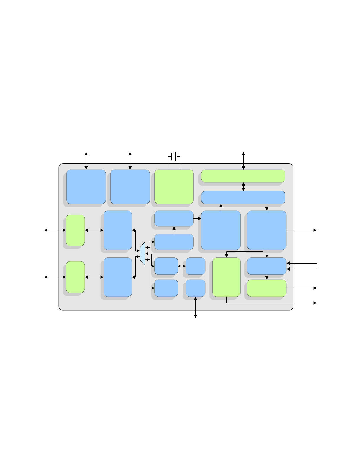
Chapter 1 Introduction
The UFX7000 is a high performance USB 3.0 graphics adapter with multiple graphics interfaces. The
UFX7000 is an ideal solution for extending a PC workspace to an additional monitor without the need
for an additional internal graphics card. With applications ranging from docking stations, USB port
replicators, USB monitors/projectors, and embedded systems, the UFX7000 is targeted as a high
performance, low cost USB-to-graphics solution.
The UFX7000 contains integrated USB 3.0 and 2.0 Device Controllers, USB 3.0 and 2.0 PHYs, a USB
Bulk-Out Controller, Control Endpoint, Interrupt-In Endpoint, DDR2 SDRAM Controller/PHY, Graphics
Engine, HDMI/DVI Controller/PHY, Video DAC, TAP Controller, EEPROM Controller, and I
2
C
Controller.
Figure 1.1
details an internal block diagram of the UFX7000.
1.1
USB Device Controller
The USB Device Controller is fully compliant with the USB 3.0 Specification, enabling the device to
operate in Super-Speed (5 Gbps) or Hi-Speed (480 Mbps) mode. Integrated USB 3.0 and 2.0 PHYs
are provided on the USB port.
The controller implements three USB endpoints: Control, Bulk-Out, and Interrupt-In. The Bulk-Out
endpoint allows for uncompressed or compressed graphics data reception from the USB port. The USB
Bulk-Out Controller collects the graphics information and transfers it to the Graphics Engine.
Implementation of vendor-specific commands allows for access to the device System Control and
Status Registers (SCSRs).
Figure 1.1 Internal Block Diagram
UFX7000
JTAG
DDR2 PHY
DDR2 Controller
(DCTL)
USB Bulk Ctl
(URX)
EEPROM
Controller
PLLs
TAP
Controller
EEPROM
DDR2 SDRAM
Graphics
Engine
(GPH)
Control
Endpoint
SCSRs
HDMI/DVI
Video
DAC
HDMI PHY
HDMI/DVI
Controller
VGA
MU
X
Digital RGB
I
2
C
Controller
I
2
C
FIFO Ctl
(FCT)
USB
3.0
PHY
USB
USB 2.0
Device
Ctrl
(UDC 2.0)
USB 3.0
Device
Ctrl
(UDC 3.0)
Display
Controller
(DISP)
USB
2.0
PHY
USB
Interrupt
Endpoint
S/PDIF
I
2
S

USB 3.0 Super-Speed Graphics Controller with VGA, HDMI/DVI, and Digital RGB Interfaces
Datasheet
SMSC UFX7000
7
Revision 1.4 (06-24-13)
DATASHEET
1.2
Graphics Subsystem
The Graphics Subsystem consists of the following main blocks: the Graphics Engine, Display
Controller, HDMI/DVI Controller/PHY, Video DAC, and the Digital RGB Interface. Together, these
blocks support high definition resolutions of up to 2048x1152 (QWXGA) with 32-bit true color in both
standard and wide screen aspect ratios. The HDMI/DVI interface is compliant with the HDMI v1.3 and
DVI v1.0 specifications and supports 2-channel uncompressed PCM audio via a S/PDIF or I
2
S input.
The Display Controller also supports 8-bit and 16-bit color, gamma correction, Color Look-Up Table
(CLUT) and triple-buffered animations. The DDC2B/EDID VESA standard is supported, allowing the
host OS and device drivers to query the monitor’s frequency, resolution, and other features for true
plug-and-play and intelligent mode setting capabilities.
Once the graphics data has been received via the USB Bulk-Out Controller, it is sent to the Graphics
Engine. If the data is compressed, the Graphics Engine decompresses it via algorithms that have been
optimized for speed and quality. The device’s decompression algorithms have been designed to work
seamlessly with the compression algorithms utilized in the software device drivers.
The graphics data is then transferred to the SDRAM via the DDR2 SDRAM Controller. The Display
Controller generates all display and interface timing signals, retrieves the graphics data from the DDR2
SDRAM, and sends it to the HDMI/DVI Controller/PHY, Video DAC, or Digital RGB Interface.
The Digital RGB Interface may be used to connect external display interface IC’s (e.g., DisplayPort,
etc.) via the provided RGB data channel busses and control signals. The Digital RGB Interface
supports two modes of operation: 24-bit single data rate mode and 12/15-bit double data rate mode.
24-bit mode is single edge triggered and utilizes the full 24-bit data bus width. The 12/15-bit mode is
triggered on both clock edges and utilizes 12/15-bits of the data bus width.
1.3
DDR2 SDRAM Interface
The UFX7000 provides a full JEDEC compliant (JESD79-2E) DDR2 SDRAM Controller and PHY for
interfacing to external DDR2 SDRAM. The DDR2 SDRAM interface is comprised of JEDEC standard
1.8V I/O signals grouped into control signals, a 16-bit data bus, and a 13-bit address bus.
The DDR2 SDRAM Controller transfers the graphics data in and out of external SDRAM through the
DDR2 SDRAM PHY. External SDRAM is used as storage for the graphics and acts a a buffer between
the Graphics Engine and Display Controller.
1.4
Peripherals
The UFX7000 also contains an EEPROM Controller, I
2
C Controller, and TAP Controller.
The EEPROM Controller allows connection to an external EEPROM for automatic loading of static
configuration data upon power-on, pin reset, or software reset. The EEPROM can be configured to
load USB descriptors and USB device configuration.
The integrated IEEE 1149.1 compliant TAP controller provides boundary scan via JTAG.
USB 3.0 Super-Speed Graphics Controller with VGA, HDMI/DVI, and Digital RGB Interfaces
Datasheet
Revision 1.4 (06-24-13)
8
SMSC UFX7000
DATASHEET
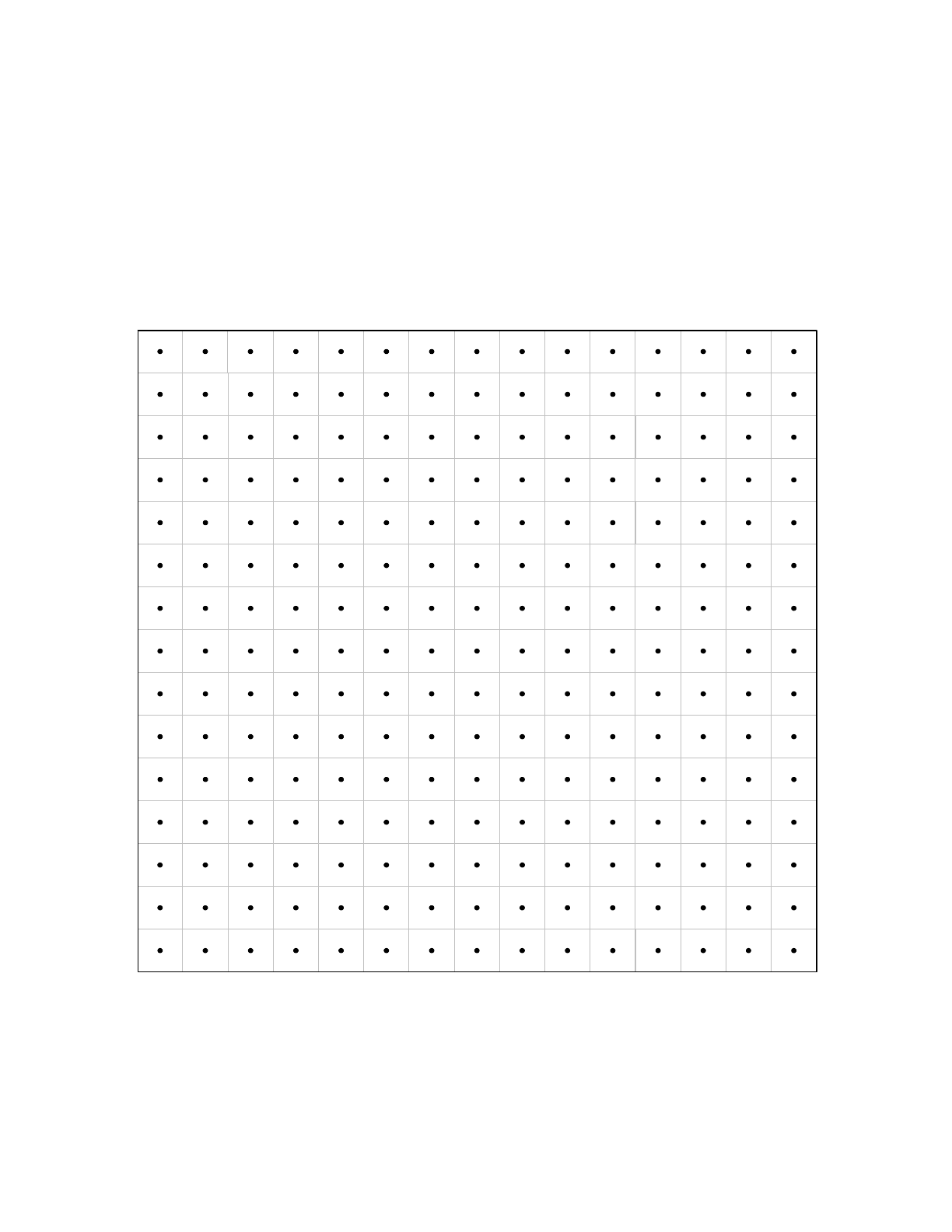
Chapter 2 Pin Description and Configuration
Figure 2.1 Pin Assignments (TOP VIEW)
nDDRDQS0
DDRDQ5
DDRDQ0
VDD18DDR
VDD18DDR
DDRDQ3
nDDRWE
DDRA10
DDRA3
DDRA9
DDRCK
nDDRCAS
DDRA2
VDD18DDR
VSS
DDRFIFOWE_OUT
DDRDQ7
DDRDQ12
DDRDQS0
DDRDM0
VDD18DDR
DDRDQ4
DDRCKE
DDRBA0
DDRA7
DDRA12
nDDRCK
nDDRCS
DDRA6
DDRA4
TX2P
DDRVREF0
DDRDQ11
DDRDQ9
DDRDQ2
DDRDQ6
DDRDQ1
DDRVREF2
DDRBA1
DDRA1
DDRA5
nDDRRAS
VDD18DDR
DDRA0
DDRODT
DDRA11
DDRA8
TX2N
DDRDQS1
DDRDM1
DDRDQ14
DDRDQ8
DDRDQ15
VDD18DDR
DDRDQ10
DDRVREF1
nDDRDQS1
TX1N
VSSUSB3
VDD33USB3
DDRDQ13
VSSHDMI
USB3TXDM
VDD12USB3
VSSUSB3
USB3RXDM
VSSUSB3
USB3TXDP
I2CSDA0
I2CSCL1/
GPIO28
USB3RXDP
USBDM
VBUS_DET
I2CSDA1/
GPIO27
NC
HPD
USBDP
USBRBIAS
VDATAB3/
VD4/GPIO19
VDD33USB
VDATAB2/
VD5/GPIO18
XI
VDD12USBPLL
NC
SYSPLLG
VDATAB6/
VD1/GPIO22
VDATAB5/
VD2/GPIO21
VDATAB1/
VD6/GPIO17
XO
SYSPLLP
VSYNC
VDATAG5/
VD8/GPIO13
VDATAG1/
VD10/GPIO9
EEDI
VDATAB7/
VD0/GPIO23
VCLK
VDATAR6/
GPIO6
VDATAB0/
GPIO16
VDD18DDR
VSS
VDD12USB3
REXT
I2CSCL0
AUDIO_DIS/
GPIO30
VDATAB4/
VD3/GPIO20
VDD18DDR
VDD18DDR
VDD18DDR
VDD18DDR
VDD18DDR
VDD18DDR
TX0N
TXCN
nVDACR
nVDACG
nVDACB
SPDIF/
I2SDATA/
GPIO26
EECLK
DDRFIFOWE_IN
VSS
EXTSWING
EEDO
VDATAR2/
VD15/GPIO2
nTRST
TMS
NC
LED/
I2SCLKALT1/
GPIO24
TX1P
HSYNC
nBLANK
nVCLK
VDATAG6/
VD7/GPIO14
VDATAG2/
GPIO10
VDATAR7/
VD12/GPIO7
VDATAR3/
VD14/GPIO3
VDATAR0/
I2SCLKALT0/
GPIO0
TCK
VDD12CORE
VSS
VDD12CORE
VSS
VDD12CORE
VDD18DDR
VSSHDMI
nEXTRST
nSW_MODE
nRESET
NC
EECS
MCLK/
GPIO25
VDACB
VDACG
VDACR
TXCP
TX0P
VDD12HDMI
VDD12HDMI
VDD18DDR
VDD12CORE
VSS
VSS
VDD12CORE
VSS
VDD12CORE
VDD33IO
VDD33IO
VDD12CORE
VSS
VSS
VSS
VDD33IO
VDATAG3/
GPIO11
VDATAR1/
GPIO1
WS/GPIO29
VDD33VDAC
VDD12HDMI
VSSHDMI
VSS
VSS
VSS
VSS
VSS
VSS
VSS
VSS
VDD12CORE
IREF
VSS
VSS
VSS
VSS
VSSVDAC
VDD33VDAC
VSS
VSS
VSS
VSS
VDD33VDAC
VDAC_HSYNC
VSS
VSS
VSS
VSS
VDACREF
VDD33IO
VSS
VDD12CORE
VSS
VDD12CORE
VDD33IO
TDI
VDD33IO
VDATAG4/
VD9/GPIO12
VDD33IO
VDATAR5/
GPIO5
VDD33IO
TDO
VDATAG7/
GPIO15
VDATAG0/
VD11/GPIO8
VDATAR4/
VD13/GPIO4
VSS
VDD12CORE
VSSVDAC
VDAC_VSYNC
INT
15
14
13
12
11
10
9
8
7
6
5
4
3
2
1
A
B
C
D
E
F
G
H
J
K
L
M
N
P
R
B
C
D
E
F
G
H
J
K
L
M
N
P
R
15
14
13
12
11
10
9
8
7
6
5
4
3
2
1
A
SMSC
UFX7000
225-LFBGA
TOP VIEW

USB 3.0 Super-Speed Graphics Controller with VGA, HDMI/DVI, and Digital RGB Interfaces
Datasheet
SMSC UFX7000
9
Revision 1.4 (06-24-13)
DATASHEET
Note 2.1
A 25MHz oscillator, or other single-ended clock source that meets the specifications in
Section 5.5, "DC Specifications," on page 41
and
Section 5.7, "Clock Circuit," on page 50
,
is required when utilizing the Digital RGB interface. Do not use a crystal when operating
in Digital RGB mode.
Table 2.1 USB Pins
NUM PINS
NAME
SYMBOL
BUFFER
TYPE
DESCRIPTION
1
USB
DMINUS
USBDM
AIO
USB Data Minus.
Note:
The functionality of this pin may be
swapped to USB DPLUS via the
Port
Swap
bit of
Configuration Flags 0
of the
EEPROM.
1
USB
DPLUS
USBDP
AIO
USB Data Plus.
Note:
The functionality of this pin may be
swapped to USB DMINUS via the
Port
Swap
bit of
Configuration Flags 0
of the
EEPROM.
1
External USB
Bias Resistor
USBRBIAS
AI
Used for setting HS transmit current level and on-
chip termination impedance. Connect to an
external 12K 1.0% resistor to ground.
1
Crystal Input
XI
ICLK
External 25 MHz crystal input.
Note:
This pin can also be driven by a single-
ended clock oscillator. When this
method is used, XO should be left
unconnected. (
Note 2.1
)
1
Crystal
Output
XO
OCLK
External 25 MHz crystal output.
1
USB3 RX
DMINUS
USB3RXDM
AIO
Super-Speed Differential Receive Minus.
1
USB3 RX
DPLUS
USB3RXDP
AIO
Super-Speed Differential Receive Plus.
1
USB3 TX
DMINUS
USB3TXDM
AIO
Super-Speed Differential Transmit Minus.
1
USB3 TX
DPLUS
USB3TXDP
AIO
Super-Speed Differential Transmit Plus.
1
USB3
External
Reference
Resistance
REXT
AI
Connect to an external 200 ohm 1.0% resistor to
ground.

USB 3.0 Super-Speed Graphics Controller with VGA, HDMI/DVI, and Digital RGB Interfaces
Datasheet
Revision 1.4 (06-24-13)
10
SMSC UFX7000
DATASHEET
Table 2.2 Digital RGB Pins
NUM PINS
NAME
SYMBOL
BUFFER
TYPE
DESCRIPTION
1
Video Clock
High
VCLK
RGB
Active high video clock.
1
Video Clock
Low
nVCLK
RGB
Active low video clock.
1
Horizontal
Sync
HSYNC
RGB
Video horizontal synchronization output.
1
Vertical Sync
VSYNC
RGB
Video vertical synchronization output.
1
Video
Blanking
nBLANK
RGB
Active low video blanking signal.
1
Blue Pixel
Data Channel
Bit 7
VDATAB7
RGB
Blue Pixel Video Data Bit 7, RGB Single Ended
Mode.
DDR RGB
Data 0
VD0
RGB
Used in RGB DDR Mode, refer to
Table 2.3
.
General
Purpose I/O
23
GPIO23
IS/O8/
OD8
(PU)
Note 2.2
This General Purpose I/O pin is fully
programmable as either a push-pull output, an
open-drain output, or a Schmitt-triggered input.
1
Blue Pixel
Data Channel
Bit 6
VDATAB6
RGB
Blue Pixel Video Data Bit 6, RGB Single Ended
Mode.
DDR RGB
Data 1
VD1
RGB
Used in RGB DDR Mode, refer to
Table 2.3
.
General
Purpose I/O
22
GPIO22
IS/O8/
OD8
(PU)
Note 2.2
This General Purpose I/O pin is fully
programmable as either a push-pull output, an
open-drain output, or a Schmitt-triggered input.
1
Blue Pixel
Data Channel
Bit 5
VDATAB5
RGB
Blue Pixel Video Data Bit 5, RGB Single Ended
Mode.
DDR RGB
Data 2
VD2
RGB
Used in RGB DDR Mode, refer to
Table 2.3
.
General
Purpose I/O
21
GPIO21
IS/O8/
OD8
(PU)
Note 2.2
This General Purpose I/O pin is fully
programmable as either a push-pull output, an
open-drain output, or a Schmitt-triggered input.
1
Blue Pixel
Data Channel
Bit 4
VDATAB4
RGB
Blue Pixel Video Data Bit 4, RGB Single Ended
Mode.
DDR RGB
Data 3
VD3
RGB
Used in RGB DDR Mode, refer to
Table 2.3
.
General
Purpose I/O
20
GPIO20
IS/O8/
OD8
(PU)
Note 2.2
This General Purpose I/O pin is fully
programmable as either a push-pull output, an
open-drain output, or a Schmitt-triggered input.