
2017 Microchip Technology Inc.
DS20005743A-page 1
UCS2114
Features
• Dual-Port Power Switches:
- 2.9V to 5.5V source voltage range
- 3.0A continuous current per V
BUS
port with
18 m
On resistance per switch
- Independent port power switch enable pins
- DUAL fault ALERT# active drain output pins
- Constant Current or Trip mode current
limiting behaviors
- Undervoltage and overvoltage lockout
- Back-drive, back-voltage protection
- Auto-recovery fault handling with low test
current
- BOOST# logic output to increase DC-DC
converter output under large load conditions
• SMBus 2.0/I
2
C Mode Features:
- Eight programmable current limits assignable
to each power switch
- Other SMBus addresses available upon
request
- Block read and block write
• Self-Contained Current Monitoring (No External
Sense Resistor Required)
• Fully Programmable Per-Port Charge Rationing
and Behaviors
• Configurable Per-Port BC1.2 V
BUS
Discharge
Function
• Wide Operating Temperature Range:
- –40°C to +105°C
Description
The UCS2114 is a dual USB port power switch
configuration that can provide 3.0A continuous current
(3.4A maximum) per V
BUS
port with precision
overcurrent limiting (OCL), port power switch enables,
auto-recovery fault handling, undervoltage and
overvoltage lockout, back-drive and back-voltage
protection, and thermal protection.
The UCS2114 is well-suited for both stand-alone and
applications having SMBus/I
2
C communications.
For applications with SMBus, the UCS2114 provides
per-port current monitoring and eight programmable
current limits per switch, ranging from 0.53A to 3.0A
continuous current (3.4A maximum). Per-port charge
rationing is also provided, ranging from 3.8 mAh
to
246.3 Ah.
In Stand-Alone mode, the UCS2114 provides eight
current limits for both switches, ranging from
0.53A + 0.53A to 3A + 3A total continuous current
(see
Table 1-1
).
Both power switches include an independent V
BUS
discharge function and Constant Current mode limiting
for BC1.2 applications.
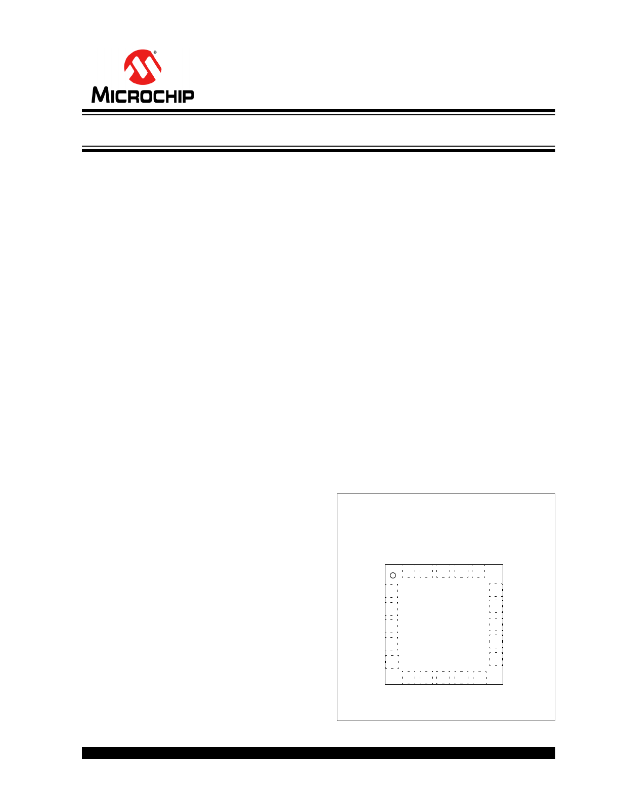
The UCS2114 is available in a 3x3 mm 20-pin VQFN
package.
Package Type
ALER
T#2
2
COMM_ILIM
V
BUS1
PWR_EN1
PWR_EN2
GND
V
S
BOOST#
V
S
V
DD
V
S
V
BUS2
ALER
T#
1
SMCL
K
SMDA
TA
GND
GND
20
1
19 18 17
3
4
14
13
12
11
6
7
8
9
5
10
15
16
V
BUS1
V
S
V
BUS2
UCS2114
3 x 3 VQFN
USB Dual-Port Power Switch and Current Monitor
UCS2114
DS20005743A-page 2
2017 Microchip Technology Inc.
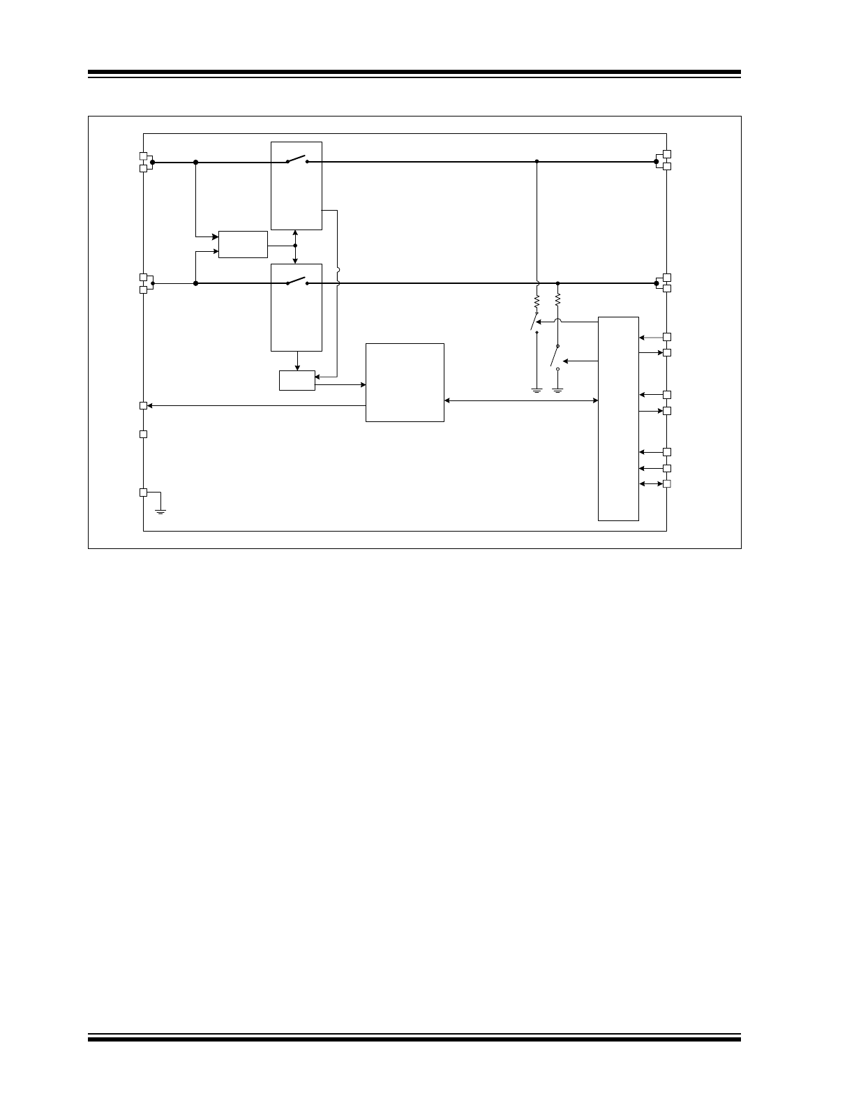
Block Diagram
Charger
Control,
Measurement,
OCL
In
te
rfa
ce Lo
gic
SMCLK
SMDATA
PWR_EN2
Power
Switch 2
Temp
ALERT#2
V
BUS
GND
COMM_ILIM
Power
Switch 1
V
BUS
V
S
UVLO,
OVLO
PWR_EN1
BOOST#
ALERT#1
V
BUS
discharge
V
DD
V
S
2017 Microchip Technology Inc.
DS20005743A-page 3
UCS2114
1.0
ELECTRICAL
CHARACTERISTICS
Absolute Maximum Ratings †
Voltage on V
DD
, V
S
and V
BUS
pins ...................................................................................................................–0.3 to 6V
Pull-Up Voltage (V
PULLUP
) .....................................................................................................................–0.3 to V
DD
+ 0.3
Port Power Switch Current ..................................................................................................................... Internally limited
Voltage on any Other Pin to Ground .................................................................................................. –0.3 to V
DD
+ 0.3V
Current on any Other Pin ..................................................................................................................................... ±10 mA
Operating Ambient Temperature Range ................................................................................................ –40°C to +105°C
Storage Temperature Range ................................................................................................................. –55°C to +150°C
† Notice: Stresses above those listed under “Maximum Ratings” may cause permanent damage to the device. This
is a stress rating only and functional operation of the device at those or any other conditions above those indicated in
the operation listings of this specification is not implied. Exposure to maximum rating conditions for extended periods
may affect device reliability.
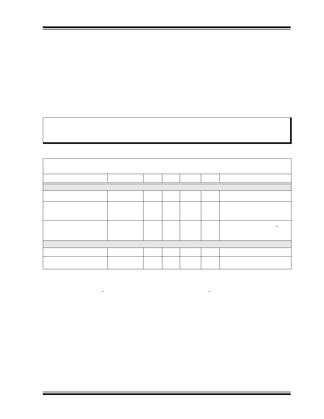
TABLE 1-1:
ELECTRICAL SPECIFICATIONS
Electrical Characteristics: Unless otherwise specified, V
DD
= 4.5V to 5.5V, V
S
= 2.9V to 5.5V,
V
PULLUP
= 3V to 5.5V, T
A
= –40°C to 105°C. All typical values at V
DD
= V
S
= 5V, T
A
= 27°C.
Characteristic
Symbol
Min.
Typ.
Max.
Unit
Conditions
Power and Interrupts - DC
Supply Voltage
V
DD
4.5
5
5.5
V
Supply Current in Active
(I
DD_ACT
+ I
S1_ACT
+ I
S2_ACT
)
I
ACTIVE
—
700
—
µA
Average current I
BUS
= 0 mA
Supply Current in Sleep
(I
DD_SLEEP
+ I
S1_SLEEP
+
I
S2_SLEEP
)
I
SLEEP
—
6
20
µA
Average current V
PULLUP
V
DD
Power-on Reset
V
DD
Low Threshold
V
DD_TH
—
4
4.3
V
V
DD
voltage increasing (
Note 1
)
V
DD
Low Hysteresis
V
DD_TH_HYST
—
500
600
mV
V
DD
voltage decreasing
(
Note 1
)
Note 1:
This parameter is characterized, not 100% tested.
2:
This parameter is ensured by design and not 100% tested.
3:
The current measurement full scale range maximum value is 3.4A. However, the UCS2114 cannot report values above
I
LIM
(if I
BUS_R2MIN
I
LIM
) or above I
BUS_R2MIN
(if I
BUS_R2MIN
> I
LIM
and I
LIM
1.6A).
UCS2114
DS20005743A-page 4
2017 Microchip Technology Inc.
I/O Pins - SMCLK, SMDATA, PWR_EN, ALERT#, BOOST# - DC Parameters
Output Low Voltage
V
OL
—
—
0.4
V
I
SINK_IO
= 8 mA
SMDATA, ALERT#, BOOST#
Input High Voltage
V
IH
2.0
—
—
V
PWR_EN, SMDATA, SMCLK
Input Low Voltage
V
IL
—
—
0.8
V
PWR_EN, SMDATA, SMCLK
Leakage Current
I
LEAK
—
—
±5
µA
Powered or unpowered
V
PULLUP
V
DD
T
A
< 85°C (
Note 1
)
Interrupt Pins - AC Parameters
ALERT# Pin Blanking Time
t
BLANK
—
25
—
ms
Blanking time, coming out of
reset
ALERT# Pin Interrupt
Masking Time
t
MASK
—
5
—
ms
BOOST# Pin Minimum
Assertion Time
t
BOOST_MAT
—
1
—
s
BOOST# Pin Assertion
Current
I
BOOST
—
1.9
—
A
SMBus/I
2
C Timing
Input Capacitance
C
IN
—
5
—
pF
Clock Frequency
f
SMB
10
—
400
kHz
Spike Suppression
t
SP
—
—
50
ns
Bus Free Time Stop to Start
t
BUF
1.3
—
—
µs
Start Setup Time
t
SU:STA
0.6
—
—
µs
Start Hold Time
t
HD:STA
0.6
—
—
µs
Stop Setup Time
t
SU:STO
0.6
—
—
µs
Data Hold Time
t
HD:DAT
0
—
—
µs
When transmitting to the master
Data Hold Time
t
HD:DAT
0.3
—
—
µs
When receiving from the master
Data Setup Time
t
SU:DAT
0.6
—
—
µs
Clock Low Period
t
LOW
1.3
—
—
µs
Clock High Period
t
HIGH
0.6
—
—
µs
Clock/Data Fall Time
t
FALL
—
—
300
ns
Min. = 20+0.1C
LOAD
ns
(
Note 1
)
Clock/Data Rise Time
t
RISE
—
—
300
ns
Min. = 20+0.1C
LOAD
ns
(
Note 1
)
Capacitive Load
C
LOAD
—
—
400
pF
Per bus line (
Note 1
)
Time Out
t
TIMEOUT
25
—
35
ms
Disabled by default (
Note 1
)
Idle Reset
t
IDLE_RESET
350
—
—
µs
Disabled by default (
Note 1
)
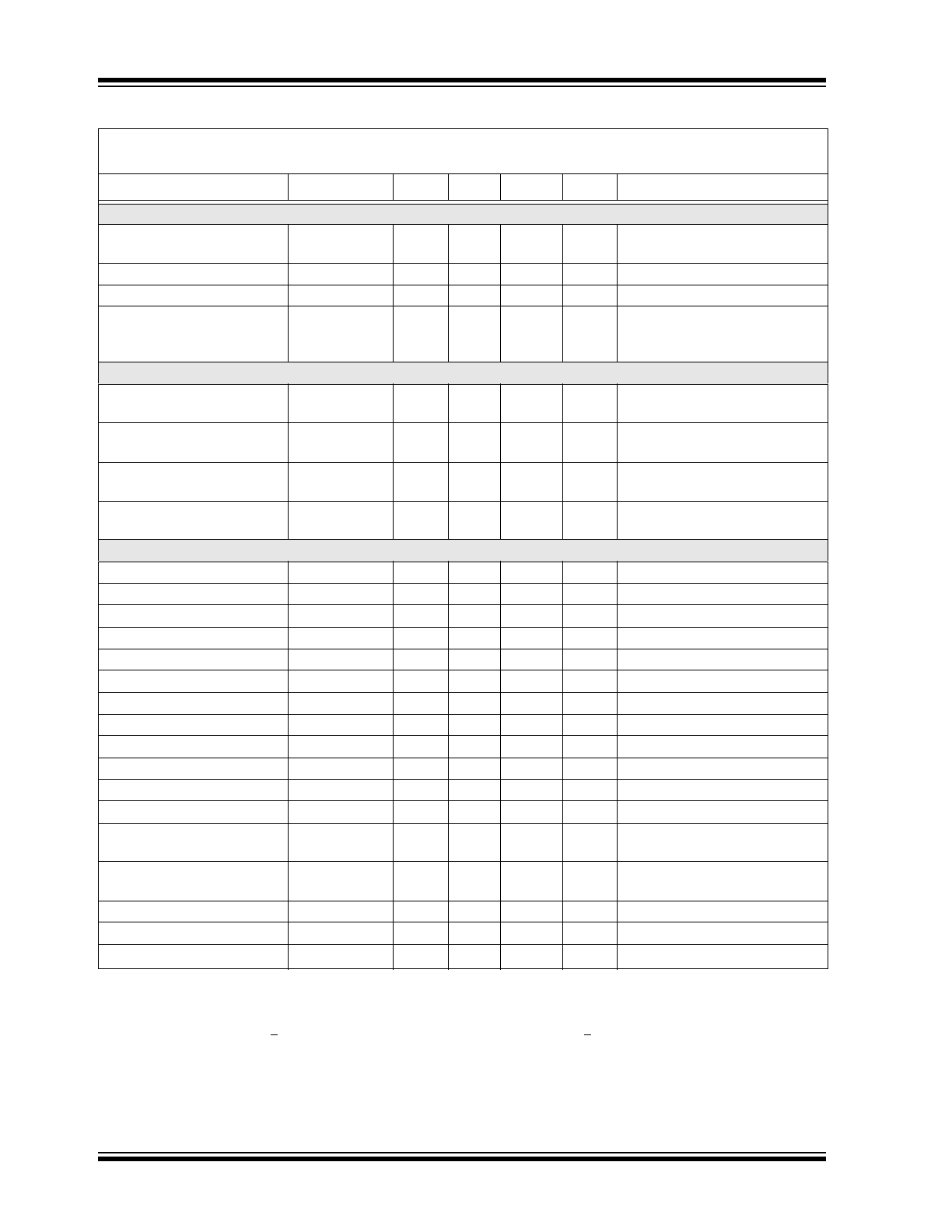
TABLE 1-1:
ELECTRICAL SPECIFICATIONS (CONTINUED)
Electrical Characteristics: Unless otherwise specified, V
DD
= 4.5V to 5.5V, V
S
= 2.9V to 5.5V,
V
PULLUP
= 3V to 5.5V, T
A
= –40°C to 105°C. All typical values at V
DD
= V
S
= 5V, T
A
= 27°C.
Characteristic
Symbol
Min.
Typ.
Max.
Unit
Conditions
Note 1:
This parameter is characterized, not 100% tested.
2:
This parameter is ensured by design and not 100% tested.
3:
The current measurement full scale range maximum value is 3.4A. However, the UCS2114 cannot report values above
I
LIM
(if I
BUS_R2MIN
I
LIM
) or above I
BUS_R2MIN
(if I
BUS_R2MIN
> I
LIM
and I
LIM
1.6A).
2017 Microchip Technology Inc.
DS20005743A-page 5
UCS2114
Port Power Switch
Port Power Switch - DC Parameter
Overvoltage Lockout
V
S_OV
—
6
—
V
Note 2
V
S
Low Threshold
V
S_UVLO
—
2.5
—
V
Note 2
V
S
Low Hysteresis
V
S_UVLO_HYST
—
100
—
mV
Note 2
On Resistance
R
ON_PSW
—
18
30
m
4.75V < V
S
< 5.25V
V
S
Leakage Current
I
LEAK_VS
—
—
5
µA
Sleep state into V
S
pin on one
channel (
Note 1
)
Back-Voltage Protection
Threshold
V
BV_TH
—
150
—
mV
V
BUS
> V
S
V
S
> V
S_UVLO
Leakage Current
I
LKG_1
—
0
3
µA
V
DD
< V
DD_TH
,
Leakage current from V
BUS
pins
to the V
DD
and the V
S
pins
(
Note 1
)
I
LKG_2
—
0
2
µA
V
DD
> V
DD_TH
,
Leakage current from V
BUS
pins
to the V
S
pins, when the power
switch is open
Selectable Current Limits
I
LIM1
—
530
—
mA
I
LIM
Resistor = 0 or 47 k
(530 mA setting)
I
LIM2
—
960
—
mA
I
LIM
Resistor = 10 k
or 56 k
(960 mA setting)
I
LIM3
—
1070
—
mA
I
LIM
Resistor = 12 k
or 68 k
(1070 mA setting)
I
LIM4
—
1280
—
mA
I
LIM
Resistor = 15 k
or 82 k
(1280 mA setting)
I
LIM5
—
1600
—
mA
I
LIM
Resistor = 18 k
or 100 k
(1600 mA setting)
I
LIM6
—
2130
—
mA
I
LIM
Resistor = 22 k
or 120 k
(2130 mA setting)
I
LIM7
2500
2670
2900
mA
I
LIM
Resistor = 27 k
or 150 k
(2670 mA setting)
I
LIM8
3000
3200
3400
mA
I
LIM
Resistor = 33 k
or V
DD
(3200 mA setting)
Pin Wake Time
t
PIN_WAKE
—
3
—
ms
SMBus Wake Time
t
SMB_WAKE
—
4
—
ms
Idle Sleep Time
t
IDLE_SLEEP
—
200
—
ms
First Thermal Shutdown
Stage Threshold
T
TSD_LOW
—
120
—
°C
Die Temperature at which the
power switch will open if it is in
Constant Current mode
TABLE 1-1:
ELECTRICAL SPECIFICATIONS (CONTINUED)
Electrical Characteristics: Unless otherwise specified, V
DD
= 4.5V to 5.5V, V
S
= 2.9V to 5.5V,
V
PULLUP
= 3V to 5.5V, T
A
= –40°C to 105°C. All typical values at V
DD
= V
S
= 5V, T
A
= 27°C.
Characteristic
Symbol
Min.
Typ.
Max.
Unit
Conditions
Note 1:
This parameter is characterized, not 100% tested.
2:
This parameter is ensured by design and not 100% tested.
3:
The current measurement full scale range maximum value is 3.4A. However, the UCS2114 cannot report values above
I
LIM
(if I
BUS_R2MIN
I
LIM
) or above I
BUS_R2MIN
(if I
BUS_R2MIN
> I
LIM
and I
LIM
1.6A).
UCS2114
DS20005743A-page 6
2017 Microchip Technology Inc.
First Thermal Shutdown
Stage Hysteresis
T
TSD_LOW_HYST
—
10
—
°C
Hysteresis for T
TSD_LOW
func-
tionality. Temperature must drop
by this value before any of the
power switches can be closed.
Second Thermal Shutdown
Stage Threshold
T
TSD_HIGH
—
135
—
°C
Die Temperature at which both
power switches will open
Second Thermal Shutdown
Stage Hysteresis
T
TSD_HIGH_HYST
—
25
—
°C
Hysteresis for T
TSD_HIGH
functionality. Temperature must
drop by this value before any of
the power switches can be
closed.
Auto-Recovery Test Current
I
TEST
—
190
—
mA
Portable device attached,
V
BUS
= 0 V, Die temp < T
TSD
Auto-Recovery Test Voltage
V
TEST
—
750
—
mV
Portable device attached,
V
BUS
= 0 V before application,
Die temp < T
TSD
Programmable, 250-1000 mV,
default listed
Discharge Impedance
R
DISCHARGE
—
100
—
Port Power Switch - AC Parameters
Turn-on Delay
t
ON_PSW
—
0.9
—
ms
PWR_EN active toggle to
switch on time, V
BUS
discharge
not active
Turn-off Time
t
OFF_PSW_INA
—
0.75
—
ms
PWR_EN inactive toggle to
switch off time
C
BUS
= 120 µF
Turn-off Time
t
OFF_PSW_ERR
—
1
—
ms
Overcurrent Error, V
BUS
Min
Error, or Discharge Error to
switch off
C
BUS
= 120 µF
Turn-off Time
t
OFF_PSW_ERR1
—
100
—
ns
TSD or Back-drive Error to
switch off
C
BUS
= 120 µF
V
BUS
Output Rise Time
t
R_BUS
—
1.1
—
ms
Measured from 10% to 90% of
V
BUS
, C
LOAD
= 220 µF
I
LIM
= 1.0A
Soft Turn-On Rate
I
BUS
/
t
—
100
—
mA/µs
Temperature Update Time
t
DC_TEMP
—
200
—
ms
Short-Circuit Response Time
t
SHORT_LIM
—
1.5
—
µs
Time from detection of short to
current limit applied.
No C
BUS
applied
Short-Circuit Detection Time
t
SHORT
—
6
—
ms
Time from detection of short to
port power switch disconnect
and ALERT# pin assertion
TABLE 1-1:
ELECTRICAL SPECIFICATIONS (CONTINUED)
Electrical Characteristics: Unless otherwise specified, V
DD
= 4.5V to 5.5V, V
S
= 2.9V to 5.5V,
V
PULLUP
= 3V to 5.5V, T
A
= –40°C to 105°C. All typical values at V
DD
= V
S
= 5V, T
A
= 27°C.
Characteristic
Symbol
Min.
Typ.
Max.
Unit
Conditions
Note 1:
This parameter is characterized, not 100% tested.
2:
This parameter is ensured by design and not 100% tested.
3:
The current measurement full scale range maximum value is 3.4A. However, the UCS2114 cannot report values above
I
LIM
(if I
BUS_R2MIN
I
LIM
) or above I
BUS_R2MIN
(if I
BUS_R2MIN
> I
LIM
and I
LIM
1.6A).
2017 Microchip Technology Inc.
DS20005743A-page 7
UCS2114
Latched Mode Cycle Time
t
UL
—
7
—
ms
From PWR_EN edge transition
from inactive to active to begin
error recovery.
Auto-Recovery Mode Cycle
Time
t
CYCLE
—
25
—
ms
Time delay before error
condition check.
Programmable 15-50 ms,
default listed.
Auto-Recovery Delay
t
TST
—
20
—
ms
Portable device attached, V
BUS
must be > V
TEST
after this time.
Programmable 10-25 ms,
default listed.
Discharge Time
t
DISCHARGE
—
200
—
ms
Amount of time discharge
resistor applied.
Programmable 100-400 ms,
default listed.
Port Power Switch Operation with Trip Mode Current Limiting
Region 2 Current
Keep-Out
I
BUS_R2MIN_1
—
—
0.1
A
Note 2
Minimum V
BUS
Allowed at Output
V
BUS_MIN_1
2.0
—
—
V
Note 2
Port Power Switch Operation with Constant Current Limiting (Variable Slope)
Region 2 Current
Keep-Out
I
BUS_R2MIN
—
—
2.13
A
Note 2
Minimum V
BUS
Allowed at Output
V
BUS_MIN
2.0
—
—
V
Note 2
Current Measurement - DC
Current Measurement Range
I
BUS_M
0
—
3400
mA
Range (
Note 2
and
Note 3
)
Reported Current
Measurement Resolution
I
BUS_M
—
13.3
—
mA
1 LSB
Current Measurement
Accuracy
—
±2
—
%
200 mA < I
BUS
< I
LIM
—
±2
—
LSB
I
BUS
< 200 mA
Current Measurement - AC
Sampling Rate
—
—
1.1
—
ms
Note 2
Conversion Time
Both Channels
t
CONV
—
2.2
—
ms
All registers updated in digital
(
Note 2
)
Charge Rationing - DC
Accumulated Current
Measurement Accuracy
—
—
±4.5
—
%
Charge Rationing - AC
Current Measurement
Update Time
t
PCYCLE
—
1
—
s
TABLE 1-1:
ELECTRICAL SPECIFICATIONS (CONTINUED)
Electrical Characteristics: Unless otherwise specified, V
DD
= 4.5V to 5.5V, V
S
= 2.9V to 5.5V,
V
PULLUP
= 3V to 5.5V, T
A
= –40°C to 105°C. All typical values at V
DD
= V
S
= 5V, T
A
= 27°C.
Characteristic
Symbol
Min.
Typ.
Max.
Unit
Conditions
Note 1:
This parameter is characterized, not 100% tested.
2:
This parameter is ensured by design and not 100% tested.
3:
The current measurement full scale range maximum value is 3.4A. However, the UCS2114 cannot report values above
I
LIM
(if I
BUS_R2MIN
I
LIM
) or above I
BUS_R2MIN
(if I
BUS_R2MIN
> I
LIM
and I
LIM
1.6A).
UCS2114
DS20005743A-page 8
2017 Microchip Technology Inc.
FIGURE 1-1:
SMBus Timing.
SMDATA
SMCLK
T
BUF
P
S
S - Start Condition
P - Stop Condition
P
S
T
HIGH
T
LOW
T
HD:STA
T
SU:STO
T
HD:STA
T
HD:DAT
T
SU:DAT
T
SU:STA
T
FALL
T
RISE
TABLE 1-2:
TEMPERATURE SPECIFICATIONS
Parameters
Sym.
Min.
Typ.
Max.
Units
Conditions
Temperature Ranges
Operating Temperature Range
T
A
-40
—
+105
°C
Operating Junction Temperature
T
J
-40
—
+125
°C
Storage Temperature Range
T
A
-55
—
+150
°C
Thermal Package Resistances
3x3 mm 20-pin VQFN
θ
JA
—
48
—
°C/W
Typical 4-layer board
with interconnecting
vias, recommended
land pattern from this
document.

2017 Microchip Technology Inc.
DS20005743A-page 9
UCS2114
1.1
ESD and Transient Performance
1.1.1
HUMAN BODY MODEL (HBM)
PERFORMANCE
HBM testing verifies the ability to withstand ESD
strikes, like those that occur during handling and
manufacturing, and is done without power applied to
the IC. To pass the test, the device must have no
change in operation or performance due to the event.
1.1.2
CHARGED DEVICE MODEL (CDM)
PERFORMANCE
CDM testing verifies the ability to withstand ESD
strikes, like those that occur during handling and
assembly, with pick-and-place-style machinery and is
done without power applied to the IC. To pass the test,
the device must have no change in operation or
performance due to the event.
TABLE 1-3:
ESD RATINGS
ESD Specification
Rating or Value
Human Body Model (JEDEC JESD22-A114) - All pins
8 kV
Charged Device Model (JEDEC JESD22-C101) - All pins
500V

UCS2114
DS20005743A-page 10
2017 Microchip Technology Inc.
NOTES: