

2014-2015 Microchip Technology Inc.
DS20005346B-page 1
UCS1003-1/2/3
Features
• Port Power Switch with Two Current Limit Behaviors:
- 2.9V to 5.5V source voltage range
- Up to 3.0A current (2.85A typical) with 55 m
on resistance
- Overcurrent trip or Constant-Current Limiting
- Soft turn-on circuitry
- Selectable current limit
- UCS1003-1 has programmable current limit via
the SMBus 2.0/I
2
C protocol
- Dynamic thermal management
- Undervoltage Lockout (UVLO) and Overvoltage
Lockout (OVLO)
- Backdrive, back-voltage protection
- Latch or auto-recovery (low test current) Fault handling
- Selectable active-high or active-low power
switch enable
- BC1.2 V
BUS
discharge port renegotiation function
• Selectable/Automatic Cycling of Universal Serial Bus
(USB) Data Line Charger Emulation Profiles:
- USB-IF BC1.2 Charging Downstream Port (CDP)
and Dedicated Charging Port (DCP) modes,
Chinese Telecommunications Industry Standard
YD/T 1591-2009 and most Apple
®
Inc.,
Samsung and RIM
®
protocols standard
- UCS1003-1 supports other charger emulation
profiles as defined via the SMBus 2.0/I
2
C protocol
- Supports 12W charging emulation
- USB 2.0 compliant high-speed data switch (in
Data Pass-Through, SDP and CDP modes)
- Nine preloaded charger emulation profiles for
maximum compatibility coverage of the
peripheral devices
- UCS1003-1 has one custom programmable
charger emulation profile for portable device
support for fully host-controlled charger emulation
• Supports Active Cables
• UCS1003-1 Supports Self-Contained Current Monitoring
and Rationing for Power Allocation Applications
• UCS1003-1 and UCS1003-3 have Low-Power
Attach Detection and Open-Drain (A_DET#) Pin
• UCS1003-2 has Charging Active (CHRG#)
Open-Drain Pin
• Ultra Low-Power Sleep State
• Optional Split Supply Support for V
S
and V
DD
for
Low Power in System Standby States
• Wake on Attach USB (UCS1003-1 and UCS1003-3)
• UCS1003-1 Supports SMBus 2.0/I
2
C Communications:
- Supports block write and read
- Multiple SMBus addresses
• Wide Operating Temperature Range: -40°C to +85°C
• IEC61000-4-2 8/15 kV Electrostatic Discharge (ESD)
Immunity
• UL Recognized and EN/IEC 60950-1 (CB) Certified
Description
The UCS1003-1/2/3 family of devices provides a USB
port power switch for precise control of up to 3.0A
continuous current (2.85A typical) with Overcurrent
Limit (OCL), dynamic thermal management, latch or
auto-recovery (low test current) Fault handling, select-
able active-high or active-low enable, Undervoltage
and Overvoltage Lockout, backdrive protection and
back-voltage protection.
Split supply support for V
S
and V
DD
is an option for low
power in system standby states. This gives battery-
operated applications (such as on-board computers) the
ability to detect attachments from a Sleep or OFF state.
After the Attach Detection is flagged, the system can
decide to wake-up and/or provide charging.
In addition to Power Switching and Current-Limiting
modes, the UCS1003-1/2/3 will automatically charge a
wide variety of portable devices, including USB-IF
BC1.2, YD/T-1591 (2009), most Apple Inc., Samsung,
RIM and many others. Nine preloaded charger emula-
tion profiles maximize the compatibility coverage of the
peripheral devices. Additionally, a customizable
charger emulation profile is available in UCS1003-1 to
accommodate unique existing and future portable
device handshaking/signature requirements.
The UCS1003-1 also provides current monitoring to
allow intelligent management of system power and
charge rationing for controlled delivery of current, regard-
less of the host power state. This is especially important
for battery-operated applications that want to provide
power and do not want to drain the battery excessively.
The UCS1003-1/2/3 family is available in a
4 mm x 4 mm 20-pin QFN package.
Applications
• Notebook and Netbook Computers
• Tablets and E-Book Readers
• Desktops and Monitors
• Docking Stations and Printers
• AC-DC Wall Adapters
USB Port Power Controller with Charger Emulation
UCS1003-1/2/3
DS20005346B-page 2
2014-2015 Microchip Technology Inc.
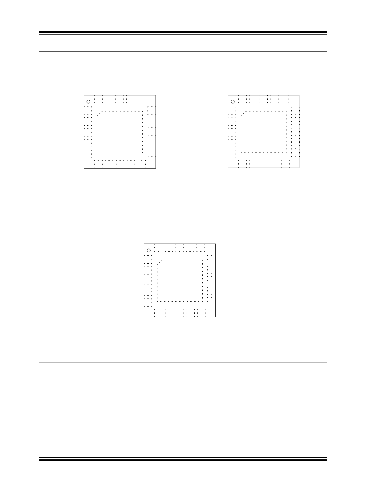
Package Type
2
1
3
4
5
15
D
MO
UT
V
BUS1
V
BUS2
M1
D
MIN
D
PIN
SE
L
ALERT#
V
S1
V
S2
V
DD
SMCLK/S0
GND
EM
_EN
A_D
E
T
#
D
PO
UT
M2
EP
20 19 18 17
14
13
12
11
6
7
8
9
21
10
15
16
COMM_SEL/I
LIM
PWR
_
E
N
SMDATA/LATCH
*
Includes Exposed Thermal Pad (EP); see
Table 3-1
.
D
MO
UT
2
V
BUS1
V
BUS2
M1
D
MIN
D
PIN
SEL
ALERT#
V
S1
V
S2
V
DD
S0
GND
EM
_
E
N
CH
RG#
D
PO
UT
M2
EP
20
1
19 18 17
3
4
14
13
12
11
6
7
8
9
21
5
10
16
I
LIM
PWR
_
E
N
LATCH
UCS1003-1
4x4 QFN*
UCS1003-2
4x4 QFN*
D
MO
UT
2
V
BUS1
V
BUS2
M1
D
MIN
D
PIN
SE
L
ALERT#
V
S1
V
S2
V
DD
S0
GND
EM
_EN
A_D
E
T#
D
PO
UT
M2
EP
20
1
19 18 17
3
4
14
13
12
11
6
7
8
9
21
5
10
15
16
I
LIM
PW
R
_
E
N
LATCH
UCS1003-3
4x4 QFN*
2014-2015 Microchip Technology Inc.
DS20005346B-page 3
UCS1003-1/2/3
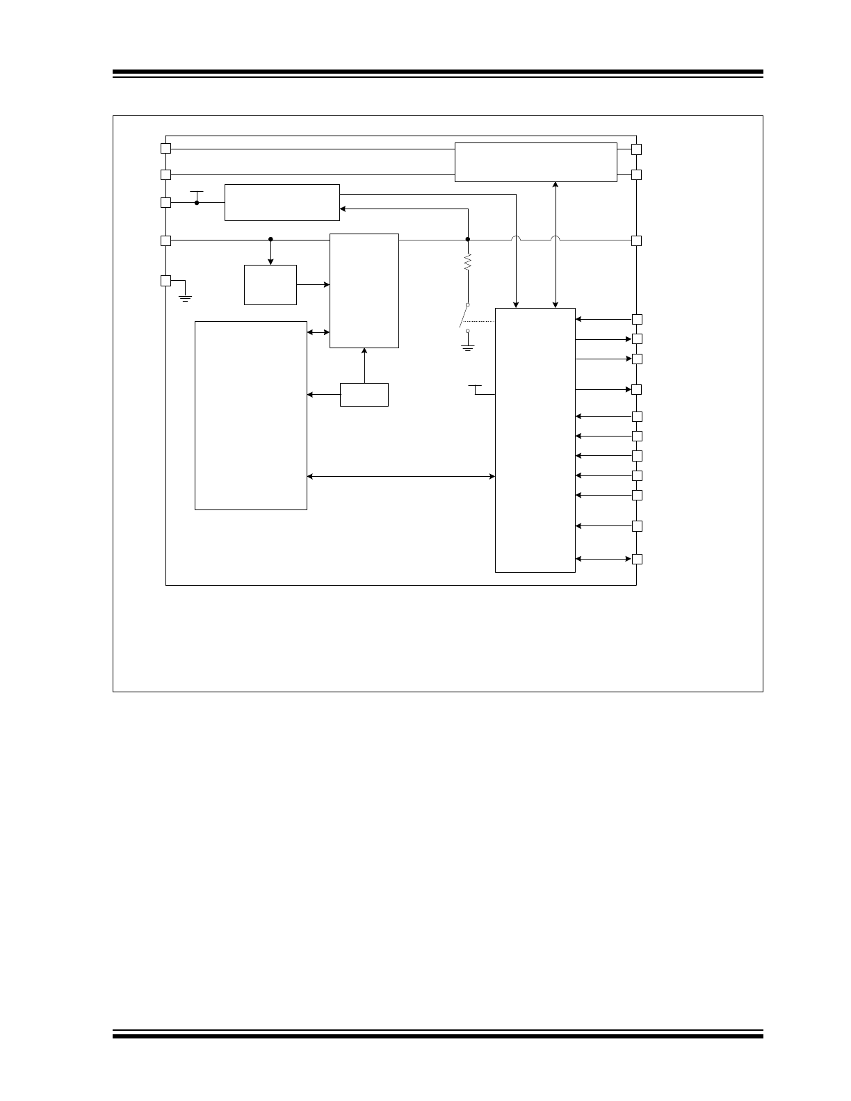
Block Diagram
Note 1:
Available for UCS1003-1 only.
2:
Available for UCS1003-2 only.
3:
Available for UCS1003-3 only.
Charger Control,
Measurement,
OCL
Interface,
Logic
SMCLK
(1)
/S0
SMDATA
(1)
/LATCH
A_DET#
(1,3)
ALERT#
Power
Switch
Temp
PWR_EN
D
POUT
D
MOUT
D
PIN
V
DD
V
S
V
BUS
D
MIN
GND
USB 2.0 HS Data Switch &
Charger Emulator
COMM_SEL
(1)
/I
LIM
Attach Detector
M1
M2
SEL
EM_EN
V
DD
V
DD
UVLO,
OVLO
CHRG#
(2)

UCS1003-1/2/3
DS20005346B-page 4
2014-2015 Microchip Technology Inc.
NOTES:
2014-2015 Microchip Technology Inc.
DS20005346B-page 5
UCS1003-1/2/3
1.0
ELECTRICAL
CHARACTERISTICS
Absolute Maximum Ratings
†
Voltage on V
DD
, V
S
and V
BUS
Pins ....................................................................................................................-0.3 to 6V
Pull-up Voltage (V
PULLUP
) .................................................................................................................... -0.3 to V
DD
+ 0.3V
Data Switch Current (I
HSW_ON
), Switch On...........................................................................................................±50 mA
Port Power Switch Current .................................................................................................................... Internally Limited
Data Switch Pin Voltage To Ground (D
POUT
, D
PIN
, D
MOUT
, D
MIN
); (V
DD
powered or unpowered)....... -0.3 to V
DD
+ 0.3V
Differential Voltage Across Open Data Switch (D
POUT
– D
PIN
, D
MOUT
– D
MIN
, D
PIN
– D
POUT
, D
MIN
– D
MOUT
) .........V
DD
Voltage on any Other Pin to Ground ................................................................................................... -0.3 to V
DD
+ 0.3V
Current on any Other Pin ......................................................................................................................................±10 mA
Package Power Dissipation ...............................................................................................................................
Table 1-1
Operating Ambient Temperature Range .....................................................................................................-40 to +125°C
Storage Temperature Range.......................................................................................................................-55 to +150°C
† Notice:
Stresses above those listed under “Maximum Ratings” may cause permanent damage to the device. This
is a stress rating only and functional operation of the device at those or any other conditions above those indicated in
the operational listings of this specification is not implied. Exposure to maximum rating conditions for extended periods
may affect device reliability.
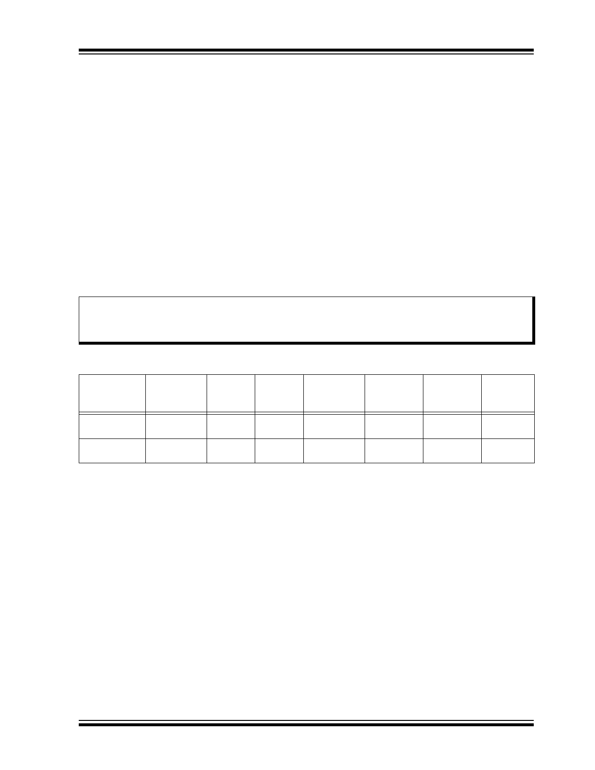
TABLE 1-1:
POWER DISSIPATION SUMMARY
Board
Package
JC
JA
Derating
Factor Above
+25°C
T
A
< +25°C
Power
Rating
T
A
< +70°C
Power
Rating
T
A
< +85°C
Power
Rating
High K
(see
Note 1
)
20-pin QFN
4 x 4 mm
6°C/W
41°C/W
24.4 mW°/C
2193 mW
1095 mW
729 mW
Low K
(see
Note 1
)
20-pin QFN
4 x 4 mm
6°C/W
60°C/W
16.67 mW°/C
1498 mW
748 mW
498 mW
Note 1:
Junction to ambient (
JA
) is dependent on the design of the thermal vias. A High K board uses a thermal
via design with a thermal landing soldered to the PCB ground plane, with 0.3 mm (12 mil) diameter vias in
a 3x3 matrix (9 total) at 0.5 mm (20 mil) pitch. The board is multilayer with 1-ounce internal power and
ground planes and 2-ounce copper traces on top and bottom. A Low K board is a two-layer board without
thermal via design, with 2-ounce copper traces on the top and bottom.
UCS1003-1/2/3
DS20005346B-page 6
2014-2015 Microchip Technology Inc.
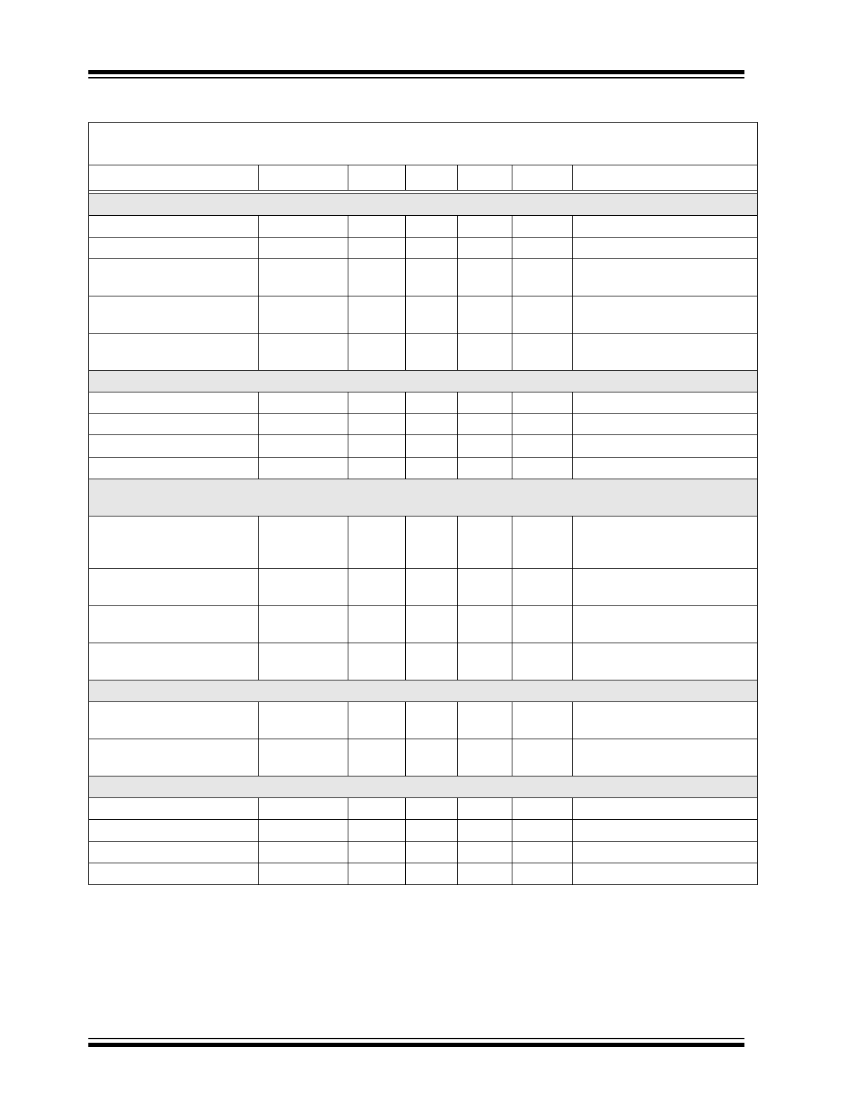
TABLE 1-2:
ELECTRICAL CHARACTERISTICS
Electrical Characteristics:
Unless otherwise specified, V
DD
= 4.5V to 5.5V, V
S
= 2.9V to 5.5V, V
PULLUP
= 3V to 5.5V,
T
A
= -40°C to +85°C; all Typical values at V
DD
= V
S
= 5V, T
A
= +27°C.
Characteristic
Sym.
Min.
Typ.
Max.
Unit
Conditions
Power Supply
Supply Voltage
V
DD
4.5
5
5.5
V
(
Note 1
)
Source Voltage
V
S
2.9
5
5.5
V
(
Note 1
)
Supply Current in Active
(I
DD_ACTIVE
+ I
VS_ACT
)
I
ACTIVE
—
650
750
µA
Average current, I
BUS
= 0 mA
Supply Current in Sleep
(I
DD_SLEEP
+ I
VS_SLEEP
)
I
SLEEP
—
5
15
µA
Average current,
V
PULLUP
V
DD
Supply Current in Detect
(I
DD_DETECT
+ I
VS_DETECT
)
I
DETECT
—
185
—
µA
Average current,
no portable device attached
Power-on Reset
V
S
Low Threshold
V
S_UVLO
—
2.5
—
V
V
S
voltage increasing
V
S
Low Hysteresis
V
S_UVLO_HYST
—
100
—
mV
V
S
voltage decreasing
V
DD
Low Threshold
V
DD_TH
—
4
—
V
V
DD
voltage increasing
V
DD
Low Hysteresis
V
DD_TH_HYST
—
500
—
mV
V
DD
voltage decreasing
I/O Pins – SMCLK (UCS1003-1), SMDATA (UCS1003-1), EM_EN, M1, M2, PWR_EN, S0, LATCH, ALERT#, A_DET#
(UCS1003-1 and UCS1003-3), CHRG# (UCS1003-2) – DC Parameters
Output Low Voltage
V
OL
—
—
0.4
V
I
SINK_IO
= 8 mA,
SMDATA, ALERT#,
A_DET#, CHRG#
Input High Voltage
V
IH
2.0
—
—
V
PWR_EN, EM_EN, M1, M2,
LATCH, S0, SMDATA, SMCLK
Input Low Voltage
V
IL
—
—
0.8
V
PWR_EN, EM_EN, M1, M2,
LATCH, S0, SMDATA, SMCLK
Leakage Current
I
LEAK
—
—
±5
µA
Powered or unpowered,
V
PULLUP
V
DD
Interrupt Pins – AC Parameters
ALERT#, A_DET# Pins
Blanking Time
t
BLANK
—
25
—
ms
ALERT# Pin
Interrupt Masking Time
t
MASK
—
5
—
ms
SMBus/I
2
C Timing (UCS1003-1 only)
Input Capacitance
C
IN
—
5
—
pF
Clock Frequency
f
SMB
10
—
400
kHz
Spike Suppression
t
SP
—
50
ns
(
Note 2
)
Bus Free Time Stop to Start
t
BUF
1.3
—
—
µs
Note 1:
For split supply systems using the Attach Detection feature, V
S
must not exceed V
DD
+ 150 mV.
2:
This parameter is ensured by design and not 100% tested.
3:
This parameter is characterized, but not 100% production tested.
4:
The current measurement full-scale range maximum value is 3.0A. However, the UCS1003-1 cannot report
values above I
LIM
(if I
BUS_R2MIN
I
LIM
) or above I
BUS_R2MIN
(if I
BUS_R2MIN
> I
LIM
and I
LIM
1.68A).
5:
The Min and Max values represent the boundaries of a programmable range for UCS1003-1 only. Each value
in the range is typical.
2014-2015 Microchip Technology Inc.
DS20005346B-page 7
UCS1003-1/2/3
Start Setup Time
t
SU:STA
0.6
—
—
µs
Start Hold Time
t
HD:STA
0.6
—
—
µs
Stop Setup Time
t
SU:STO
0.6
—
—
µs
Data Hold Time
t
HD:DAT
0
—
—
µs
When transmitting to the master
Data Hold Time
t
HD:DAT
0.3
—
—
µs
When receiving from the master
Data Setup Time
t
SU:DAT
0.6
—
—
µs
Clock Low Period
t
LOW
1.3
—
—
µs
Clock High Period
t
HIGH
0.6
—
—
µs
Clock/Data Fall Time
t
FALL
—
—
300
ns
Min = 20 + 0.1 C
LOAD
ns (
Note 3
)
Clock/Data Rise Time
t
RISE
—
—
300
ns
Min = 20 + 0.1 C
LOAD
ns (
Note 3
)
Capacitive Load
C
LOAD
—
—
400
pF
Per bus line (
Note 2
)
Time-out
t
TIMEOUT
25
—
35
ms
Disabled by default (
Note 2
)
Idle Reset
t
IDLE_RESET
350
—
—
µs
Disabled by default (
Note 2
)
High-Speed Data Switch
High-Speed Data Switch – DC Parameters
Switch Leakage Current
I
HSW_OFF
—
±0.5
—
µA
Switch open – D
PIN
to D
POUT
,
D
MIN
to D
MOUT
or all four pins to
ground; V
DD
V
S
Charger Resistance
R
CHG
—
2
—
M
D
POUT
or D
MOUT
to V
BUS,
or
ground (see
Figure 1-2
),
BC1.2 DCP charger
emulation is active
On Resistance
R
ON_HSW
—
2
—
Switch closed, V
DD
= 5V
Test Current = 8 mA,
Test Voltage = 0.4V
(see
Figure 1-2
)
On Resistance
R
ON_HSW_1
—
5
—
Switch closed, V
DD
= 5V,
Test Current = 8 mA,
Test Voltage = 3.0V
(see
Figure 1-2
)
Delta-On Resistance
R
ON_HSW
—
±0.3
—
Switch closed, V
DD
= 5V,
I
TST
= 8 mA, V
TST
= 0 to 1.5V
(see
Figure 1-2
)
High-Speed Data Switch – AC Parameters
D
P
, D
M
Capacitance to Ground
C
HSW_ON
—
4
—
pF
Switch closed, V
DD
= 5V
D
P
, D
M
Capacitance to Ground
C
HSW_OFF
—
2
—
pF
Switch open, V
DD
= 5V
TABLE 1-2:
ELECTRICAL CHARACTERISTICS (CONTINUED)
Electrical Characteristics:
Unless otherwise specified, V
DD
= 4.5V to 5.5V, V
S
= 2.9V to 5.5V, V
PULLUP
= 3V to 5.5V,
T
A
= -40°C to +85°C; all Typical values at V
DD
= V
S
= 5V, T
A
= +27°C.
Characteristic
Sym.
Min.
Typ.
Max.
Unit
Conditions
Note 1:
For split supply systems using the Attach Detection feature, V
S
must not exceed V
DD
+ 150 mV.
2:
This parameter is ensured by design and not 100% tested.
3:
This parameter is characterized, but not 100% production tested.
4:
The current measurement full-scale range maximum value is 3.0A. However, the UCS1003-1 cannot report
values above I
LIM
(if I
BUS_R2MIN
I
LIM
) or above I
BUS_R2MIN
(if I
BUS_R2MIN
> I
LIM
and I
LIM
1.68A).
5:
The Min and Max values represent the boundaries of a programmable range for UCS1003-1 only. Each value
in the range is typical.
UCS1003-1/2/3
DS20005346B-page 8
2014-2015 Microchip Technology Inc.
Turn-Off Time
t
HSW_OFF
—
400
—
µs
Time from state control (EM_EN,
M1, M2) switch on to switch off,
R
TERM
= 50
, C
LOAD
= 5 pF
Turn-On Time
t
HSW_ON
—
400
—
µs
Time from state control (EM_EN,
M1, M2) switch off to switch on,
R
TERM
= 50
, C
LOAD
= 5 pF
Propagation Delay
t
PD
—
0.25
—
ns
R
TERM
= 50
, C
LOAD
= 5 pF
Propagation Delay Skew
t
PD
—
25
—
ps
R
TERM
= 50
, C
LOAD
= 5 pF
Rise/Fall Time
t
F/R
—
10
—
ns
R
TERM
= 50
, C
LOAD
= 5 pF
D
P
– D
M
Crosstalk
X
TALK
—
-40
—
dB
R
TERM
= 50
, C
LOAD
= 5 pF
Off Isolation
O
IRR
—
-30
—
dB
R
TERM
= 50
, C
LOAD
= 5 pF,
f = 240 MHz
-3 dB Bandwidth
BW
—
1100
—
MHz
R
TERM
= 50
, C
LOAD
= 5 pF,
V
DPOUT
= V
DMOUT
= 350 mV DC
Total Jitter
t
J
—
200
—
ps
R
TERM
= 50
, C
LOAD
= 5 pF,
Rise Time = Fall Time = 500 ps
at 480 Mbps (PRBS = 2
15
– 1)
Skew of Opposite Transitions
of the Same Output
t
SK(P)
—
20
—
ps
R
TERM
= 50
, C
LOAD
= 5 pF
Port Power Switch
Port Power Switch – DC Parameter
Overvoltage Lockout
V
S_OV
—
6
—
V
On Resistance
R
ON_PSW
—
55
—
m
4.75V < V
S
< 5.25V
V
S
Leakage Current
I
LEAK_VS
—
2.2
—
µA
Sleep state into V
S
pin
Back-Voltage Protection
Threshold
V
BV_TH
—
150
—
mV
V
BUS
> V
S
, V
S
> V
S_UVLO
Backdrive Current
I
BD_1
—
0
3
µA
V
DD
< V
DD_TH
,
Any powered power pin to any
unpowered power pin; current
out of unpowered pin (
Note 3
)
I
BD_2
—
0
2
µA
V
DD
< V
DD_TH
,
Any powered power pin to any
unpowered power pin, except
for V
DD
to V
BUS
in Detect power
state and V
S
to V
BUS
in Active
power state; current out of
unpowered pin (
Note 3
)
TABLE 1-2:
ELECTRICAL CHARACTERISTICS (CONTINUED)
Electrical Characteristics:
Unless otherwise specified, V
DD
= 4.5V to 5.5V, V
S
= 2.9V to 5.5V, V
PULLUP
= 3V to 5.5V,
T
A
= -40°C to +85°C; all Typical values at V
DD
= V
S
= 5V, T
A
= +27°C.
Characteristic
Sym.
Min.
Typ.
Max.
Unit
Conditions
Note 1:
For split supply systems using the Attach Detection feature, V
S
must not exceed V
DD
+ 150 mV.
2:
This parameter is ensured by design and not 100% tested.
3:
This parameter is characterized, but not 100% production tested.
4:
The current measurement full-scale range maximum value is 3.0A. However, the UCS1003-1 cannot report
values above I
LIM
(if I
BUS_R2MIN
I
LIM
) or above I
BUS_R2MIN
(if I
BUS_R2MIN
> I
LIM
and I
LIM
1.68A).
5:
The Min and Max values represent the boundaries of a programmable range for UCS1003-1 only. Each value
in the range is typical.
2014-2015 Microchip Technology Inc.
DS20005346B-page 9
UCS1003-1/2/3
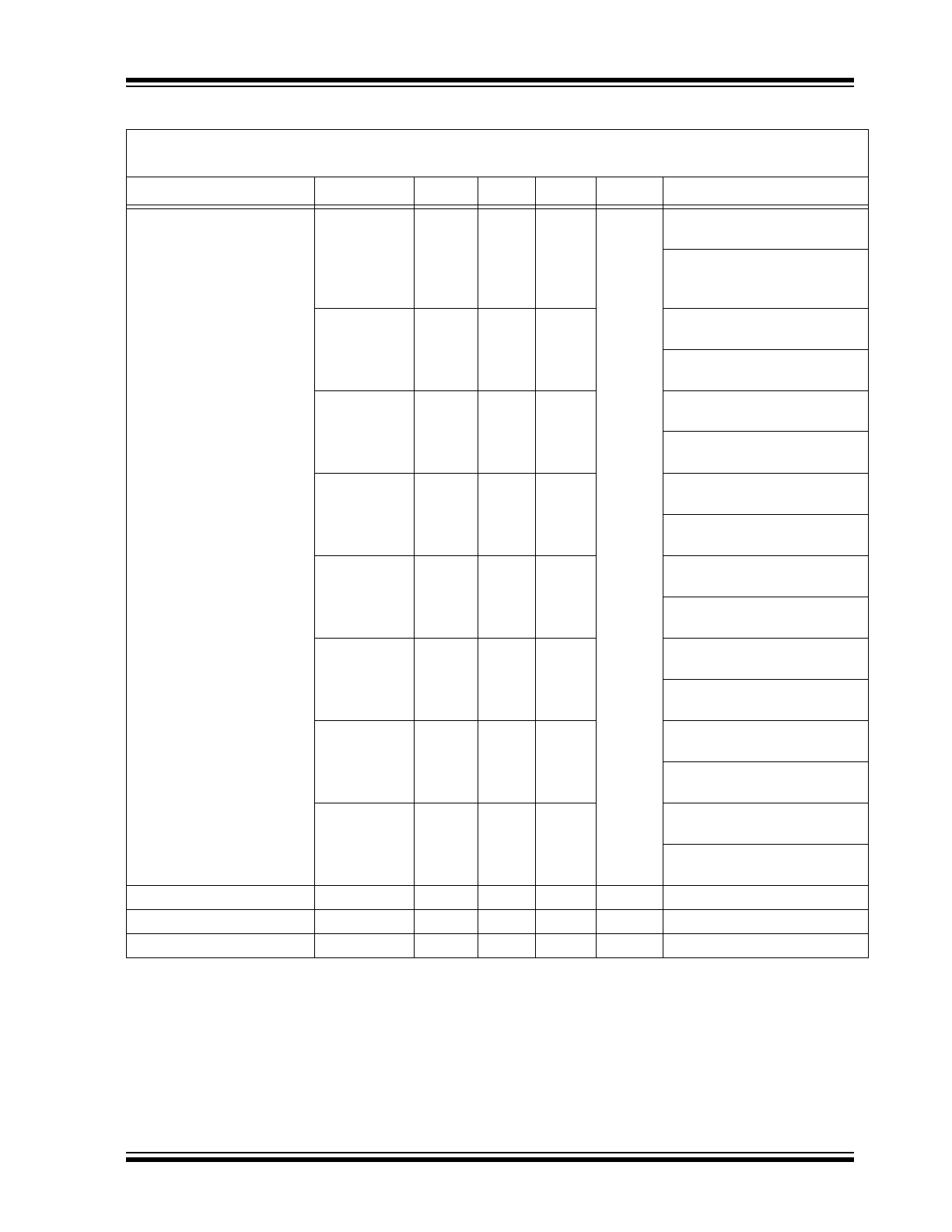
Selectable Current Limits
I
LIM1
—
570
—
mA
I
LIM
Resistor = 0 or 47 k
(UCS1003-1 only)
I
LIM
Resistor = 47 k
(UCS1003-2/3)
(minimum mA setting)
I
LIM2
—
1000
—
I
LIM
Resistor = 10 k
or 56 k
(UCS1003-1 only)
I
LIM
Resistor = 56 k
(UCS1003-2/3)
I
LIM3
—
1130
—
I
LIM
Resistor = 12 k
or 68 k
(UCS1003-1 only)
I
LIM
Resistor = 68 k
(UCS1003-2/3)
I
LIM4
—
1350
—
I
LIM
Resistor = 15 k
or 82 k
(UCS1003-1 only)
I
LIM
Resistor = 82 k
(UCS1003-2/3)
I
LIM5
—
1680
—
I
LIM
Resistor = 18 k
or 100 k
(UCS1003-1 only)
I
LIM
Resistor = 100 k
(UCS1003-2/3)
I
LIM6
—
2050
—
I
LIM
Resistor = 22 k
or 120 k
(UCS1003-1 only)
I
LIM
Resistor = 120 k
(UCS1003-2/3)
I
LIM7
—
2280
—
I
LIM
Resistor = 27 k
or 150 k
(UCS1003-1 only)
I
LIM
Resistor = 150 k
(UCS1003-2/3)
I
LIM8
2700
2850
3000
I
LIM
Resistor = 33 k
or V
DD
(UCS1003-1 only)
I
LIM
Resistor = V
DD
(UCS1003-2/3)
Pin Wake Time
t
PIN_WAKE
—
3
—
ms
SMBus Wake Time
t
SMB_WAKE
—
4
—
ms
(UCS1003-1 only)
Idle Sleep Time
t
IDLE_SLEEP
—
200
—
ms
(UCS1003-1 only)
TABLE 1-2:
ELECTRICAL CHARACTERISTICS (CONTINUED)
Electrical Characteristics:
Unless otherwise specified, V
DD
= 4.5V to 5.5V, V
S
= 2.9V to 5.5V, V
PULLUP
= 3V to 5.5V,
T
A
= -40°C to +85°C; all Typical values at V
DD
= V
S
= 5V, T
A
= +27°C.
Characteristic
Sym.
Min.
Typ.
Max.
Unit
Conditions
Note 1:
For split supply systems using the Attach Detection feature, V
S
must not exceed V
DD
+ 150 mV.
2:
This parameter is ensured by design and not 100% tested.
3:
This parameter is characterized, but not 100% production tested.
4:
The current measurement full-scale range maximum value is 3.0A. However, the UCS1003-1 cannot report
values above I
LIM
(if I
BUS_R2MIN
I
LIM
) or above I
BUS_R2MIN
(if I
BUS_R2MIN
> I
LIM
and I
LIM
1.68A).
5:
The Min and Max values represent the boundaries of a programmable range for UCS1003-1 only. Each value
in the range is typical.
UCS1003-1/2/3
DS20005346B-page 10
2014-2015 Microchip Technology Inc.
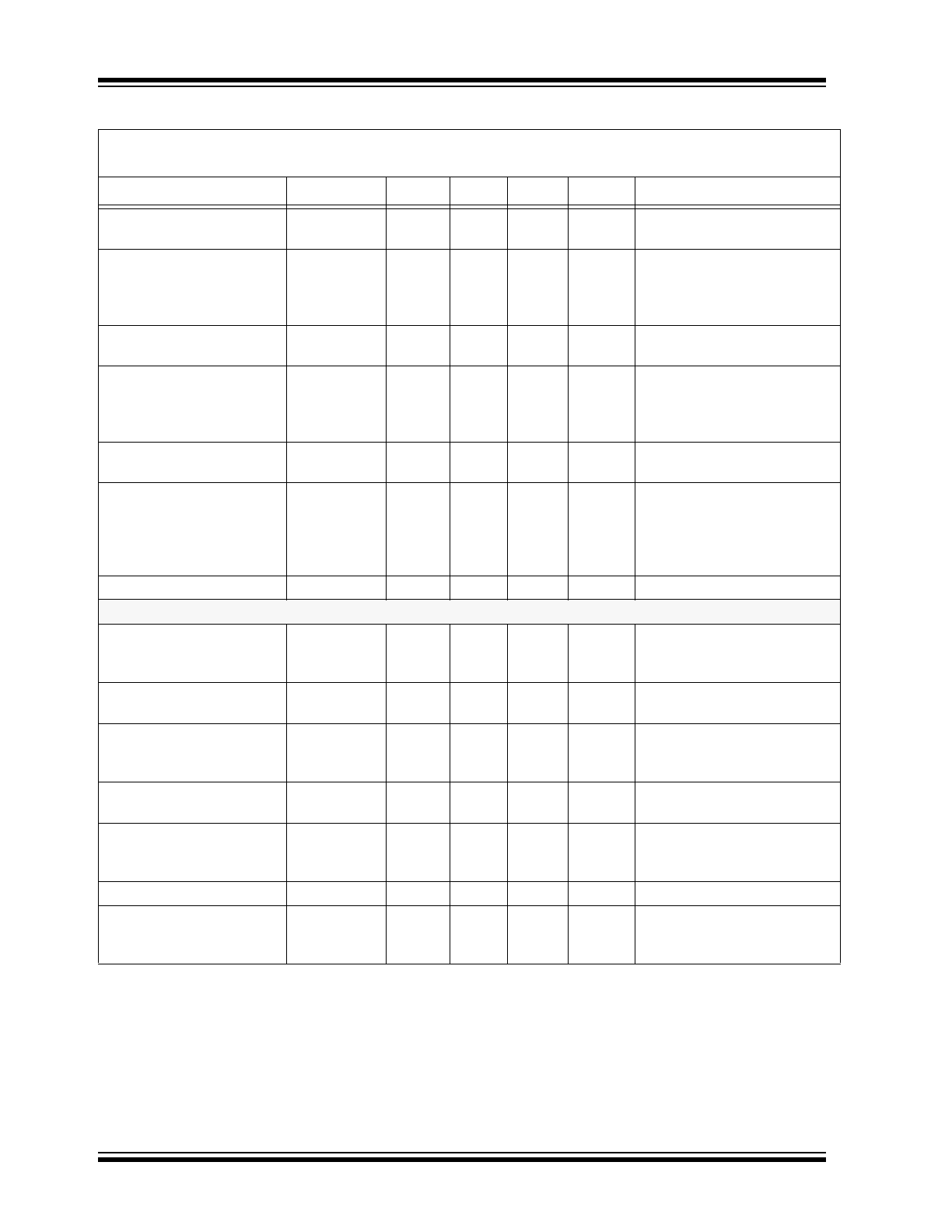
Thermal Regulation Limit
T
REG
—
110
—
°C
Die temperature at which
current limit will be reduced
Thermal Regulation
Hysteresis
T
REG_HYST
—
10
—
°C
Hysteresis for t
REG
functionality;
temperature must drop by this
value before I
LIM
value is
restored to normal operation
Thermal Shutdown
Threshold
T
TSD
—
135
—
°C
Die temperature at which port
power switch will turn off
Thermal Shutdown
Hysteresis
T
TSD_HYST
—
35
—
°C
After shutdown, due to T
TSD
being reached, die temperature
drop required before port power
switch can be turned on again
Auto-Recovery Test Current
I
TEST
—
190
—
mA
Portable device attached,
V
BUS
= 0V, Die Temp < T
TSD
Auto-Recovery Test Voltage
V
TEST
—
750
—
mV
Portable device attached,
V
BUS
= 0V before application,
Die Temp < T
TSD
programmable
(UCS1003-1 only)
,
250-1000 mV, default listed
Discharge Impedance
R
DISCHARGE
—
100
—
Port Power Switch – AC Parameters
Turn-On Delay
t
ON_PSW
—
0.75
—
ms
PWR_EN active toggle to switch
on time, V
BUS
discharge is not
active
Turn-Off Time
t
OFF_PSW_INA
—
0.75
—
ms
PWR_EN inactive toggle to
switch off time, C
BUS
= 120 μF
Turn-Off Time
t
OFF_PSW_ERR
—
1
—
ms
Overcurrent error, V
BUS
min
error or discharge error to
switch off, C
BUS
= 120 μF
Turn-Off Time
t
OFF_PSW_ERR
—
100
—
ns
TSD or backdrive error to switch
off, C
BUS
= 120 μF
V
BUS
Output Rise Time
t
R_BUS
—
1.1
—
ms
Measured from 10% to 90% of
V
BUS
, C
LOAD
= 220 μF,
I
LIM
= 1.0A
Soft Turn-on Rate
I
BUS
/
t
—
100
—
mA/µs
Temperature Update Time
t
DC_TEMP
—
200
—
ms
Programmable
(UCS1003-1 only)
200-1600 ms, default listed
TABLE 1-2:
ELECTRICAL CHARACTERISTICS (CONTINUED)
Electrical Characteristics:
Unless otherwise specified, V
DD
= 4.5V to 5.5V, V
S
= 2.9V to 5.5V, V
PULLUP
= 3V to 5.5V,
T
A
= -40°C to +85°C; all Typical values at V
DD
= V
S
= 5V, T
A
= +27°C.
Characteristic
Sym.
Min.
Typ.
Max.
Unit
Conditions
Note 1:
For split supply systems using the Attach Detection feature, V
S
must not exceed V
DD
+ 150 mV.
2:
This parameter is ensured by design and not 100% tested.
3:
This parameter is characterized, but not 100% production tested.
4:
The current measurement full-scale range maximum value is 3.0A. However, the UCS1003-1 cannot report
values above I
LIM
(if I
BUS_R2MIN
I
LIM
) or above I
BUS_R2MIN
(if I
BUS_R2MIN
> I
LIM
and I
LIM
1.68A).
5:
The Min and Max values represent the boundaries of a programmable range for UCS1003-1 only. Each value
in the range is typical.