
© 2011 Microchip Technology Inc.
DS22192D-page 1
MCP3901
Features
• Two Synchronous Sampling 16/24-bit Resolution
Delta-Sigma A/D Converters with Proprietary
Multi-Bit Architecture
• 91 dB SINAD, -104 dBc Total Harmonic Distortion
(THD) (up to 35
th
harmonic), 109 dB Spurious-free
Dynamic Range (SFDR) for Each Channel
• Programmable Data Rate up to 64 ksps
• Ultra Low-Power Shutdown mode with <2 µA
• -133 dB Crosstalk Between the Two Channels
• Low Drift Internal Voltage Reference: 12 ppm/°C
• Differential Voltage Reference Input Pins
• High Gain PGA on Each Channel (up to 32 V/V)
• Phase Delay Compensation Between the Two
Channels with 1 µs time Resolution
• Separate Modulator Outputs for Each Channel
• High-Speed, Addressable 20 MHz SPI Interface
with Mode 0,0 and 1,1 Compatibility
• Independent Analog and Digital Power Supplies:
4.5V-5.5V AV
DD
, 2.7V-5.5V DV
DD
• Low-Power Consumption: (14 mW typical at 5V)
• Available in Small 20-lead SSOP and QFN
Packages
• Industrial Temperature Ranges:
- Industrial: -40°C to +85°C
- Extended: -40°C to +125°C
Applications
• Energy Metering and Power Measurement
• Automotive
• Portable Instrumentation
• Medical and Power Monitoring
Description
The MCP3901 is a dual channel Analog Front End
(AFE) containing two synchronous sampling Delta-
Sigma Analog-to-Digital Converters (ADC), two PGAs,
phase delay compensation block internal voltage
reference, modulator output block, and high-speed
20 MHz SPI compatible serial interface. The converters
contain a proprietary dithering algorithm for reduced
Idle tones and improved THD.
The internal register map contains 24-bit wide ADC
data words, a modulator output byte, as well as six
writable control registers to program gain,
oversampling ratio, phase, resolution, dithering,
shutdown, Reset and several communication features.
The communication is largely simplified with various
Continuous Read modes that can be accessed by the
Direct Memory Access (DMA) of an MCU and with a
separate data ready pin that can be connected directly
to an Interrupt Request (IRQ) input of an MCU.
The MCP3901 is capable of interfacing to a large
variety of voltage and current sensors, including
shunts, current transformers, Rogowski coils and Hall-
effect sensors.
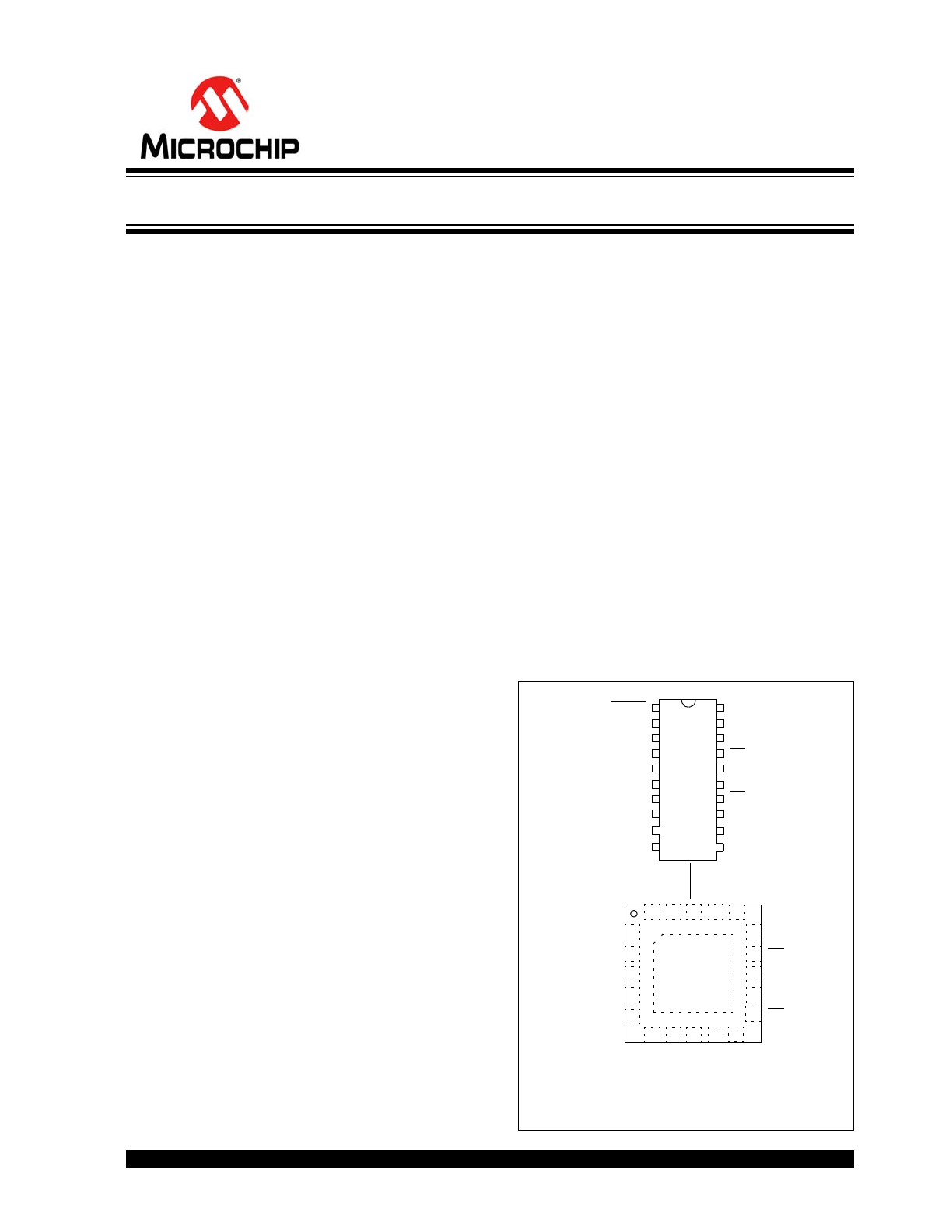
Package Type
OSC1/CLKI
1
2
3
4
20
19
18
17
16
15
14
13
5
6
7
8
OSC2
SDI
RESET
DV
DD
AV
DD
CH0+
CH0-
CH1-
12
9
DGND
MDAT0
MDAT1
DR
CH1+
AGND
SDO
11
10
REFIN/OUT+
REFIN-
CS
SCK
20-Lead SSOP
5
2
EP
20
1
19 18 17
3
4
15
14
13
12
6
7
8
9
21
10
11
16
CH0+
CH0-
CH1-
CH1+
AGND
REF
IN-
REF
IN/OUT
+
DG
ND
MD
A
T
1
MD
A
T
0
OSC1/CLKI
OSC2
DR
CS
SCK
SDO
SD
I
RES
E
T
DV
DD
AV
DD
20-Lead QFN
* Includes Exposed Thermal Pad (EP); see
Table 3-1
.
Two-Channel Analog Front End
MCP3901
DS22192D-page 2
© 2011 Microchip Technology Inc.
Functional Block Diagram
CH0+
CH0-
CH1+
CH1-
SDO
SDI
SCK
DUAL DS ADC
SINC
3
-
+
PGA
Xtal Oscillator
MCLK
OSC1
OSC2
DR
RESET
Digital SPI
Interface
Clock
Generation
SINC
3
-
+
PGA
Modulator
AMCLK
DMCLK/DRCLK
Modulator
Output Block
MDAT1
MDAT0
DMCLK
Phase
Shifter
PHASE <7:0>
OSR<1:0>
PRE<1:0>
DATA_CH0<23:0>
DATA_CH1<23:0>
MODOUT<1:0>
MOD<7:0>
CS
REFIN/OUT+
REFIN -
AV
DD
AGND
DGND
DV
DD
POR
AV
DD
Monitoring
POR
Modulator
V
REF
+
V
REF
-
VREFEXT
Voltage
Reference
V
REF
+
-
Δ -Σ
Δ -Σ
Φ
ANALOG DIGITAL
SDN<1:0>, RESET<1:0>, GAIN<7:0>
© 2011 Microchip Technology Inc.
DS22192D-page 3
MCP3901
1.0
ELECTRICAL
CHARACTERISTICS
Absolute Maximum Ratings †
V
DD
...................................................................................7.0V
Digital inputs and outputs w.r.t. A
GND
........ -0.6V to V
DD
+0.6V
Analog input w.r.t. A
GND
..................................... ....-6V to +6V
V
REF
input w.r.t. A
GND
............................... -0.6V to V
DD
+0.6V
Storage temperature .....................................-65°C to +150°C
Ambient temp. with power applied ................-65°C to +125°C
Soldering temperature of leads (10 seconds) ............. +300°C
ESD on the analog inputs (HBM,MM) ................. 7.0 kV, 400V
ESD on all other pins (HBM,MM) ........................ 7.0 kV, 400V
† Notice: Stresses above those listed under “Absolute
Maximum Ratings” may cause permanent damage to the
device. This is a stress rating only and functional operation of
the device at those or any other conditions, above those indi-
cated in the operational listings of this specification, is not
implied. Exposure to maximum rating conditions for extended
periods may affect device reliability.
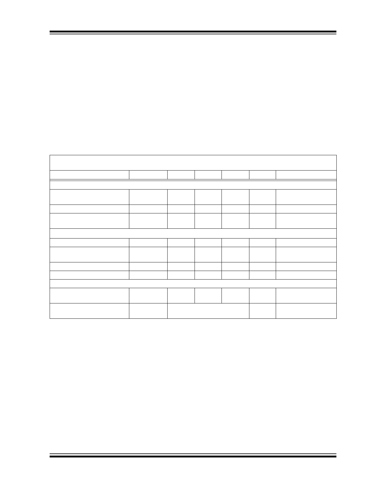
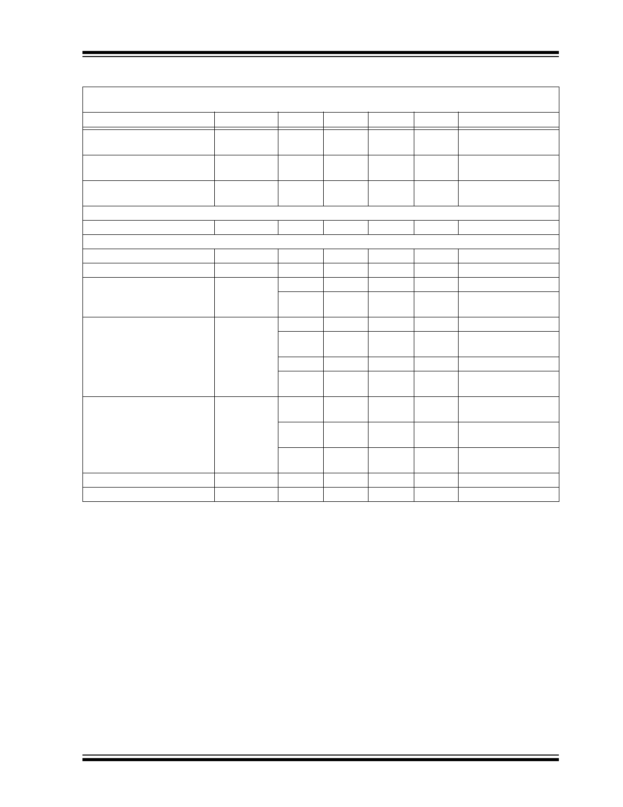
ELECTRICAL CHARACTERISTICS
Electrical Specifications: Unless otherwise indicated, AV
DD
= 4.5 to 5.5V, DV
DD
= 2.7 to 5.5V; -40°C < T
A
< +85°C,
MCLK = 4 MHz; PRESCALE = 1; OSR = 64; GAIN = 1; Dithering OFF; V
IN
= -0.5 dBFS = 333 mV
RMS
@ 50/60 Hz
Parameters
Symbol
Min
Typical
Max
Units
Conditions
Internal Voltage Reference
Internal Voltage Reference
Tolerance
V
REF
-2%
2.37
+2%
V
VREFEXT = 0
Temperature Coefficient
TC
REF
—
12
—
ppm/°C
VREFEXT = 0
Output Impedance
ZOUT
REF
—
7
—
k
Ω
AV
DD
= 5V,
VREFEXT = 0
Voltage Reference Input
Input Capacitance
—
—
10
pF
Differential Input Voltage Range
(V
REF+
– V
REF-
)
V
REF
2.2
—
2.6
V
V
REF
= (V
REF+
– V
REF-
),
VREFEXT = 1
Absolute Voltage on REFIN+ Pin
V
REF+
1.9
—
2.9
V
VREFEXT = 1
Absolute Voltage on REFIN- Pin
V
REF-
-0.3
—
0.3
V
ADC Performance
Resolution (No Missing Codes)
24
—
—
bits
OSR = 256
(See
Table 5-3
)
Sampling Frequency
f
S
See
Table 4-2
kHz
f
S
= DMCLK = MCLK/
(4 x PRESCALE)
Note 1:
This specification implies that the ADC output is valid over this entire differential range and that there is no
distortion or instability across this input range. Dynamic performance is specified at -0.5 dB below the
maximum signal range, V
IN
= -0.5 dBFS @ 50/60 Hz = 353 mV
RMS,
V
REF
= 2.4V.
2:
See terminology section for definition.
3:
This parameter is established by characterization and not 100% tested.
4:
For these operating currents, the following bit settings apply: SHUTDOWN<1:0> = 00, RESET<1:0> = 00,
VREFEXT = 0, CLKEXT = 0.
5:
For these operating currents, the following Configuration bit settings apply: SHUTDOWN<1:0> = 11,
VREFEXT = 1, CLKEXT = 1.
6:
Applies to all gains. Offset error is dependant on PGA gain setting (see
Figure 2-19
for typical values).
7:
Outside of this range, the ADC accuracy is not specified. An extended input range of ±6V can be applied
continuously to the part with no risk for damage.
8:
For proper operation and to keep ADC accuracy, AMCLK should always be in the range of 1 to 5 MHz with
BOOST bits off. With BOOST bits on, AMCLK should be in the range of 1 to 8.192 MHz,
AMCLK = MCLK/PRESCALE. When using a crystal, the CLKEXT bit should be equal to ‘0’.
MCP3901
DS22192D-page 4
© 2011 Microchip Technology Inc.
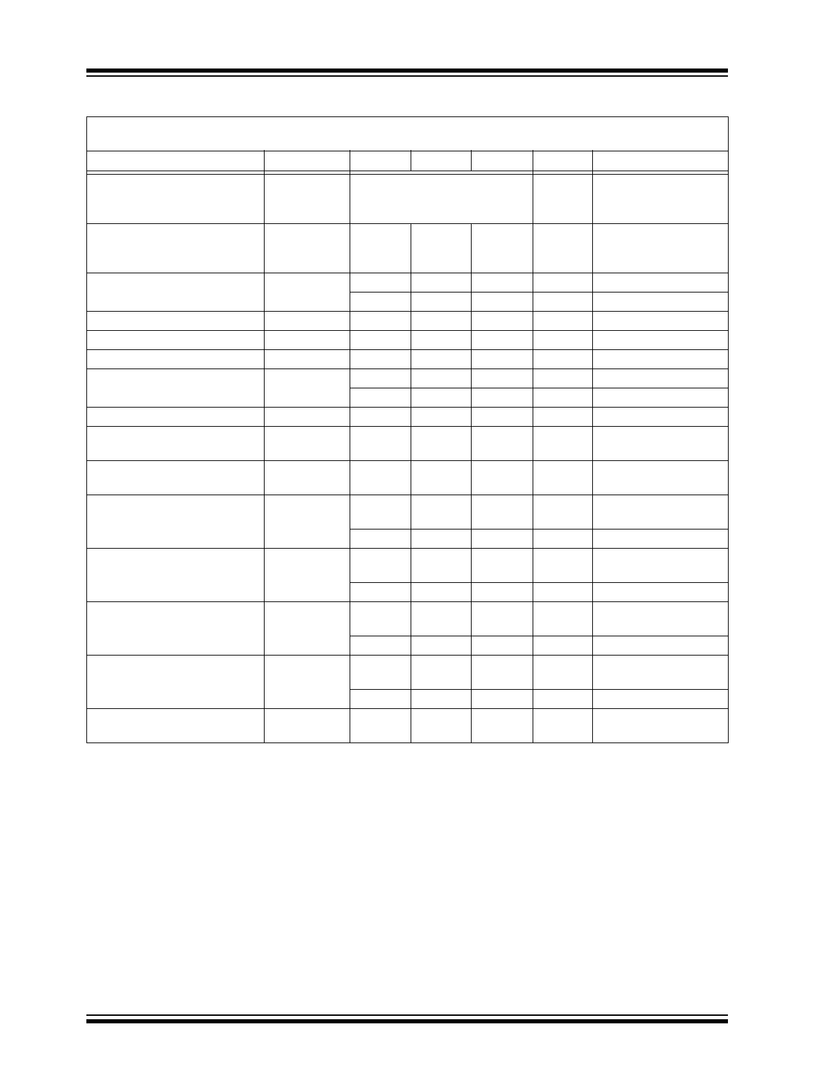
Output Data Rate
f
D
See
Table 4-2
ksps
f
D
= DRCLK = DMCLK/
OSR = MCLK/
(4 x PRESCALE x OSR)
Analog Input Absolute Voltage
on CH0+, CH0-, CH1+,
CH1- Pins
CHn+
-1
—
+1
V
All analog input
channels, measured to
AGND (
Note 7
)
Analog Input Leakage Current
A
IN
—
1
—
nA
(
Note 4
)
—
2
—
nA
-40°C < T
A
< 125°C
Differential Input Voltage Range (CHn+ – CHn-)
—
—
500/GAIN
mV
(
Note 1
)
Offset Error (
Note 2
)
V
OS
-3
—
+3
mV
(
Note 6
)
Offset Error Drift
—
3
—
µV/°C
From -40°C to +125°C
Gain Error (
Note 2
)
GE
—
-0.4
—
%
G = 1
-2.5
—
+2.5
%
All Gains
Gain Error Drift
—
1
—
ppm/°C
From -40°C to +125°C
Integral Nonlinearity (
Note 2
)
INL
—
15
—
ppm
GAIN = 1,
DITHER = On
Input Impedance
Z
IN
350
—
—
k
Ω
Proportional to
1/AMCLK
Signal-to-Noise and Distortion
Ratio (
Notes 2
,
3
)
SINAD
89
91
—
dB
OSR = 256,
DITHER = On
78
79
—
dB
Total Harmonic Distortion
(
Notes 2
,
3
)
THD
—
-104
-102
dB
OSR = 256,
DITHER = On
—
-85
-84
dB
Signal-to-Noise Ratio
(
Notes 2
,
3
)
SNR
89
91
—
dB
OSR = 256,
DITHER = On
80
81
—
dB
Spurious Free Dynamic Range
(
Note 2
)
SFDR
—
109
—
dB
OSR = 256,
DITHER = On
—
87
—
dB
Crosstalk (50/60 Hz) (
Note 2
)
CTALK
—
-133
—
dB
OSR = 256,
DITHER = On
ELECTRICAL CHARACTERISTICS (CONTINUED)
Electrical Specifications: Unless otherwise indicated, AV
DD
= 4.5 to 5.5V, DV
DD
= 2.7 to 5.5V; -40°C < T
A
< +85°C,
MCLK = 4 MHz; PRESCALE = 1; OSR = 64; GAIN = 1; Dithering OFF; V
IN
= -0.5 dBFS = 333 mV
RMS
@ 50/60 Hz
Parameters
Symbol
Min
Typical
Max
Units
Conditions
Note 1:
This specification implies that the ADC output is valid over this entire differential range and that there is no
distortion or instability across this input range. Dynamic performance is specified at -0.5 dB below the
maximum signal range, V
IN
= -0.5 dBFS @ 50/60 Hz = 353 mV
RMS,
V
REF
= 2.4V.
2:
See terminology section for definition.
3:
This parameter is established by characterization and not 100% tested.
4:
For these operating currents, the following bit settings apply: SHUTDOWN<1:0> = 00, RESET<1:0> = 00,
VREFEXT = 0, CLKEXT = 0.
5:
For these operating currents, the following Configuration bit settings apply: SHUTDOWN<1:0> = 11,
VREFEXT = 1, CLKEXT = 1.
6:
Applies to all gains. Offset error is dependant on PGA gain setting (see
Figure 2-19
for typical values).
7:
Outside of this range, the ADC accuracy is not specified. An extended input range of ±6V can be applied
continuously to the part with no risk for damage.
8:
For proper operation and to keep ADC accuracy, AMCLK should always be in the range of 1 to 5 MHz with
BOOST bits off. With BOOST bits on, AMCLK should be in the range of 1 to 8.192 MHz,
AMCLK = MCLK/PRESCALE. When using a crystal, the CLKEXT bit should be equal to ‘0’.
© 2011 Microchip Technology Inc.
DS22192D-page 5
MCP3901
AC Power Supply Rejection
AC PSRR
—
-77
—
dB
AV
DD
and DV
DD
= 5V +
1 V
PP
@ 50/60 Hz
DC Power Supply Rejection
DC PSRR
—
-77
—
dB
AV
DD
and DV
DD
= 4.5 to
5.5V
DC Common-Mode Rejection
Ratio (
Note 2
)
CMRR
—
-72
—
dB
V
CM
varies from -1V to
+1V
Oscillator Input
Master Clock Frequency Range
MCLK
1
—
16.384
MHz
(
Note 8
)
Power Specifications
Operating Voltage, Analog
AV
DD
4.5
—
5.5
V
Operating Voltage, Digital
DV
DD
2.7
3.6
5.5
V
Power On Reset Threshold
POR
—
4.2
—
V
(
Note 3
)
—
4.6
—
-40°C < T
A
< 125°C,
(
Note 3
)
Operating Current, Analog
(
Note 4
)
AI
DD
—
2.1
2.8
mA
BOOST<1:0> = 00
—
2.1
3.3
mA
-40°C < T
A
< 125°C,
BOOST<1:0> = 00
—
3.8
5.6
mA
BOOST<1:0> = 11
—
3.8
7
mA
-40°C < T
A
< 125°C,
BOOST<1:0> = 11
Operating Current, Digital
DI
DD
—
0.45
1.0
mA
DV
DD
= 5V,
MCLK = 4 MHz
—
0.25
0.45
mA
DV
DD
= 2.7V,
MCLK = 4 MHz
—
1.2
1.6
mA
DV
DD
= 5V,
MCLK = 8.192 MHz
Shutdown Current, Analog
I
DDS,A
—
—
1
µA
AV
DD
pin only (
Note 5
)
Shutdown Current, Digital
I
DDS,D
—
—
1
µA
DV
DD
pin only (
Note 5
)
ELECTRICAL CHARACTERISTICS (CONTINUED)
Electrical Specifications: Unless otherwise indicated, AV
DD
= 4.5 to 5.5V, DV
DD
= 2.7 to 5.5V; -40°C < T
A
< +85°C,
MCLK = 4 MHz; PRESCALE = 1; OSR = 64; GAIN = 1; Dithering OFF; V
IN
= -0.5 dBFS = 333 mV
RMS
@ 50/60 Hz
Parameters
Symbol
Min
Typical
Max
Units
Conditions
Note 1:
This specification implies that the ADC output is valid over this entire differential range and that there is no
distortion or instability across this input range. Dynamic performance is specified at -0.5 dB below the
maximum signal range, V
IN
= -0.5 dBFS @ 50/60 Hz = 353 mV
RMS,
V
REF
= 2.4V.
2:
See terminology section for definition.
3:
This parameter is established by characterization and not 100% tested.
4:
For these operating currents, the following bit settings apply: SHUTDOWN<1:0> = 00, RESET<1:0> = 00,
VREFEXT = 0, CLKEXT = 0.
5:
For these operating currents, the following Configuration bit settings apply: SHUTDOWN<1:0> = 11,
VREFEXT = 1, CLKEXT = 1.
6:
Applies to all gains. Offset error is dependant on PGA gain setting (see
Figure 2-19
for typical values).
7:
Outside of this range, the ADC accuracy is not specified. An extended input range of ±6V can be applied
continuously to the part with no risk for damage.
8:
For proper operation and to keep ADC accuracy, AMCLK should always be in the range of 1 to 5 MHz with
BOOST bits off. With BOOST bits on, AMCLK should be in the range of 1 to 8.192 MHz,
AMCLK = MCLK/PRESCALE. When using a crystal, the CLKEXT bit should be equal to ‘0’.
MCP3901
DS22192D-page 6
© 2011 Microchip Technology Inc.
SERIAL INTERFACE SPECIFICATIONS
Electrical Specifications: Unless otherwise indicated, all parameters apply: AV
DD
= 4.5 to 5.5V, DV
DD
= 2.7 to 5.5V,
-40°C < T
A
< +85°C, C
LOAD
= 30 pF
Parameters
Sym
Min
Typ
Max
Units
Conditions
Serial Clock Frequency
f
SCK
—
—
—
—
20
10
MHz
MHz
4.5
≤ DV
DD
≤ 5.5
2.7
≤ DV
DD
< 5.5
CS Setup Time
t
CSS
25
50
—
—
—
—
ns
ns
4.5
≤ DV
DD
≤ 5.5
2.7
≤ DV
DD
≤ 5.5
CS Hold Time
t
CSH
50
100
—
—
—
—
ns
ns
4.5
≤ DV
DD
≤ 5.5
2.7
≤ DV
DD
< 5.5
CS Disable Time
t
CSD
50
—
—
ns
Data Setup Time
t
SU
5
10
—
—
—
—
ns
ns
4.5
≤ DV
DD
≤ 5.5
2.7
≤ DV
DD
< 5.5
Data Hold Time
t
HD
10
20
—
—
—
—
ns
ns
4.5
≤ DV
DD
≤ 5.5
2.7
≤ DV
DD
< 5.5
Serial Clock High Time
t
HI
20
50
—
—
—
—
ns
ns
4.5
≤ DV
DD
≤ 5.5
2.7
≤ DV
DD
< 5.5
Serial Clock Low Time
t
LO
20
50
—
—
—
—
ns
ns
4.5
≤ DV
DD
≤ 5.5
2.7
≤ DV
DD
< 5.5
Serial Clock Delay Time
t
CLD
50
—
—
ns
Serial Clock Enable Time
t
CLE
50
—
—
ns
Output Valid from SCK Low
t
DO
—
—
50
ns
2.7
≤ DV
DD
< 5.5
Modulator Output Valid from AMCLK
High
t
DOMDAT
—
—
1/2 * AMCLK
s
Output Hold Time
t
HO
0
—
—
ns
(
Note 1
)
Output Disable Time
t
DIS
—
—
—
—
25
50
ns
ns
4.5
≤ DV
DD
≤ 5.5
2.7
≤ DV
DD
< 5.5 (
Note 1
)
Reset Pulse Width (RESET)
t
MCLR
100
—
—
ns
2.7
≤ DV
DD
< 5.5
Data Transfer Time to DR (data ready)
t
DODR
—
—
50
ns
2.7
≤ DV
DD
< 5.5
Data Ready Pulse Low Time
t
DRP
—
1/DMCLK
—
µs
2.7
≤ DV
DD
< 5.5
Schmitt Trigger High-Level Input Voltage
V
IH1
.7 DV
DD
—
DV
DD
+ 1
V
Schmitt Trigger Low-Level Input Voltage
V
IL1
-0.3
—
0.2 DV
DD
V
Hysteresis of Schmitt Trigger Inputs
(all digital inputs)
V
HYS
300
—
—
mV
Low-Level Output Voltage, SDO Pin
V
OL
—
—
0.4
V
SDO pin only,
I
OL
= +2.0 mA, V
DD
= 5.0V
Low-level output voltage, DR and
MDAT Pins
V
OL
—
—
0.4
V
DR and MDAT pins only,
I
OL
= +800 mA, V
DD
= 5.0V
High-level output voltage, SDO pin
V
OH
DV
DD
– 0.5
—
—
V
SDO pin only,
I
OH
= -2.0 mA, V
DD
= 5.0V
High-level output voltage, DR and
MDAT pins
V
OH
DV
DD
– 0.5
—
—
V
DR and MDAT pins only,
I
OH
= -800 µA, V
DD
= 5.0V
Input leakage current
I
LI
—
—
±1
µA
CS = DV
DD
,
V
IN
= DGND or DV
DD
Output leakage current
I
LO
—
—
±1
µA
CS = DV
DD
,
V
OUT
= DGND or DV
DD
Internal capacitance (all inputs and
outputs)
C
INT
—
—
7
pF
T
A
= 25°C,
SCK = 1.0 MHz,
DV
DD
= 5.0V (
Note 1
)
Note
1:
This parameter is periodically sampled and not 100% tested.
© 2011 Microchip Technology Inc.
DS22192D-page 7
MCP3901
FIGURE 1-1:
Serial Output Timing Diagram.
FIGURE 1-2:
Serial Input Timing Diagram.
TEMPERATURE CHARACTERISTICS
Electrical Specifications: Unless otherwise indicated, all parameters apply at AV
DD
= 4.5 to 5.5V,
DV
DD
= 2.7 to 5.5V
Parameters
Sym
Min
Typ
Max
Units
Conditions
Temperature Ranges
Operating Temperature Range
T
A
-40
—
+125
°C
(
Note 1
)
Storage Temperature Range
T
A
-65
—
+150
°C
Thermal Package Resistances
Thermal Resistance, 20L SSOP
θ
JA
—
89.3
—
°C/W
Thermal Resistance, 20L QFN
θ
JA
—
43
—
°C/W
Note 1:
The internal junction temperature (T
J
) must not exceed the absolute maximum specification of +150°C.
t
CSH
t
DIS
t
HI
t
LO
f
SCK
CS
SCK
SDO
MSB Out
LSB Out
Don’t Care
SDI
Mode 1,1
Mode 0,0
t
HO
t
DO
CS
SCK
SDI
LSB In
MSB In
Mode 1,1
Mode 0,0
t
CSS
t
SU
t
HD
t
CSD
t
CSH
t
CLD
t
CLE
SDO
HI-Z
t
HI
t
LO
f
SCK
MCP3901
DS22192D-page 8
© 2011 Microchip Technology Inc.
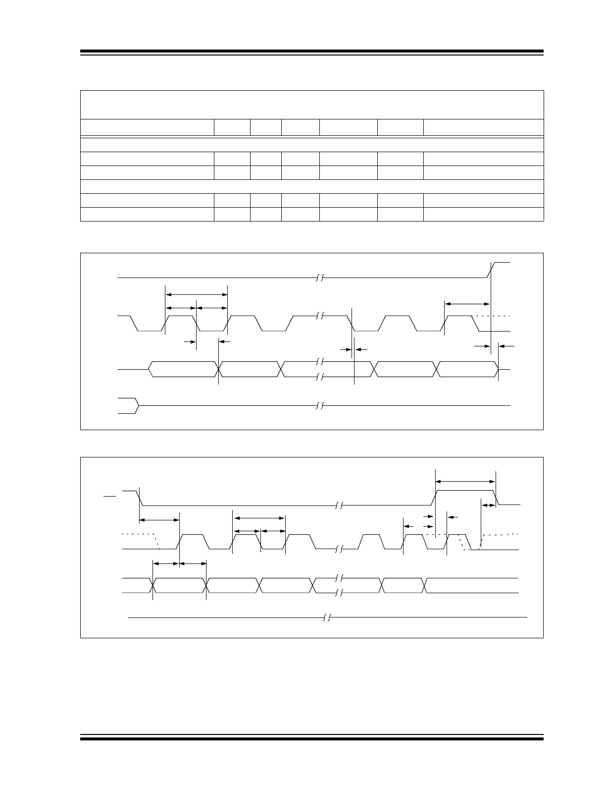
FIGURE 1-3:
Data Ready Pulse Timing Diagram.
H
FIGURE 1-4:
Specific Timing Diagrams.
FIGURE 1-5:
MCP3901 Clock Detail.
DR
SCK
SDO
1/DRCLK
t
DODR
t
DRP
CS
V
IH
Timing Waveform for t
DIS
HI-Z
90%
10%
t
DIS
SDO
SCK
SDO
t
DO
Timing Waveform for t
DO
MDAT0/1
OSC1/CLKI
Timing Waveform for MDAT0/1
Modulator Output
t
DOMDAT
CLKEXT
1
0
PRESCALE<1:0>
1/
MCLK
AMCLK
1/4
DMCLK
1/OSR
DRCLK
OSR<1:0>
Multiplexer
Clock Divider
Clock Divider
Clock Divider
Crystal
Oscillator
OSC1
OSC2
1/Prescale
f
S
ADC
Sampling
Rate
f
D
ADC
Output
Data Rate
Digital Buffer
© 2011 Microchip Technology Inc.
DS22192D-page 9
MCP3901
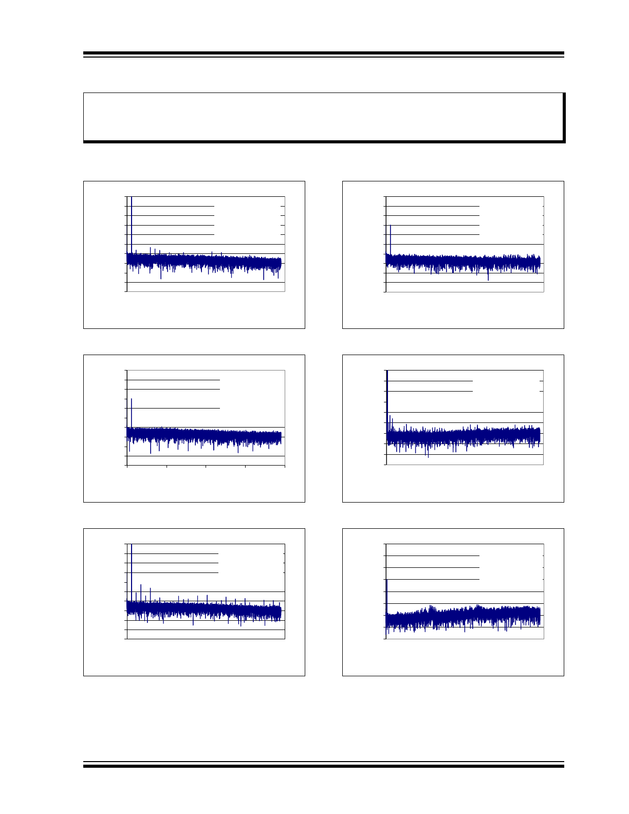
2.0
TYPICAL PERFORMANCE CURVES
Note:
Unless otherwise indicated, AV
DD
= 5.0V, DV
DD
= 5.0V; T
A
= +25°C, MCLK = 4 MHz; PRESCALE = 1;
OSR = 64; GAIN = 1; Dithering OFF; V
IN
= -0.5 dBFS @ 60 Hz.
FIGURE 2-1:
Spectral Response.
FIGURE 2-2:
Spectral Response.
FIGURE 2-3:
Spectral Response.
FIGURE 2-4:
Spectral Response.
FIGURE 2-5:
Spectral Response.
FIGURE 2-6:
Spectral Response.
Note:
The graphs and tables provided following this note are a statistical summary based on a limited number of
samples and are provided for informational purposes only. The performance characteristics listed herein
are not tested or guaranteed. In some graphs or tables, the data presented may be outside the specified
operating range (e.g., outside specified power supply range) and therefore, outside the warranted range.
-200
-180
-160
-140
-120
-100
-80
-60
-40
-20
0
0
500
1000
1500
2000
Frequency (Hz)
A
m
plitu
d
e
(
d
B
)
f
IN
= -0.5dBFS @ 60 Hz
f
D
= 3.9 ksps
16384 Point FFT
OSR = 256
Dithering ON
-200
-180
-160
-140
-120
-100
-80
-60
-40
-20
0
0
500
1000
1500
2000
Frequency (Hz)
Am
p
li
tu
d
e
(
d
B
)
f
IN
= -60dBFS @ 60 Hz
f
D
= 3.9 ksps
16384 Point FFT
OSR = 256
Dithering ON
-200
-180
-160
-140
-120
-100
-80
-60
-40
-20
0
0
500
1000
1500
2000
Frequency (Hz)
A
m
plitu
d
e
(
d
B
)
f
IN
= -0.5dBFS @ 60 Hz
f
D
= 3.9 ksps
OSR = 256
16384 points
Dithering OFF
-200
-180
-160
-140
-120
-100
-80
-60
-40
-20
0
0
500
1000
1500
2000
Frequency (Hz)
A
m
plitu
d
e
(
d
B
)
f
IN
= -60dBFS @ 60 Hz
f
D
= 3.9 ksps
16384 Point FFT
OSR = 256
Dithering OFF
-180
-160
-140
-120
-100
-80
-60
-40
-20
0
0
2000
4000
6000
8000
Frequency (Hz)
A
m
pl
it
ud
e
(
d
B
)
f
IN
= -0.5dBFS @ 60 Hz
f
D
= 15.6 ksps
16384 Point FFT
OSR = 64
Dithering OFF
-160
-140
-120
-100
-80
-60
-40
-20
0
0
2000
4000
6000
8000
Frequency (Hz)
A
m
plitu
d
e
(
d
B
)
f
IN
= -60dBFS @ 60 Hz
f
D
= 15.6 ksps
16384 Point FFT
OSR = 64
Dithering OFF
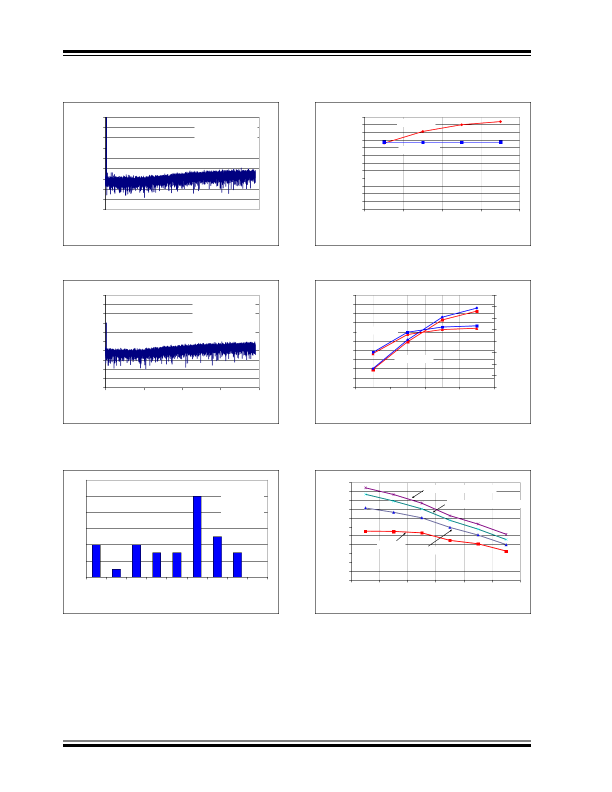
MCP3901
DS22192D-page 10
© 2011 Microchip Technology Inc.
Note:
Unless otherwise indicated, AV
DD
= 5.0V, DV
DD
= 5.0V; T
A
= +25°C, MCLK = 4 MHz; PRESCALE = 1;
OSR = 64; GAIN = 1; Dithering OFF; V
IN
= -0.5 dBFS @ 60 Hz.
FIGURE 2-7:
Spectral Response.
FIGURE 2-8:
Spectral Response.
FIGURE 2-9:
Spurious Free Dynamic
Range Histogram.
FIGURE 2-10:
Spurious Free Dynamic
Range vs. Oversampling Ratio.
FIGURE 2-11:
Signal-to-Noise and
Distortion and Effective Number of Bits vs.
Oversampling Ratio.
FIGURE 2-12:
Signal-to-Noise and
Distortion vs. Gain.
-180
-160
-140
-120
-100
-80
-60
-40
-20
0
0
2000
4000
6000
8000
Frequency (Hz)
Am
p
li
tu
d
e
(
d
B
)
f
IN
= -0.5dBFS @ 60 Hz
f
D
= 15.6 ksps
16384 Point FFT
OSR = 64
Dithering ON
-200
-180
-160
-140
-120
-100
-80
-60
-40
-20
0
0
2000
4000
6000
8000
Frequency (Hz)
Am
p
li
tu
d
e
(
d
B
)
f
IN
= -60dBFS @ 60 Hz
f
D
= 15.6 ksps
16384 Point FFT
OSR = 64
Dithering ON
0
2
4
6
8
1
0
1
2
107 107.5 108 108.5 109 109.5 110 110.5 111
Spurious Free Dynamic Range (dB)
Fr
e
q
ue
nc
y
of
O
c
c
u
ra
nc
e
f
IN
= 60 Hz
MCLK = 4 MHz
OSR = 256
Dithering On
0
10
20
30
40
50
60
70
80
90
100
110
120
32
64
128
256
Oversampling Ratio (OSR)
S
pur
io
us
Fr
e
e
D
y
na
mi
c
Ra
n
g
e
(
d
B)
Dithering OFF
Dithering ON
50
55
60
65
70
75
80
85
90
95
100
32
64
128
256
Oversampling Ratio (OSR)
S
INAD (
d
B)
8
9
10
11
12
13
14
15
16
E
ff
e
c
ti
ve N
u
m
b
er
o
f
B
it
s
Dithering ON
Dithering OFF
40
45
50
55
60
65
70
75
80
85
90
95
1
2
4
8
16
32
Gain (V/V)
S
INAD (
d
B
)
OSR = 256 (Dithering ON)
OSR = 32
OSR = 64
OSR = 128 (Dithering ON)