

SMSC TMC2084
Page 1
Revision 0.2 (10-23-08)
DATASHEET
TMC2084
Standalone Mode
CircLink
TM
Controller
Datasheet
PRODUCT FEATURES
Low Power CMOS, 3.3 Volt Power Supply with 5
Volt Tolerant I/O
Enhanced Token Passing Protocol from ARCNET
− Maximum 15 node per network
− Token Retry Mechanism
− 64/128 Byte Per Packet
− Consecutive Node ID Assignment
Memory Mirror
− Shared Memory Within Network
Network Standard Time
− Network Time Synchronization
− Automatic Time Stamping
Coded Mark Inversion
− Intelligent 1-Bit Error Correction
− Magnetic Saturation Prevention
Standalone I/O Mode Operates without MCU
− Supports 16 Bit Input and 16 Bit Output
Up to 14 Intelligent Remote I/O Ports:
− Programmable with 8-bit basis (16 to 32 outputs; 0 to
16 inputs)
− Selectable output type (push-pull or open-drain)
− The part of port is definable as strobe outputs and/or
external trigger inputs
− The anti-chatter circuit on the input port can be set in
ON/OFF
− The sampling frequency of the anti-chatter circuit can
be set (19.1Hz/1.22KHz)
Feature Rich Transmit Trigger:
− After receiving OUTPUT DATA packet or expiring on-
chip timer
− Continuous transmission
− External trigger input
Flexible Transceiver Interface:
− RS-485 transceiver + twist pair cable
− RS-485 transceiver + pulse transformer + twist pair
cable
− Hybrid transceiver (HYC4000 or HYC2000 from
SMSC Japan)
− Fiber Optics also supported
48-Pin, TQFP Lead-Free RoHS Compliant
Package
− Body size: 7 × 7mm; pitch: 0.5mm
Temperature Range from 0 to 70 degrees C

Standalone Mode CircLink
TM
Controller
Datasheet
Revision 0.2 (10-23-08)
Page 2
SMSC TMC2084
DATASHEET
ORDERING INFORMATION
Order Number(s):
TMC2084-HT for 48 pin, TQFP Lead-Free RoHS Compliant Package
80 ARKAY DRIVE, HAUPPAUGE, NY 11788 (631) 435-6000, FAX (631) 273-3123
Copyright © 2008 SMSC or its subsidiaries. All rights reserved.
Circuit diagrams and other information relating to SMSC products are included as a means of illustrating typical applications. Consequently, complete
information sufficient for construction purposes is not necessarily given. Although the information has been checked and is believed to be accurate, no
responsibility is assumed for inaccuracies. SMSC reserves the right to make changes to specifications and product descriptions at any time without
notice. Contact your local SMSC sales office to obtain the latest specifications before placing your product order. The provision of this information
does not convey to the purchaser of the described semiconductor devices any licenses under any patent rights or other intellectual property rights of
SMSC or others. All sales are expressly conditional on your agreement to the terms and conditions of the most recently dated version of SMSC's
standard Terms of Sale Agreement dated before the date of your order (the "Terms of Sale Agreement"). The product may contain design defects or
errors known as anomalies which may cause the product's functions to deviate from published specifications. Anomaly sheets are available upon
request. SMSC products are not designed, intended, authorized or warranted for use in any life support or other application where product failure
could cause or contribute to personal injury or severe property damage. Any and all such uses without prior written approval of an Officer of SMSC
and further testing and/or modification will be fully at the risk of the customer. Copies of this document or other SMSC literature, as well as the Terms
of Sale Agreement, may be obtained by visiting SMSC’s website at http://www.smsc.com. SMSC is a registered trademark of Standard Microsystems
Corporation (“SMSC”). Product names and company names are the trademarks of their respective holders.
SMSC DISCLAIMS AND EXCLUDES ANY AND ALL WARRANTIES, INCLUDING WITHOUT LIMITATION ANY AND ALL IMPLIED WARRANTIES
OF MERCHANTABILITY, FITNESS FOR A PARTICULAR PURPOSE, TITLE, AND AGAINST INFRINGEMENT AND THE LIKE, AND ANY AND
ALL WARRANTIES ARISING FROM ANY COURSE OF DEALING OR USAGE OF TRADE. IN NO EVENT SHALL SMSC BE LIABLE FOR ANY
DIRECT, INCIDENTAL, INDIRECT, SPECIAL, PUNITIVE, OR CONSEQUENTIAL DAMAGES; OR FOR LOST DATA, PROFITS, SAVINGS OR
REVENUES OF ANY KIND; REGARDLESS OF THE FORM OF ACTION, WHETHER BASED ON CONTRACT; TORT; NEGLIGENCE OF SMSC
OR OTHERS; STRICT LIABILITY; BREACH OF WARRANTY; OR OTHERWISE; WHETHER OR NOT ANY REMEDY OF BUYER IS HELD TO
HAVE FAILED OF ITS ESSENTIAL PURPOSE, AND WHETHER OR NOT SMSC HAS BEEN ADVISED OF THE POSSIBILITY OF SUCH
DAMAGES.

Standalone Mode CircLink
TM
Controller
Datasheet
SMSC TMC2084
Page 3
Revision 0.2 (10-23-08)
DATASHEET
Table of Contents
Chapter 1
General Description ............................................................................................................. 5
1.1
About CircLink ..................................................................................................................................... 5
1.2
About TMC2084 .................................................................................................................................. 5
1.3
Block Diagram ..................................................................................................................................... 7
1.4
Pin List................................................................................................................................................. 8
1.5
Pinout ................................................................................................................................................ 12
Chapter 2
Functional Description....................................................................................................... 13
2.1
Network Configuration....................................................................................................................... 13
2.1.1
General...................................................................................................................................................13
2.1.2
Configuration Examples..........................................................................................................................15
2.2
Initial Configuration............................................................................................................................ 16
2.2.1
Configuration Using Shared Pins............................................................................................................16
2.2.2
Configuration Through the Network ........................................................................................................21
2.2.3
Returning Configuration Data .................................................................................................................29
2.3
Types of Packets............................................................................................................................... 30
2.3.1
Packets TMC2084 Can Receive.............................................................................................................30
2.3.2
Packets TMC2084 Can Transmit............................................................................................................31
2.4
Command Packets ............................................................................................................................ 32
2.4.1
Format of COMMAND Packets...............................................................................................................32
2.5
OUTPUT PORTs............................................................................................................................... 34
2.5.1
Format of OUTPUT DATA Packets ........................................................................................................35
2.5.2
Configuring I/O Port Directions ...............................................................................................................36
2.5.3
Open-Drain Mode ...................................................................................................................................36
2.5.4
Initializing OUTPUT PORTs ...................................................................................................................36
2.5.5
Switching Timing In OUTPUT PORTs ....................................................................................................36
2.6
INPUT PORT..................................................................................................................................... 37
2.6.1
Format of Input Data Packets .................................................................................................................38
2.7
FLAG OUTPUT ................................................................................................................................. 40
2.7.1
Flag Descriptions ....................................................................................................................................41
2.7.2
Pulse Level Width Of Each Output Flag .................................................................................................42
2.8
Status Bits ......................................................................................................................................... 42
2.9
NST Time Stamps ............................................................................................................................. 45
2.9.1
Time Synchronization .............................................................................................................................46
2.9.2
Carry Output ...........................................................................................................................................46
2.10
CMI Coding .................................................................................................................................... 48
2.11
RAM Image On Host Side.............................................................................................................. 48
2.12
Configuration Flow ......................................................................................................................... 51
Chapter 3
Operating Conditions......................................................................................................... 53
3.1
Absolute Maximum Ratings .............................................................................................................. 53
3.2
Typical Operating Conditions ............................................................................................................ 53
3.3
DC Characteristics ............................................................................................................................ 53
3.4
AC Characteristics............................................................................................................................. 55
3.4.1
Timing Measurement Points ...................................................................................................................55
3.4.2
CMI Transmit And Receive Waveforms (nCMIBYP = H) ........................................................................56
3.4.3
RZ Transmit And Receive Waveforms (nCMIBYP = L) ..........................................................................57
3.4.4
External Trigger Input .............................................................................................................................57
3.4.5
Other Timing Specifications....................................................................................................................58
3.5
Package Outline ................................................................................................................................ 59
3.6
Device Marking.................................................................................................................................. 61
3.7
Oscillator Circuit ................................................................................................................................ 62
3.8
Basic Device Connections ................................................................................................................ 63

Standalone Mode CircLink
TM
Controller
Datasheet
Revision 0.2 (10-23-08)
Page 4
SMSC TMC2084
DATASHEET
Chapter 4
APPENDIX ......................................................................................................................... 64
4.1
Application Circuit Examples............................................................................................................. 64
4.1.1
Connecting A/D and D/A.........................................................................................................................64
4.1.2
Connecting Watchdog Timer ..................................................................................................................65
4.1.3
Using SLT4 Plus RS485 .........................................................................................................................65
4.1.4
Considerations for Shared Pins When Port D is Configured as INPUT PORT .......................................66
4.1.5
Case Where Port A and B are Unused ...................................................................................................67
4.1.6
Case Where Port C is Unused................................................................................................................68
4.1.7
Case Where Port D is Unused................................................................................................................68
4.1.8
Initial Configuration for OUTPUT PORT (LED Display Example) ...........................................................69
4.1.9
Width of Reset Signal .............................................................................................................................70
4.2
Output Current from Shared Pins...................................................................................................... 72
4.3
Values of Pull-Up and Pull-Down Resisters......................................................................................73
List of Figures
Figure 1 -
TMC2084 Block Diagram..........................................................................................................................7
Figure 2 -
TMC2084 Pin Configuration....................................................................................................................12
Figure 3 -
Network Configuration Example 1: S Single Host and 15 Nodes............................................................15
Figure 4 -
Network Configuration Example 2: Dual Hosts and 6 Nodes ..................................................................15
Figure 5 -
Functional Diagram Of FLAG OUTPUT..................................................................................................40
Figure 6 -
Functional Diagram of NST Carry Output Generation Section................................................................46
Figure 7 -
nNSTCOUT Output Timing Example For Bits NSTC3 - 0 = 2h...............................................................47
Figure 8 -
State Transition Diagram for CMI ...........................................................................................................48
Figure 9 -
Initialization Procedure ...........................................................................................................................51
Figure 10 -
Procedure to change the configuration through the network during operation ....................................52
Figure 11 -
Input Signal Measurement Points .......................................................................................................55
List of Tables
Table 1 -
Truth Table Of Bits FOSL3 - 0 ................................................................................................................40
Table 2 -
Bits NSTPRE2 – 0 And NST Resolution.................................................................................................46
Table 3 -
Bits NSTC3 – 0 vs. Carry Output Bit.......................................................................................................47
Table 4 -
CircLink Controller Comparison Table ....................................................................................................74

Standalone Mode CircLink
TM
Controller
Datasheet
SMSC TMC2084
Page 5
Revision 0.2 (10-23-08)
DATASHEET
Chapter 1
General Description
1.1 About
CircLink
The CircLink networking controller was developed for small control-oriented local network data
communication based on ARCNET’s token-passing protocol that guarantees message integrity and
calculatable maximum delivery times.
In a CircLink network, when a node receives the token it becomes the temporary master of the network for
a fixed, short period of time. No node can dominate the network since token control must be relinquished
when transmission is complete. Once a transmission is completed the token is passed on to the next node
(logical neighbor), allowing it to be come the master.
Because of this token passing scheme, maximum waiting time for network access can be calculated and
the time performance of the network is predictable or deterministic. Industrial network applications require
predictable performance to ensure that controlled events occur when required.
However, reconfiguration of a regular ARCNET network becomes necessary when the token is missed due
to electronic and magnetic noise. In these cases, the maximum wait time for sending datagrams can not be
guaranteed and the real-time characteristic is impaired. CircLink makes several modification to the original
ARCNET protocol (such as maximum and consecutive node ID assignment) to avoid token missing as
much as possible and reduce the network reconfiguration time.
CircLink implements other enhancements to the ARCNET protocol including a smaller-sized network ,
shorter packet size, and remote buffer mode operation that enable more efficient and reliable small,
control-oriented LANs. In addition, CircLink introduces several unique features for reducing overall system
cost while increasing system reliability.
CircLink can operate under a special mode called “Standalone” or “I/O” mode. In this mode, CircLink does
not need an administrating CPU for each node. Only one CPU is needed to manage a CircLink network
composed of several nodes, reducing cost and complexity.
In a CircLink network, the data sent by the source node is received by all other nodes in the network and
stored according to node source ID. For the target node the received data is executed per ARCNET flow
control and the data is stored in its buffer RAM. The receiving node processes the data while the remaining
nodes on the network discard the data when the receiving node has completed. This memory-mirroring
function assures higher reliability and significantly reduces network traffic.
Network Standard Time (NST) is also a unique CircLink feature. NST is realized by synchronizing the
individual local time on each network node to the clock master in the designated node from which the
packet is sent. CircLink also uses CMI code for transmitting signals, rather than the dipulse or bipolar
signals that are the standard ARCNET signals. Since CMI encoding eliminates the DC element, a simple
combination of a standard RS485 IC and a pulse transformer can be used to implement a transformer-
coupled network.
1.2
About TMC2084
The TMC2084 is CircLink’s standalone mode controller acting as an intelligent remote I/O controller that
uses the enhanced token passing protocol. TMC2084 I/O nodes are controlled by the Host node
(TMC2074/72) via the network. Thus, TMC2084 enables a single-processor with multi-remote I/O
controllers environment at reasonable cost.

Standalone Mode CircLink
TM
Controller
Datasheet
Revision 0.2 (10-23-08)
Page 6
SMSC TMC2084
DATASHEET
The TMC2084 has thirty-two I/O port lines featuring programmable direction, with 8-bit basis (output: 16 to
32 bit; input: 0 to 16 bit). The maximum number of nodes per network is fifteen, including the host node.
This configuration enables a processor to control a total of 448 (14
× 32) remote I/O lines.
The Output Port type is selectable from either open-drain or push-pull, while one part of the I/O ports is
definable as either output pins for network status monitoring, strobe output pins to handshake with AD or
DA converter, or input pins for external trigger.
TMC2084 also has additional functions including the function to notify the host of its status, the states of its
Output Ports and settings, the function to send packets with timestamp, and the function to synchronize
the on-chip timer to the host.
This rich feature set is contained in a single 48-pin TQFP package.
Standalone Mode CircLink
TM
Controller
Datasheet
SMSC TMC2084
Page 7
Revision 0.2 (10-23-08)
DATASHEET
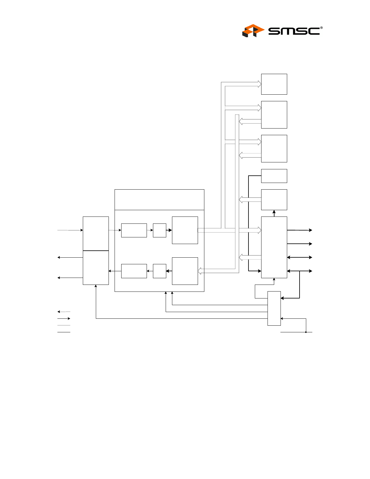
1.3 Block
Diagram
General
Purpose
I/O
NST
Time
Stamp
Command
Register
Configuration
Register
Receive Data
Buffer
Transmit Data
MUX
Status
S-P
P-S
Receiver
RZ Modulator
CMI
Demodulator
CMI
Modulator
Enhanced Token Passing
Protocol Microsequencer
PA[7:0]
PB[7:0]
PC[7:0]
PD[7:0]
nRESET
PGS[2:0]
NID[3:0]
PSSL
nCMIBYP
TXD
TXEN
RXIN
CMI
Clear Signal
Configuration Register
X1
X2
Flags
VDD
VSS
Figure 1 - TMC2084 Block Diagram

Standalone Mode CircLink
TM
Controller
Datasheet
Revision 0.2 (10-23-08)
Page 8
SMSC TMC2084
DATASHEET
1.4 Pin
List
PIN
NO.
SIGNAL NAME
PIN NAME
BUFFER
TYPE BY
FUNCTION
DETAILED DESCRIPTION
General Purpose I/O Group A
2 - 9
Port A bit 0 - 7
(output-only)
PA0 - 7
O42/OD4
General Purpose I/O Port A.
An output-only port. The type of output can
be selected using the PAOD bit, configured
through the network. PAOD = 0 selects
push-pull; PAOD = 1 selects open-drain
(default).
General Purpose I/O Group B
10-11,
14-19
Port B bit 0 - 7
(output-only)
PB0 - 7
O42/OD4
General Purpose I/O Port B.
An output-only port. The type of output can
be selected using PBOD bit, configured
through the network. PBOD = 0 selects
push-pull; PBOD = 1 selects open-drain
(default).
General Purpose I/O Group C
20
Port C bit 0
External Trigger Input 1
PC0
nPISTR1
IT/O42/OD4
IT
General Purpose I/O Port Bit 0.
A bi-directional port. The port direction can
be specified using the shared pin PGS0.
PGS0 = L specifies input; PGS0 = H
specifies output. The type of output can be
selected using PCOD bit, configured
through the network. PCOD = 0 selects
push-pull; PCOD = 1 selects open-drain
(default).
External Trigger Input 1
The input pin for external trigger signal. If
the shared pin PGS0 is set to L while "6h"
or “7” is set using TXTRG3 - 0 bits that are
configured through network then this port is
configured for the external trigger input.
21-23,
26-29
Port C bit 1 - 7
PC1 - 7
IT/O42/OD4
General Purpose I/O port C bit 1 to 7.
A bi-directional port. The direction of port
and the type of output are configured using
the same way as PC0.

Standalone Mode CircLink
TM
Controller
Datasheet
SMSC TMC2084
Page 9
Revision 0.2 (10-23-08)
DATASHEET
PIN
NO.
SIGNAL NAME
PIN NAME
BUFFER
TYPE BY
FUNCTION
DETAILED DESCRIPTION
General Purpose I/O Group D
30
Port D bit 0
External Trigger Input 2
(Node ID Configuration Bit
0)
PD0
nPISTR2
(NID0)
IT/O42
IT
(IT)
The bit 0 of Port D.
A bi-directional port. The port direction can
be specified using the shared pin PGS1.
PGS1 = L specifies input; PGS1 = H
specifies output.
External Trigger Input 2
The input port of external trigger signal. If
the shared pins PGS0 and PGS1 are set to
L and H respectively while either "6h" or
"7h" is set using TXTRG3 – 0 bits that are
configured through network, then this port is
configured for the external trigger input port.
The configuration bit 0 of the own node ID.
For detailed information, see the section on
Configuration Using Shared Pins.
31
Port D bit 1
(Node ID Configuration Bit
1)
PD1
(NID1)
IT/O42
(IT)
The bit 1 of Port D.
A bi-directional port. The port direction is
configured using the same way as PD0.
The configuration bit 1 of the own node ID
For detailed information, see the section on
Configuration Using Shared Pins.
32
Port D bit 2
(Node ID Configuration Bit
2)
PD2
(NID2)
IT/O42
(IT)
The bit 2 of Port D.
A bi-directional port. The port direction is
configured using the same way as PD0.
The configuration bit 2 of the own node ID
For detailed information, see the section on
Configuration Using Shared Pins.
33
Port D bit 3
(Node ID Configuration Bit
3)
PD3
(NID3)
IT/O42
(IT)
The bit 3 of Port D.
A bi-directional port. The port direction is
configured using the same way as PD0.
The configuration bit 3 of the own node ID
For detailed information, see the section on
Configuration Using Shared Pins.
34
Port D bit 4
FLAG OUTPUT bit0
(Page Size Selection)
PD4
FO0
(PSSL)
IT/O42
O42
(IT)
The bit 4 of Port D.
A bi-directional port. The port direction can
be specified using the shared pin PGS1.
PGS1 = L specifies input; PGS1 = H
specifies output. PGS2 should be set to L.
The bit0 of FLAG OUTPUT.
A bi-directional port. Setting the shared pin
PGS2 to H configures FLAG OUTPUT
mode. For detailed information of the flag,
see the section on Configuration Through
Network.
Page Size Selection.
For detailed information, see the section on
Configuration Using Shared Pins.

Standalone Mode CircLink
TM
Controller
Datasheet
Revision 0.2 (10-23-08)
Page 10
SMSC TMC2084
DATASHEET
PIN
NO.
SIGNAL NAME
PIN NAME
BUFFER
TYPE BY
FUNCTION
DETAILED DESCRIPTION
35
Port D bit 5
FLAG OUTPUT bit1
(Port Direction Configuration
- bit 0)
PD5
FO1
(PGS0)
IT/O42
O42
(IT)
The bit 5 of Port D.
A bi-directional port. The port direction is
configured using the same way as PD4.
The bit1 of FLAG OUTPUT.
The FLAG OUTPUT mode is configured
using the same way as PD4. For detailed
information of the flag, see the section on
Configuration Through Network.
Configuration bit 0 of port direction.
For detailed information, see the section on
Configuration Using Shared Pins.
37
Port D bit6
FLAG OUTPUT bit2
(Port Direction Configuration
- bit 1)
PD6
FO2
(PGS1)
IT/O42
O42
(IT)
The bit 6 of Port D.
A bi-directional port. The port direction is
configured using the same way as PD4.
The bit2 of FLAG OUTPUT.
The FLAG OUTPUT mode is configured
using the same way as PD4. For detailed
information of the flag, see the section on
Configuration Through the Network.
Configuration bit 1 of port direction.
For detailed information, see the section on
Configuration Using Shared Pins.
38
Port D bit 7
Network Status
Monitoring output
(Port Direction Configuration
- bit 2)
PD7
nRCNERR
(PGS2)
IT/O42
O42
(IT)
The bit 7 of Port D.
A bi-directional port. The port direction is
configured using the same way as PD4.
Network Status Monitoring output.
The FLAG OUTPUT mode is configured
using the same way as PD4. For detailed
information see the section on
Configuration Through the Network.
The configuration bit 2 of port direction.
For detailed information, see the section on
Configuration Using Shared Pins.
Reset and Clock
41
Reset Input
nRESET
ICS
The input for the reset signal.
The signal for hardware reset is connected
to this active low pin.
43 Oscillator/
External Clock Input
X1
IC
This pin functions as the input for either the
oscillator or the external clock.
44
Oscillator Output
X2
OX Oscillator
output.
Transceiver Interface
46
Transmit Enable Output
TXEN
O42
Transmit enable output (active high)
47
Transmit Data Output
(CMI bypass configuration)
TXD
(nCMIBYP)
O42
(IT)
Transmit data output.
Specifies bypassing of CMI encoder/
decoder.
For detailed information, see the section on
Configuration Using Shared Pins.