

SMSC TMC2074
Page 1
Revision 0.2 (10-23-08)
DATASHEET
TMC2074
Dual Mode CircLink
™
Controller
Datasheet
PRODUCT FEATURES
Low Power CMOS, 3.3 Volt Power Supply with 5
Volt Tolerant I/O
Supports 8/16-Bit Data Bus
−
Both 86xx and 68hxx Platforms
1K On-chip Dual Port Buffer Memory
− Sequential I/O Mapped Access
Enhanced Token Passing Protocol from ARCNET
− Maximum 31 Nodes per Network
− Token Retry Mechanism
− Maximum 256 Bytes per Packet
− Consecutive Node ID Assignment
Memory Mirror
− Shared Memory within Network
Network Standard Time
− Network Time Synchronization
− Automatic Time Stamping
Coded Mark Inversion
−
Intelligent 1-Bit Error Correction
−
Magnetic Saturation Prevention
Dual Operation Modes
−
Peripheral (Host) Mode Operates with MCU
−
Standalone (I/O) Mode Operates without MCU
Supports 8 Bit Programmable General Purpose
I/O at peripheral Mode
Supports 16 Bit Input and 16 Bit Output at
Standalone Mode
Dual Communication Modes (with Peripheral
Mode)
−
Free Format Mode
−
Remote Buffer Mode
3 Port Hub Integrated
−
1 Internal and 2 External
Flexible Topologies
−
Bus, Star and Tree
Low Cost Media can be Used
−
RS485 Differential Driver
Fiber Optics and Twisted Pair Cable Supported
128-Pin, VTQFP Lead-free RoHS Compliant
Package
Temperature Range from 0 to 70 Degrees C

Dual Mode CircLink™ Controller
Datasheet
Revision 0.2 (10-23-08)
Page 2
SMSC TMC2074
DATASHEET
ORDERING INFORMATION
Order Number(s):
TMC2074-NU for 128 Pin, VTQFP Lead-Free RoHS Compliant Package
80 ARKAY DRIVE, HAUPPAUGE, NY 11788 (631) 435-6000, FAX (631) 273-3123
Copyright © 2008 SMSC or its subsidiaries. All rights reserved.
Circuit diagrams and other information relating to SMSC products are included as a means of illustrating typical applications. Consequently, complete
information sufficient for construction purposes is not necessarily given. Although the information has been checked and is believed to be accurate, no
responsibility is assumed for inaccuracies. SMSC reserves the right to make changes to specifications and product descriptions at any time without
notice. Contact your local SMSC sales office to obtain the latest specifications before placing your product order. The provision of this information
does not convey to the purchaser of the described semiconductor devices any licenses under any patent rights or other intellectual property rights of
SMSC or others. All sales are expressly conditional on your agreement to the terms and conditions of the most recently dated version of SMSC's
standard Terms of Sale Agreement dated before the date of your order (the "Terms of Sale Agreement"). The product may contain design defects or
errors known as anomalies which may cause the product's functions to deviate from published specifications. Anomaly sheets are available upon
request. SMSC products are not designed, intended, authorized or warranted for use in any life support or other application where product failure
could cause or contribute to personal injury or severe property damage. Any and all such uses without prior written approval of an Officer of SMSC
and further testing and/or modification will be fully at the risk of the customer. Copies of this document or other SMSC literature, as well as the Terms
of Sale Agreement, may be obtained by visiting SMSC’s website at http://www.smsc.com. SMSC is a registered trademark of Standard Microsystems
Corporation (“SMSC”). Product names and company names are the trademarks of their respective holders.
SMSC DISCLAIMS AND EXCLUDES ANY AND ALL WARRANTIES, INCLUDING WITHOUT LIMITATION ANY AND ALL IMPLIED WARRANTIES
OF MERCHANTABILITY, FITNESS FOR A PARTICULAR PURPOSE, TITLE, AND AGAINST INFRINGEMENT AND THE LIKE, AND ANY AND
ALL WARRANTIES ARISING FROM ANY COURSE OF DEALING OR USAGE OF TRADE. IN NO EVENT SHALL SMSC BE LIABLE FOR ANY
DIRECT, INCIDENTAL, INDIRECT, SPECIAL, PUNITIVE, OR CONSEQUENTIAL DAMAGES; OR FOR LOST DATA, PROFITS, SAVINGS OR
REVENUES OF ANY KIND; REGARDLESS OF THE FORM OF ACTION, WHETHER BASED ON CONTRACT; TORT; NEGLIGENCE OF SMSC
OR OTHERS; STRICT LIABILITY; BREACH OF WARRANTY; OR OTHERWISE; WHETHER OR NOT ANY REMEDY OF BUYER IS HELD TO
HAVE FAILED OF ITS ESSENTIAL PURPOSE, AND WHETHER OR NOT SMSC HAS BEEN ADVISED OF THE POSSIBILITY OF SUCH
DAMAGES.

Dual Mode CircLink™ Controller
Datasheet
SMSC TMC2074
Page 3
Revision 0.2 (10-23-08)
DATASHEET
Table of Contents
Chapter 1
General Description................................................................................................................................6
1.1
About CircLink...................................................................................................................................................6
1.2
About TMC2074 .................................................................................................................................................7
1.3
Internal Block Diagram .....................................................................................................................................8
1.4
Pin Configuration ..............................................................................................................................................9
1.5
Pin Description by Functions.........................................................................................................................13
1.5.1
CPU Interface Pins (27) .................................................................................................................................13
1.5.2
Transceiver Interface Pins (5)........................................................................................................................13
1.5.3
Setup Pins (37) ..............................................................................................................................................14
1.5.4
External Output or I/O Pins (10).....................................................................................................................14
1.5.5
Test Pins (5) ..................................................................................................................................................15
1.5.6
Clock Pins (3) ................................................................................................................................................15
1.6
Setup Pins........................................................................................................................................................16
1.6.1
CPU Type Selection.......................................................................................................................................16
1.6.2
Address Multiplex Selection...........................................................................................................................17
1.6.3
Write Timing Selection ...................................................................................................................................18
1.6.4
Read Timing Selection...................................................................................................................................19
1.6.5
Data Bus Width Selection ..............................................................................................................................20
1.6.6
Data Bus Byte Swap ......................................................................................................................................20
1.6.7
Data Strobe Polarity Specification..................................................................................................................20
1.6.8
Page Size Selection.......................................................................................................................................21
1.6.9
Maximum Node (MAXID) Number Setup .......................................................................................................21
1.6.10
Node ID Setup............................................................................................................................................21
1.6.11
NST Resolution Setup................................................................................................................................22
1.6.12
Standalone Mode Specification ..................................................................................................................22
1.6.13
Warning Timer Resolution/Standalone Sending Schedule Setup...............................................................22
1.6.14
Diagnosis Mode..........................................................................................................................................22
1.6.15
Prescaler Setup for Communication Speed................................................................................................22
1.6.16
NST Carry Output Digit Select....................................................................................................................23
1.6.17
CMI Bypass Specification...........................................................................................................................23
1.6.18
HUB Function ON/OFF ..............................................................................................................................23
1.6.19
Optical Transceiver Mode ..........................................................................................................................23
1.6.20
TXEN Polarity Select..................................................................................................................................24
1.6.21
Extension Timer Setting 1 ..........................................................................................................................24
1.6.22
Test Pins ....................................................................................................................................................24
Chapter 2
Functional Description.........................................................................................................................25
2.1
Communication Specification ........................................................................................................................25
2.2
Message Class.................................................................................................................................................25
2.3
CircLink Network Communication Protocol Overview ................................................................................26
2.4
CircLink Protocol Enhancement ....................................................................................................................27
2.4.1
Reducing Token Loss ....................................................................................................................................27
2.4.2
Reduction of Network Reconfiguration Time..................................................................................................27
2.4.3
Reduction of Reconfiguration Burst Signal Send Time ..................................................................................28
2.5
RAM Page Expansion......................................................................................................................................28
2.5.1
RAM Access ..................................................................................................................................................29
2.5.2
Packet Buffer Structure..................................................................................................................................31
2.5.3
Packet Data Structure....................................................................................................................................32
2.6
CPU Interface...................................................................................................................................................33
2.6.1
CPU Identification and Compatibility between Intel and Motorola Processors ...............................................33

Dual Mode CircLink™ Controller
Datasheet
Revision 0.2 (10-23-08)
Page 4
SMSC TMC2074
DATASHEET
2.6.2
Interface Restrictions .....................................................................................................................................34
2.7
CircLink Operation and Communication Modes ..........................................................................................35
2.7.1
Operational Mode ..........................................................................................................................................35
2.7.2
Communication Mode ....................................................................................................................................36
2.8
Sending in Peripheral Mode ...........................................................................................................................38
2.8.1
Example of Sending Control from CPU in Free Format Mode .......................................................................38
2.8.2
TX Control from CPU in Remote Buffer Mode ...............................................................................................39
2.9
Receive in Peripheral Mode ............................................................................................................................39
2.9.1
Temporary Receive and Direct Receive ........................................................................................................40
2.9.2
Example of Receive Flow in Free Format Mode ............................................................................................43
2.9.3
Example of Receive Flow in Remote Buffer Mode.........................................................................................44
2.9.4
Warning Timer (WT) at Remote Buffer Receive ............................................................................................44
2.10
Standalone Mode .........................................................................................................................................47
2.10.1
General Description of Standalone Mode...................................................................................................47
2.10.2
Sending in Standalone Mode .....................................................................................................................47
2.10.3
Reception in Standalone Mode ..................................................................................................................50
2.11
Diagnostic Mode ..........................................................................................................................................54
2.12
Network Standard Time (NST) ....................................................................................................................55
2.12.1
Functions Provided by NST........................................................................................................................55
2.12.2
Time-synchronous Sequence.....................................................................................................................56
2.12.3
Phase Error ................................................................................................................................................57
2.12.4
nNSTCOUT Pulse Generation Cycle .........................................................................................................60
2.13
CMI Modem...................................................................................................................................................62
2.14
HUB Function...............................................................................................................................................62
2.14.1
Operation Example of HUB Function .........................................................................................................64
2.14.2
Timer Expansion in Multi-stage Cascade Connection ................................................................................65
2.15
8-Bit General-purpose I/O Port (New function) .........................................................................................66
Chapter 3
Description of Registers ......................................................................................................................67
3.1
Register Map....................................................................................................................................................67
3.2
Details of Register ...........................................................................................................................................70
3.2.1
COMR0 Register: Status/interrupt Mask Register..........................................................................................70
3.2.2
COMR1 Register: Diagnostic/Command Register .........................................................................................72
3.2.3
COMR2 Register: Page Register ...................................................................................................................74
3.2.4
COMR3 Register: Page-internal Address Register ........................................................................................75
3.2.5
COMR5 Register: Sub-address Register .......................................................................................................77
3.2.6
COMR6 Register: Configuration Register ......................................................................................................78
3.2.7
COMR7 Register............................................................................................................................................80
3.2.8
NST Register: Network Standard Time..........................................................................................................84
3.2.9
INTSTA Register: EC Interrupt Status ...........................................................................................................84
3.2.10
INTMSK Register: EC Interrupt Mask.........................................................................................................87
3.2.11
ECCMD Register: EC Command Register .................................................................................................88
3.2.12
RSID Register: Receive SID ......................................................................................................................89
3.2.13
SSID Register: SID.....................................................................................................................................89
3.2.14
RXFH Register: Receive Flag (higher side)................................................................................................90
3.2.15
RXFL Register: Receive Flag (lower side)..................................................................................................91
3.2.16
CMID Register: Clock Master Node ID.......................................................................................................92
3.2.17
MODE Register: Operation Mode Setup Register ......................................................................................93
3.2.18
CARRY Register: Carry Selection for External Output ...............................................................................95
3.2.19
RXMH register: Receive mode (higher side) ..............................................................................................96
3.2.20
RXML Register: Receive Mode (lower side)...............................................................................................97
3.2.21
MAXID Register: Selection of Max. ID........................................................................................................98
3.2.22
NID Register: Selection of the Node ID ......................................................................................................98
3.2.23
PS Register: Page Size Selection ..............................................................................................................99

Dual Mode CircLink™ Controller
Datasheet
SMSC TMC2074
Page 5
Revision 0.2 (10-23-08)
DATASHEET
3.2.24
CKP Register: Communication Rate Selection...........................................................................................99
3.2.25
NSTDIF Register: NST Phase Difference ................................................................................................100
3.2.26
PININFO Register: Pin Setup Information ................................................................................................101
3.2.27
ERRINFO Register: Error Information ......................................................................................................102
A-1 Outline ................................................................................................................................................................104
A-2 CMI Code............................................................................................................................................................104
A-3 CMI Modem Configuration................................................................................................................................105
A-4 CMITX Block ......................................................................................................................................................106
A-5 CMIRX Block ......................................................................................................................................................107
A-6 Details Regarding Reception............................................................................................................................108
List of Figures
Figure 1
- TMC2074 Block Diagram .......................................................................................................................8
Figure 2
- Pin Names: Pin Name in Peripheral Mode/Pin Name in Standalone Mode ...........................................9
Figure 3
- Motorola CPU Mode (68hxx) ................................................................................................................16
Figure 4
- Intel CPU Mode (86xx) .........................................................................................................................16
Figure 5
- Non-Multiplex Bus ................................................................................................................................17
Figure 6
- Multiplex (Ale Falling-Edge Type).........................................................................................................17
Figure 7
- Multiplex (Ale Rising-Edge Type) .........................................................................................................18
Figure 8
- Packet Structure of Free Format Mode (Example of 32 bytes/page)....................................................36
Figure 9
- Packet Structure of Remote Buffer Mode (Example of 32 bytes/page).................................................37
Figure 10
- Data Import Timing in Standalone Mode and External Trigger Mode (Mode 3)....................................49
Figure 11
- Transmission Packet Buffer Configuration (Mode 1, 2) ........................................................................49
Figure 12
- Transmission Packet Buffer Configuration (Mode 3) ............................................................................50
Figure 13
- Strobe Output Timing in Standalone Mode, External Trigger Mode (Mode 3) ......................................51
Figure 14
- Reception Packet Buffer Configuration (SPRE [2:0] = other than 111).................................................52
Figure 15
- Reception Packet Buffer Configuration (SPRE [2:0]=111)....................................................................53
Figure 16
- Internal 3 Port HUB Block Diagram ......................................................................................................63
Figure 17
- CMI Coding State transition diagram..................................................................................................104
Figure 18
- CMI Modem Block Diagram................................................................................................................105
Figure 19
- Example of Unstable Comparator Output ...........................................................................................108
Figure 20
- TMC2074 128 Pin Package Outline ...................................................................................................111
Figure 21
- Timing Measurement Points ...............................................................................................................115
List of Tables
Table 1
- Pin Lists Sorted by Function.....................................................................................................................10
Table 2
- The Number of Nodes and RAM Page Size.............................................................................................28
Table 3
- CPU Type ................................................................................................................................................33
Table 4
- Distinction and Matching of the CPU Type...............................................................................................33
Table 5
- Page Format of Packet Buffer..................................................................................................................42
Table 6
- Transmission Period According to Timer Setup .......................................................................................48
Table 7
- CircLink Register Map..............................................................................................................................67
Table 8
- TMC2074 128 Pin Package Parameters................................................................................................111

Dual Mode CircLink™ Controller
Datasheet
Revision 0.2 (10-23-08)
Page 6
SMSC TMC2074
DATASHEET
Chapter 1
General Description
1.1 About
CircLink
The CircLink networking controller was developed for small control-oriented local network data
communication based on ARCNET’s token-passing protocol that guarantees message integrity and
calculatable maximum cycle time.
In a CircLink network, when a node receives the token it becomes the temporary master of the network for
a fixed, short period of time. No node can dominate the network since token control must be relinquished
when transmission is complete. Once a transmission is completed the token is passed on to the next node
(logical neighbor), allowing it to be come the master.
Because of this token passing scheme, maximum waiting time for network access can be calculated and
the time performance of the network is predictable or deterministic. Control networking applications require
predictable performance to ensure that controlled events occur when required. However, reconfiguration of
a regular ARCNET network becomes necessary when the token is missed due to electronic and magnetic
noise. In these cases, the maximum wait time for sending datagrams cannot be guaranteed and the real-
time characteristic is impaired. CircLink makes several modification to the original ARCNET protocol (such
as maximum and consecutive node ID assignment) to avoid token missing as much as possible and
reduce the network reconfiguration time.
CircLink implements other enhancements to the ARCNET protocol including a smaller-sized network ,
shorter packet size, and remote buffer mode operation that enable more efficient and reliable small,
control-oriented LANs. In addition, CircLink introduces several unique features for reducing overall system
cost while increasing system reliability.
CircLink can operate under a special mode called “Standalone” or “I/O” mode. In this mode, CircLink does
not need an administrating CPU for each node. Only one CPU is needed to manage a CircLink network
composed up to maximum 31 nodes, reducing cost and complexity.
In a CircLink network, the data sent by the source node is received by all other nodes in the network and
stored according to node source ID. For the target node the received data is executed per ARCNET flow
control and the data is stored in its buffer RAM. The receiving node processes the data while the remaining
nodes on the network discard the data when the receiving node has completed. This memory-mirroring
function assures higher reliability and significantly reduces network traffic.
Network Standard Time (NST) is also a unique CircLink feature. NST is realized by synchronizing the
individual local time on each network node to the clock master in the designated node from which the
packet is sent. CircLink also uses CMI code for transmitting signals, rather than the dipulse or bipolar
signals that are the standard ARCNET signals. Since CMI encoding eliminates the DC element, a simple
combination of a standard RS485 IC and a pulse transformer can be used to implement a transformer-
coupled network.

Dual Mode CircLink™ Controller
Datasheet
SMSC TMC2074
Page 7
Revision 0.2 (10-23-08)
DATASHEET
1.2 About
TMC2074
The TMC2074 network controller is CircLink technology’s flagship product. The TMC2074’s flexibility and
rich feature set enable a high-reliability and high-performance, real-time and control-oriented network
without the cumbersome middle layer protocol stacks and complex packet prioritization schemes typically
required.
TMC2074 operates at network data transfer rates up to 5 Mbps. Its embedded 1 kByte RAM can be
configured into a maximum of 32 pages to implement a 31-node network where each node in the network
has the same local memory.
The TMC2074 has two operational modes: “Peripheral Mode” and “Standalone Mode”. It can operate with
or without the existence of a system CPU on a network node. In Peripheral Mode, the TMC2074 has two
selectable communication modes, “Free Format Mode” and “Remote Buffer Mode”. Free Format mode,
retained from ARCNET, is “packet oriented” communication. Remote Buffer mode communication is a
CircLink-specific feature, and is a token oriented communication, which includes automatic data
transmission when the token arrives.
The TMC2074 has a flexible 8-bit or 16-bit databus to interface various CPU types including X86, 68XX,
and SHX with multiplexed or non-multiplexed address/data. When operating in Peripheral mode, the
TMC2074 has 8-bit programmable I/O available. When operating in Standalone mode, the TMC2074’s I/O
configuration is16-bit. The TMC2074 also integrates a 3-port hub (two ports for external connection) to
accommodate various network topologies (Bus, Star, etc.) and combinations.
Dual Mode CircLink™ Controller
Datasheet
Revision 0.2 (10-23-08)
Page 8
SMSC TMC2074
DATASHEET
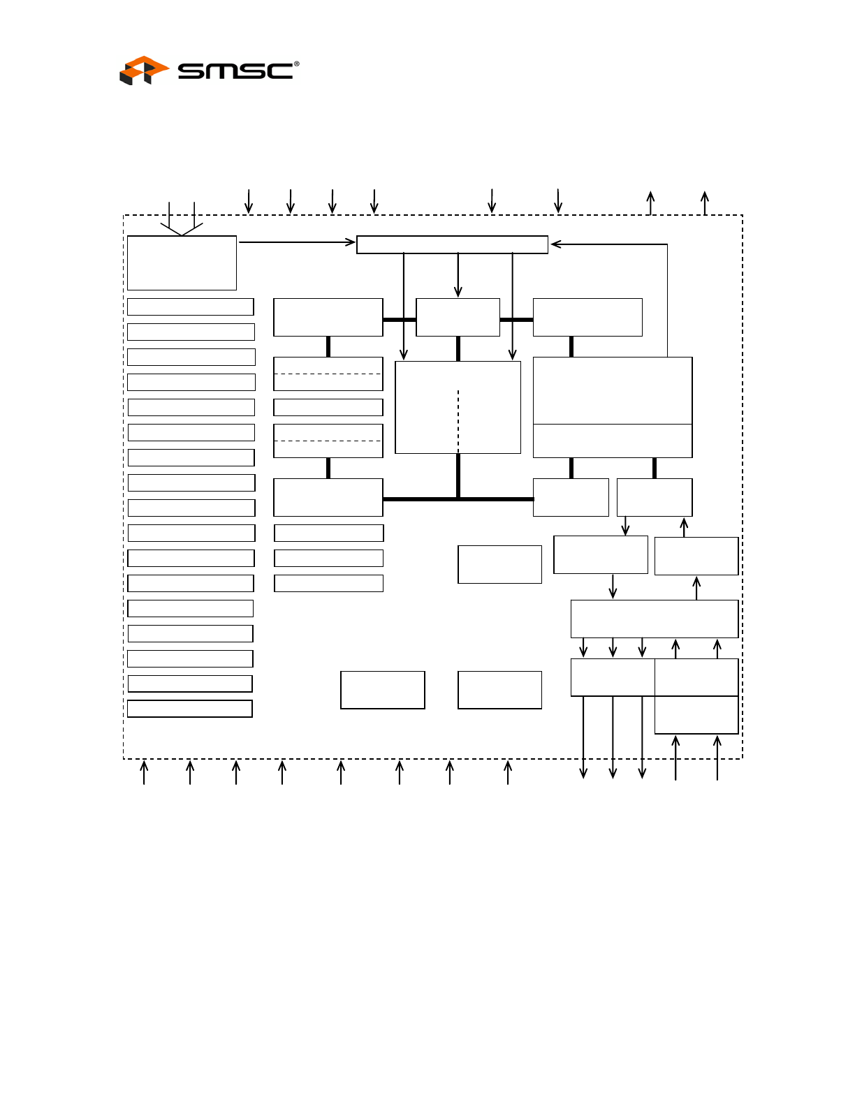
1.3
Internal Block Diagram
Mode Setting
Register Access
Control Circuit
Interrupt Status
Interrupt Mask
EC Command
Receive Mode(#01-#31)
Receive Flag(#01-#31)
Clock Master SID
Net. Standard Time
Alarm Setting
Receive SID
Search SID
MAX ID Setting (MAXID)
Node ID Setting (NID)
Page Size Setting (PS)
Data Rate Setting
Address pointer
Page Register
Address Register
Diag. Register
Data Register H
Data Register L
Data Latch
TENT-ID Register
CONFIG Register
SETUP Registers
Address
Multiplexer
Address Pointer
Data Latch
Shift Register
RX Synchro-
nous circuit
TX Signal
Generator
CMI Decode
CMI Encode
CMI Synchro
TXEN TXD
RXIN
Buffer Memory
512B 512B
Improved ARCNET Protocol
Micro Sequencer
Working Registers
Memory Access Mediation Circuit
RECON Timer
OSC
Reset Circuit
Micro-Controller bus
MAXID
NID
PS
CKP
nMUX nRWM W16 nSWAP
nSTALONE nDIAG
FLASHO
nNSTCOUT
TXEN2
RXIN2
3Port HUB Circuit
ERR-INFO
PIN-INFO
nHUBON nCMIBYP
Others
Clock
Figure 1 - TMC2074 Block Diagram
Dual Mode CircLink™ Controller
Datasheet
SMSC TMC2074
Page 9
Revision 0.2 (10-23-08)
DATASHEET
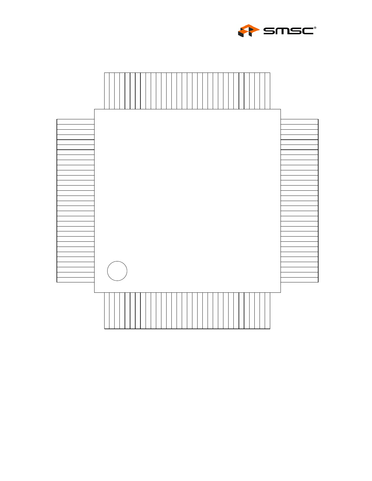
1.4 Pin
Configuration
*2
*2
*2 *3 *3 *1 *3
X
X
X
*2
X
X
*1
VSS
GP
IO7
/ P
O
15
GP
IO6
/ P
O
14
GP
IO5
/ P
O
13
GP
IO4
/ P
O
12
GP
IO3
/ P
O
11
VSS
GP
IO2
/ P
O
10
GP
IO1
/ P
O
9
GP
IO0
/ P
O
8
FL
A
S
H
O
nN
S
T
C
O
UT
VSS
X2
X1
VD
D
MCKI
N
NC
NC
NC
VSS
CK
P
2
CK
P
1
CK
P
0
NC
MAX
ID4
MAX
ID3
MAX
ID2
MAX
ID1
MAX
ID0
NC
VD
D
96 95 94 93 92 91 90 89 88 87 86 85 84 83 82 81 80 79 78 77 76 75 74 73 72 71 70 69 68 67 66 65
*1
VDD
97
64 VSS
*2
WPRE0 / SPRE0
98
63 NID4
WPRE1 / SPRE1
99
62 NID3
WPRE2 / SPRE2
100
61 NID2
X
NC
101
60 NID1
nTEST0
102
59 NID0
nTEST1
103
58 NC
X
nTEST2
104
57 PS1
nTEST3
105
56 PS0
(High) / NSTC0
106
55 NC
X
nEHRD / NSTC1
107
54 NSTPRE2
*2
VSS
108
53 NSTPRE1
nEHWR / NSTC2
109
52 NSTPRE0
(High) / NSTC3
110
51 nSTALONE
nCMIBYP
111
50 nDIAG
nOPMD
112
49 VDD
*1
*1
VDD
113
48 RXIN2
nHUBON
114
47 ET1
X
NC
115
46 RXIN
nMUX / SCM0
116
45 TXENPOL
nRWM / SCM1
117
44 VSS
*2
W16 / SCM2
118
43 TXEN2
nSWAP / SCM3
119
42 TXD
nCS / SCM4
120
41 TXEN
*2
VSS
121
40 nINTR / NSTUNLOC
X
NC
122
39 VSS
*2
X
NC
123
38 nRESET
*4
A0 / PO0 (nPOSTR)
124
37 NC
X
*1
VDD
125
36 NC
X
A1 /PO1
126
35 D15 / PI15
A2 (ALE) / PO2
127
34 D14 / PI14
*2
VSS
128
33 VDD
*1
1 2 3 4 5 6 7 8 9 10 11 12 13 14 15 16 17 18 19 20 21 22 23 24 25 26 27 28 29 30 31 32
VDD
A3 (ALEPO
L) /
PO
3
A
4 /
PO4
A
5 /
PO5
NC
NC
nD
SI
NV /
C
M
IE
RR
M
D
nR
D (n
DS) /
PO
6
nT
MO
DE
nW
R
(
D
IR
)
/ P
O
7
NC
VS
S
D0
(AD0) / P
I0 (nPI
ST
R)
D1
(AD1) / P
I1
D2
(AD2) / P
I2
D3
(AD3) / P
I3
VDD
D4
(AD4) / P
I4
D5
(AD5) / P
I5
VS
S
D
6 / P
I6
D
7 / P
I7
D
8 / P
I8
D
9 / P
I9
VDD
D1
0 / P
I10
D1
1 / P
I11
VS
S
D1
2 / P
I12
D1
3 / P
I13
NC
VS
S
*1
X
X
X
*2
*1
*2
*1
*2
X
*2
*1 Power supply (V
DD
)
*2 Power supply (Vss)
*3 Clock Signal
*4 Reset Signal
X
NC
Figure 2 - Pin Names: Pin Name in Peripheral Mode/Pin Name in Standalone Mode
Dual Mode CircLink™ Controller
Datasheet
Revision 0.2 (10-23-08)
Page 10
SMSC TMC2074
DATASHEET
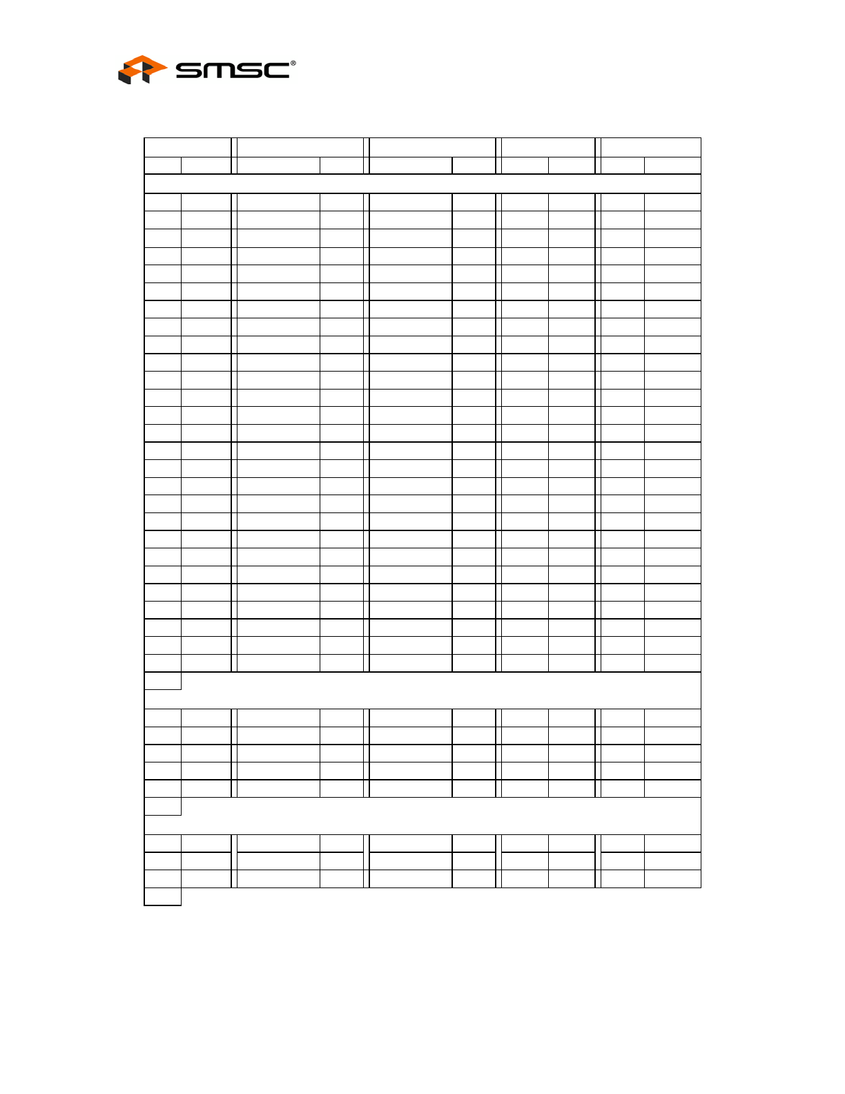
Table 1- Pin Lists Sorted by Function
Count
Pin NO.
Pin Name
Direction
Pin Name
Direction
Pull-Up
Type
Drive
Type
1
38
nRESET
IN
nRESET
IN
Internal
T-NRM
---
---
2
120
nCS
IN
SCM4
IN
Internal
T-NRM
---
---
3
124
A0
IN
PO0/nPOSTR
3s
/
O
Internal
T-NRM
4mA
4
126
A1
IN
PO1
3s.O
Internal
T-NRM
4mA
5
127
A2/ALE
IN
PO2
3s.O
Internal
T-NRM
4mA
6
2
A3/ALEPOL
IN
PO3
3s.O
Internal
T-NRM
4mA
7
3
A4
IN
PO4
3s.O
Internal
T-NRM
4mA
8
4
A5
IN
PO5
3s.O
Internal
T-NRM
4mA
9
8
nRD/nDS
IN
PO6
3s.O
Internal
T-NRM
4mA
10
10
nWR/DIR
IN
PO7
3s.O
Internal
T-NRM
4mA
11
13
D0/AD0
BI
PI0/nPISTR
IN
Internal
T-NRM
4mA
12
14
D1/AD1
BI
PI1
IN
Internal
T-NRM
4mA
13
15
D2/AD2
BI
PI2
IN
Internal
T-NRM
4mA
14
16
D3/AD3
BI
PI3
IN
Internal
T-NRM
4mA
15
18
D4/AD4
BI
PI4
IN
Internal
T-NRM
4mA
16
19
D5/AD5
BI
PI5
IN
Internal
T-NRM
4mA
17
21
D6
BI
PI6
IN
Internal
T-NRM
4mA
18
22
D7
BI
PI7
IN
Internal
T-NRM
4mA
19
23
D8
BI
PI8
IN
Internal
T-NRM
4mA
20
24
D9
BI
PI9
IN
Internal
T-NRM
4mA
21
26
D10
BI
PI10
IN
Internal
T-NRM
4mA
22
27
D11
BI
PI11
IN
Internal
T-NRM
4mA
23
29
D12
BI
PI12
IN
Internal
T-NRM
4mA
24
30
D13
BI
PI13
IN
Internal
T-NRM
4mA
25
34
D14
BI
PI14
IN
Internal
T-NRM
4mA
26
35
D15
BI
PI15
IN
Internal
T-NRM
4mA
27
40
nINTR
OUT NSTUNLOC OUT
---
---
4mA
Total:27
1
46
RXIN
IN
RXIN
IN
Internal
T-NRM
---
---
2
41
TXEN
OUT TXEN
OUT
---
---
4mA
3
42
TXD
OUT TXD
OUT
---
---
4mA
4
48
RXIN2
IN
RXIN2
IN
Internal
T-NRM
---
---
5
43
TXEN2
OUT TXEN2
OUT
---
---
4mA
Total:5
1
82
X1
IN
X1
IN
---
---
---
---
2
83
X2
OUT X2
OUT
---
---
---
---
3
80
MCKIN
IN
MCKIN
IN
Internal
T-NRM
---
---
Total:3
CPU Interface
Transceiver Interface
Clock
Peripheral Mode
Standalone Mode
Pin
Input Buffer
Output Buffer