

SMSC TMC2005-JT
Revision 1.1 (07-24-07)
DATASHEET
TMC2005-JT
ARCNET 5 Port HUB Controller
FEATURES
ARCNET HUB Circuit for ARCNET Protocol
(Data Rate From 156.25Kbps to 10Mbps)
Able to Connect Various Transceivers Directly
Device Includes TX/RX Timing Circuit for 5 Port
Hub and Direction Control Circuit, Jitter Correct
Circuit and Noise Cancel Circuit
Easy to Design 8 or 12 Port Hub
Can Connect with HYC9088 in Normal Mode
Can Connect with RS485 Transceiver,
HYC5000/4000/2000, Opt Module and TTL
Interface in Backplane Mode
Supports both Normal and Backplane Mode at
the Same Time for Media Conversion
+ 5V Single Power
GENERAL DESCRIPTION
When configuring a network, the maximum number of nodes and the maximum cable length are limited by the electric
capacity of the transceiver. In this case, the network is expanded by an equipment called a “HUB” or “repeater”. It
maybe necessary to have a converter between coax, T/P and the fiber cable. It is easy to design a HUB or a repeater
because the TMC2005 has various features for expanding such network.
It can connect with HYC9088, RS485 transceiver, HYC5000/4000/2000 and TTL interface for optical module. It can
connect with three different transceivers at the same time and convert the media of each. (The data rate cannot be
converted. It is necessary to operate all nodes in the same network at the same data rate). The Hubs can be
expanded by connecting two or more TMC2005 chips. By setting one of 5 ports to open-drain output, the Hub can be
expanded to either 12 or 16 ports.
ORDERING INFORMATION
Order Number(s):
TMC2005-JT for 64 pin, TQFP Lead-Free RoHS Compliant Package

ARCNET 5 Port HUB Controller
Datasheet
Revision 1.1 (07-24-07)
Page 2
SMSC TMC2005-JT
DATASHEET
80 ARKAY DRIVE, HAUPPAUGE, NY 11788 (631) 435-6000, FAX (631) 273-3123
Copyright © 2007 SMSC or its subsidiaries. All rights reserved.
Circuit diagrams and other information relating to SMSC products are included as a means of illustrating typical applications. Consequently, complete
information sufficient for construction purposes is not necessarily given. Although the information has been checked and is believed to be accurate, no
responsibility is assumed for inaccuracies. SMSC reserves the right to make changes to specifications and product descriptions at any time without
notice. Contact your local SMSC sales office to obtain the latest specifications before placing your product order. The provision of this information
does not convey to the purchaser of the described semiconductor devices any licenses under any patent rights or other intellectual property rights of
SMSC or others. All sales are expressly conditional on your agreement to the terms and conditions of the most recently dated version of SMSC's
standard Terms of Sale Agreement dated before the date of your order (the "Terms of Sale Agreement"). The product may contain design defects or
errors known as anomalies which may cause the product's functions to deviate from published specifications. Anomaly sheets are available upon
request. SMSC products are not designed, intended, authorized or warranted for use in any life support or other application where product failure
could cause or contribute to personal injury or severe property damage. Any and all such uses without prior written approval of an Officer of SMSC
and further testing and/or modification will be fully at the risk of the customer. Copies of this document or other SMSC literature, as well as the Terms
of Sale Agreement, may be obtained by visiting SMSC’s website at http://www.smsc.com. SMSC is a registered trademark of Standard Microsystems
Corporation (“SMSC”). Product names and company names are the trademarks of their respective holders.
SMSC DISCLAIMS AND EXCLUDES ANY AND ALL WARRANTIES, INCLUDING WITHOUT LIMITATION ANY AND ALL IMPLIED WARRANTIES
OF MERCHANTABILITY, FITNESS FOR A PARTICULAR PURPOSE, TITLE, AND AGAINST INFRINGEMENT AND THE LIKE, AND ANY AND
ALL WARRANTIES ARISING FROM ANY COURSE OF DEALING OR USAGE OF TRADE. IN NO EVENT SHALL SMSC BE LIABLE FOR ANY
DIRECT, INCIDENTAL, INDIRECT, SPECIAL, PUNITIVE, OR CONSEQUENTIAL DAMAGES; OR FOR LOST DATA, PROFITS, SAVINGS OR
REVENUES OF ANY KIND; REGARDLESS OF THE FORM OF ACTION, WHETHER BASED ON CONTRACT; TORT; NEGLIGENCE OF SMSC
OR OTHERS; STRICT LIABILITY; BREACH OF WARRANTY; OR OTHERWISE; WHETHER OR NOT ANY REMEDY OF BUYER IS HELD TO
HAVE FAILED OF ITS ESSENTIAL PURPOSE, AND WHETHER OR NOT SMSC HAS BEEN ADVISED OF THE POSSIBILITY OF SUCH
DAMAGES.

ARCNET 5 Port HUB Controller
Datasheet
SMSC TMC2005-JT
Page 3
Revision 1.1 (07-24-07)
DATASHEET
TABLE OF CONTENTS
FEATURES..................................................................................................................................................................1
GENERAL DESCRIPTION.......................................................................................................................................1
PIN CONFIGURATION ............................................................................................................................................4
BLOCK DIAGRAM....................................................................................................................................................4
BLOCK DIAGRAM....................................................................................................................................................5
DESCRIPTION OF PIN FUNCTIONS ....................................................................................................................5
DESCRIPTION OF PIN FUNCTIONS ....................................................................................................................6
TX/RX
I
NTERFACE
....................................................................................................................................................7
O
PERATING
M
ODE
S
ETUP
..........................................................................................................................................8
PLL ...........................................................................................................................................................................8
O
THER
S
IGNALS
........................................................................................................................................................9
OPERATIONAL DESCRIPTION...........................................................................................................................10
D
IRECTION
D
ETERMINATION
...................................................................................................................................10
D
IRECTION
R
ELEASE
...............................................................................................................................................10
J
ITTER
F
ILTER
..........................................................................................................................................................10
O
PTION
F
EATURE FOR
J
ITTER
F
ILTERING
.................................................................................................................11
O
PTION
F
EATURE FOR
N
OISE
C
UT MODE
.................................................................................................................11
APPLICATION
NOTES ........................................................................................................................................12
PORT GROUP...........................................................................................................................................................20
V
ARIOUS
S
ETUP
.......................................................................................................................................................20
E
XAMPLE
F
OR
O
PERATION
M
ODE
S
ETUP
T
O
E
ACH
P
ORT
........................................................................................20
N
OTE FOR
U
NUSED PORT
.........................................................................................................................................20
E
XAMPLE FOR
P
OWER
-O
N
R
ESET
C
IRCUIT
..............................................................................................................20
CONNECTING THE TMC2005 WITH INTERNAL PLL...................................................................................21
M
ETHOD
T
O
C
ONNECT
A
C
RYSTAL
C
LOCK
.............................................................................................................22
N
PLLTST
PIN
..........................................................................................................................................................22
CASCADING CONNECTION ................................................................................................................................23
R
ING
N
ETWORK
W
ITH THE
TMC2005.....................................................................................................................26
MAXIMUM
GUARANTEED
RATINGS*............................................................................................................27
STANDARD
OPERATING
CONDITION ............................................................................................................27
DC
CHARACTERISTIC
-
INPUT
PIN ..................................................................................................................27
DC
CHARACTERISTIC
-
OUTPUT
PIN ..............................................................................................................28
AC
CHARACTERISTIC
-
CLOCK
AND
RESET ...................................................................................................28
AC
CHARACTERISTIC
–
R
X WAVEFORMS AND
T
X WAVEFORMS
........................................................................29
TMC2005-JT 64 PIN TQFP PACKAGE OUTLINE .............................................................................................31
ARCNET 5 Port HUB Controller
Datasheet
Revision 1.1 (07-24-07)
Page 4
SMSC TMC2005-JT
DATASHEET
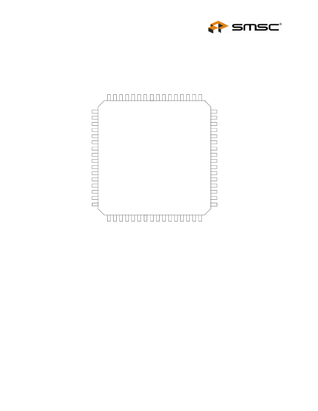
PIN CONFIGURATION
RX
IN
A
0
SA
TX
E
N
A
0
LA
MA
RX
IN
A
1
TX
E
N
A
1
VD
D
6
VSS
8
RX
IN
B
0
SB
TX
E
N
B
0
LB
MB
RX
IN
B
1
VS
S5
VS
S3
AV
SS
AGS
LP
AV
D
D
VD
D
3
VD
D
4
VS
S4
XT
LO
XT
L
I
VD
D
2
nPL
L
T
S
T
RX
FL
T
R0
VSS7
nPULSE1
nPULSE2
nP1BAK
VDD5
nCKOEN
nRST
VSS6
nBJA
nBJB
nBJE
nMBA
nMBB
nMBE
nEXTOD
TMC2005-JT
TXENB1
HM
SE
NC
LE
EXTRX
ME
VSS1
EXTTX
VDD1
CKO
VSS2
CKM2
CKM1
CKM0
1
2
3
4
5
6
7
8
9
10
11
12
13
14
15
46
17 18 19 20 21 22 23 24 25 26 27 28 29 30
47
48
33
34
35
36
37
38
39
40
41
42
43
44
45
64 63 62
49
50
51
52
53
54
55
56
57
58
59
60
NC
16
NC
31
NC
32
NC
61
ARCNET 5 Port HUB Controller
Datasheet
SMSC TMC2005-JT
Page 5
Revision 1.1 (07-24-07)
DATASHEET
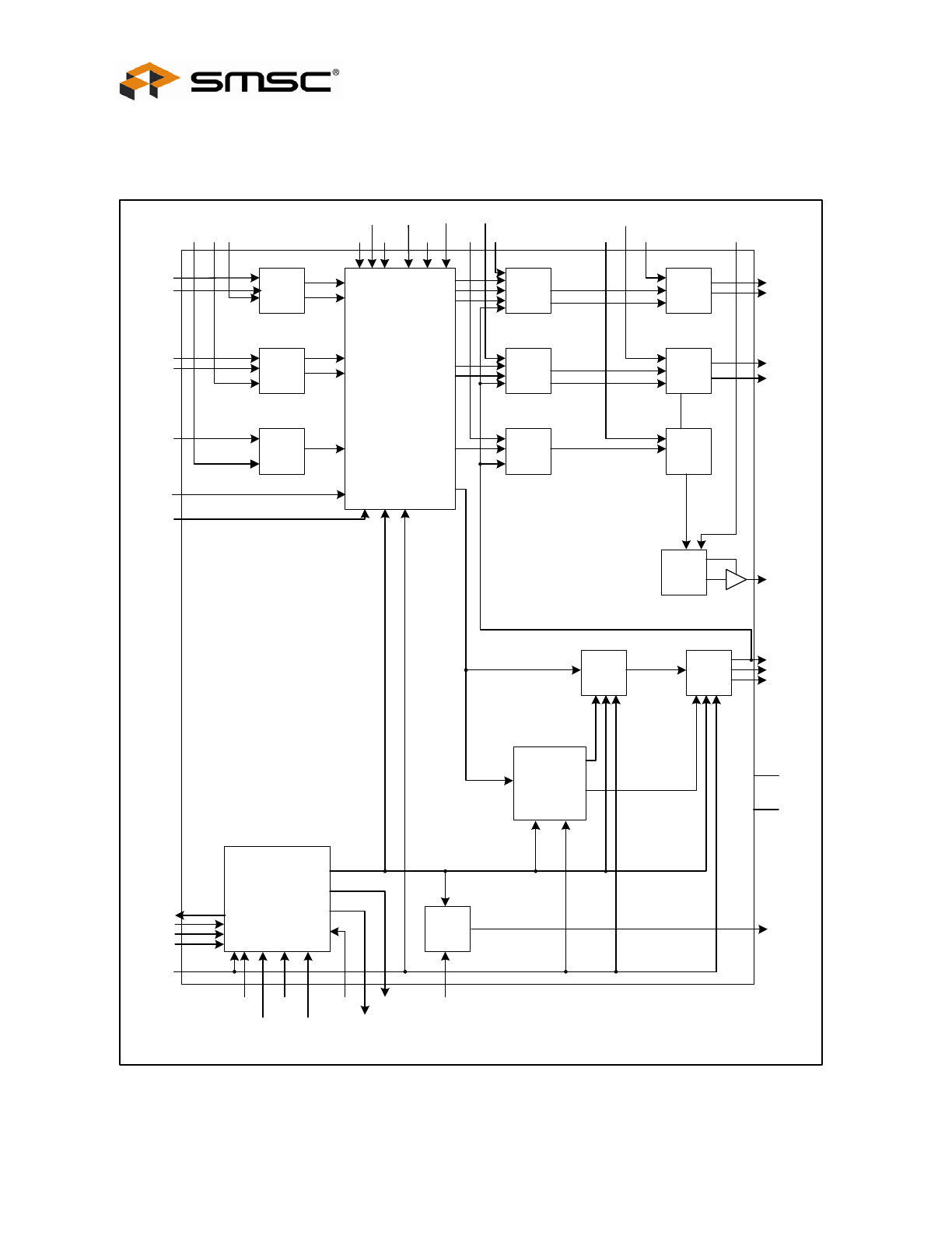
BLOCK DIAGRAM
Direction Control
Circuit
OR
Circuit
OR
Circuit
OR
Circuit
NOT
Circuit
NOT
Circuit
NOT
Circuit
NOT
Circuit
NOT
Circuit
NOT
Circuit
Rx
Buffer
Output
Control
Circuit
Tx
Pulse
Gen.
DPLL
AND
Circuit
Clock Multiplier
PLL
TXENA0
TXENA1
TXENB0
TXENB1
EXTTX
nP1BAK
nPULSE1
nPULSE2
VSS1- 8
VDD1- 6
CKO
nCKOEN
RO
LP
AVSS
nPLLTST
CKM2
CKM1
CKM0
nRST
AVSS
AVDD
XTLI
XTLO
RXFLT
EXTRX
RXINB1
RXINB0
RXINA1
RXINA0
SE SB SA
nBJE
nBJB
nBJA
nMBE
nMBB
nMBA
ME
MB
MA
LE
LB
LA
nEXTOD
HM

ARCNET 5 Port HUB Controller
Datasheet
Revision 1.1 (07-24-07)
Page 6
SMSC TMC2005-JT
DATASHEET
DESCRIPTION OF PIN FUNCTIONS
PIN NO.
NAME
INPUT/OUTPUT
DESCRIPTION
NOTE
1
TXENB1
OUTPUT
Port B-1 Tx output to media transceiver
2
HM
INPUT
Setting for traffic release time (It should
be open for normal operation.)
Pull-up
3
SE
INPUT
Port EXT. Polar assignment for EXTRX
input (0:active Hi, 1:active Low)
Pull-up
4
NC
Reserved. It should be open.
5
LE
INPUT
Port EXT. Polar assignment of EXTTX
output (0:active Low, 1:active Hi)
Pull-up
6
EXTRX
INPUT
Port EXT. RX-Data input from media
transceiver. Pull-up
7
ME
INPUT
Port EXT. Output mode assignment of
EXTTX (0:pulse output, 1:Tx control
output) Pull-up
8
VSS1
Ground
9
EXTTX
OUTPUT
Port EXT. Output to media transceiver.
10
VDD1
Power Supply
11
CKO
OUTPUT
Clock Output
12
VSS2
Ground
13
CKM2
INPUT
Network speed (data rate) setting.
Pull-up
14
CKM1
INPUT
Pull-up
15
CKM0
INPUT
Pull-up
16
NC
Reserved. It should be open.
17
RXFLT
INPUT
Test Pin. It should be open.
Pull-up
18
nPLLTST
INPUT
Test Pin for PLL.. It should connected to
VDD (Set to high)
19
VDD2
Power Supply
20
XTLI
INPUT
X'tal input/External clock input.
21
XTLO
OUTPUT
X'tal output
22
VSS4
Ground
23
NC
Reserved. It should be open.
24
VDD4
Power Supply
25
VDD3
Power Supply
26
AVDD
Analog Power Supply
27
RO
OUTPUT
VCO output for internal PLL.
28
LP
OUTPUT
Connection pin to loop filter for internal
PLL.
29
AGS
INPUT
Analog sense pin for internal PLL.
30
AVSS
Analog Ground
31
VSS3
Ground
32
VSS5
Ground
33
NC
Reserved. It should be open.
34
nEXTOD
INPUT
Port EXT. Open-drain mode (0:open-
drain output, 1:normal output)
Pull-up
35
nMBE
INPUT
Port EXT. Noise cut (0:on, 1:off)
Pull-up
36
nMBB
INPUT
Port A0/A1 Noise cut (0:on, 1:off)
Pull-up
37
nMBA
INPUT
Port B0/B1 Noise cut (0:on, 1:off)
Pull-up
38
nBJE
INPUT
Port EXT. Jitters correct mode (0:big
jitters mode, 1:normal mode)
Pull-up
39
nBJB
INPUT
Port A0/A1 Jitters correct mode (0:big
jitter mode, 1:normal mode)
Pull-up
40
nBJA
INPUT
Port B0/B1 Jitter correct mode (0:big
jitter mode, 1:normal mode)
Pull-up
41
VSS6
Ground
42
nRST
INPUT
Internal reset signal (active Low)
Pull-up
43
nCKOEN
INPUT
Enable of CKO output.
Pull-up

ARCNET 5 Port HUB Controller
Datasheet
SMSC TMC2005-JT
Page 7
Revision 1.1 (07-24-07)
DATASHEET
PIN NO.
NAME
INPUT/OUTPUT
DESCRIPTION
NOTE
44
VDD5
Power Supply.
45
nP1BAK
OUTPUT
nPULSE1 output (for backplane mode).
46
nPULSE2
OUTPUT
nPULSE2 output (for normal mode).
47
nPULSE1
OUTPUT
nPULSE1 output (for normal mode)
48
VSS7
Ground
49
RXINA0
INPUT
Port A-0 Rx-data input from media
transceiver. Pull-up
50
SA
INPUT
Port A. Polar assignment for RXINA0/A1
output (0:active Hi, 1:active Low)
Pull-up
51
TXENA0
OUTPUT
Port A-0 Tx output to media transceiver.
52
LA
INPUT
Port A. Polar assignment for TXENA0/A1
output (0:active Low, 1:active Hi)
Pull-up
53
RXINA1
INPUT
Port A-1 Rx-data input from media
transceiver. Pull-up
54
MA
INPUT
Port A. Mode assignment for
TXENA0/A1 (0:pulse output, 1:Tx control
output) Pull-up
55
TXENA1
OUTPUT
Port A-1 Tx output to media transceiver.
56
VDD6
Power Supply
57
NC
Reserved. It should be open.
58
VSS8
Ground
59
RXINB0
INPUT
Port B-0 Rx-data input from media
transceiver. Pull-up
60
SB
INPUT
Port B. Polar assignment for RXINA0/A1
input (0:active Hi, 1:Active Low)
Pull-up
61
TXENB0
OUTPUT
Port B-0 Tx output to media transceiver.
62
LB
INPUT
Port B. Polar assignment for TXENA0/A1
output (0:active Low, 1:active Hi)
Pull-up
63
RXINB1
INPUT
Port B-1 Rx-data input from media
transceiver. Pull-up
64
MB
INPUT
Port B. Mode assignment for
TXENA0/A1 (0:pulse output, 1:TX control
output) Pull-up
Note:
Pull-up: Input with a pull-up resistor 70KΩ ± 30%
TX/RX Interface
FEATURE NAME
INPUT/OUTPUT
DESCRIPTION
RX Port
RXINA [0:1]
RXINB [0:1]
EXTRX
INPUT
Setup the polarity by SA, SB, SE.
RX Port
Polar
Assignment
SA, SB, SE
INPUT
Setup the polarity of RXINA [0:1],
RXINB [0:1], EXTTX.
0 : active H
1: active L
TX Port
TX Control
TXENA [0:1]
TXENB [0:1]
EXTTX
OUTPUT
TX data pulse (Mx=0) or TX
enable signal (Mx=1).
Setup TX mode by MA, MB, ME.
Setup the polarity by LA, LB, LE
TX Port
TX Data
Output
nPULSE [1:2]
OUTPUT
TX pulse data into HYC9068S-
SK/9088S-SK when ARCNET
chip is at normal mode.
The pulse is always active Low.
TX Port
nP1BAK
OUTPUT
TX pulse data into RS485 driver
or HYC2485S/2488S when
ARCNET chip is at backplane

ARCNET 5 Port HUB Controller
Datasheet
Revision 1.1 (07-24-07)
Page 8
SMSC TMC2005-JT
DATASHEET
FEATURE NAME
INPUT/OUTPUT
DESCRIPTION
mode.
The pulse is always active Low.
TX Port
Polarity
Setup
LA, LB, LE
INPUT
Setup the polarity of TXENA
[0:1], TXENB [0:1], EXTTX.
0 : active L
1: active H
TX Port
Mode Setup
MA, MB, ME
INPUT
Setup the mode of TXENA [0:1],
TXENB [0:1], EXTTX.
0: Output TX pulse. (It is
equivalent to nTXEN “OR”
nP1BAK)
1: Output TX enable
Operating Mode Setup
FEATURE
NAME
INPUT/
OUTPUT
DESCRIPTION
Data rate
setup
CKM [0:2]
INPUT
Terminal to setup the data rate of TMC2005.
CKM2 CKM1 CKM0 DIVISOR MULTIPLIER SPEED
0 0 0 16 x1 156.25 Kbps
0 0 1 8 x1 312.5 Kbps
0 1 0 4 x1 625 Kbps
0 1 1 2 x1 1.25 Mbps
1 0 0 1 x1 2.5 Mbps
1 0 1 1 x2 5 Mbps
1 1 0 Reserved Reserved Reserved
1 1 1 1 x4 10 Mbps
External clock is 20MHz.
Refer to “VARIOUS SETUP”
Noise cut
mode
nMBA
nMBB
nMBE
INPUT
0: Cut off noise from received data
1: Don’t cut off noise
Setup “0” normally.
Big jitter
mode
nBJA
nBJB
nBJE
INPUT
Setup a jitter filter feature.
Select a pulse as reference phase used by DPLL.
0: 2
nd
pulse (big jitter mode)
1: 1
st
pulse (normal mode)
Open drain
mode
nEXTOD
INPUT
Setup a the use of EXTTX port.
0: Set EXTTX as open drain output and use as Ext.
1: Set EXTTX as normal output and use as 5
th
port.
PLL
FEATURE
NAME
INPUT/
OUTPUT
DESCRIPTION
LP
OUTPUT
Using PLL: Connect to an external condenser
“C1” for loop filter.
Using no PLL: must be open.
RO
OUTPUT
VCO
output
Using PLL: Connect to an external resistor “R0” for
loop filter.
Using no PLL: must be open.
AGS
INPUT
Analog sense input.
Using PLL: Connect to loop filter.
Using no PLL: Connect to ground.

ARCNET 5 Port HUB Controller
Datasheet
SMSC TMC2005-JT
Page 9
Revision 1.1 (07-24-07)
DATASHEET
FEATURE
NAME
INPUT/
OUTPUT
DESCRIPTION
nPLLTST
INPUT
Test pin for PLL.
Must always connect to VDD.
AVDD
Analog power supply
Using PLL: Analog power supply. There are some
limits on PCB pattern.
Using no PLL: Power supply (+5V) same as VDD1~6.
AVSS
Analog
ground
Using PLL: Analog ground. There are some limits on
PCB pattern.
Using no PLL: Use a ground same as VSS1~8.
Other Signals
FEATURES
NAME
INPUT/
OUTPUT
DESCRIPTION
CRYSTAL
INTERFACE
XTLI
INPUT
Connect a 20MHz crystal.
When supplying an external clock,
input the clock to this pin.
CRYSTAL
INTERFACE
XTLO
OUTPUT
Connect a 20MHz crystal.
When supplying an external clock, it
must be open.
SYSTEM RESET
INTERFACE
nRST
INPUT
Reset for initializing TMC2005. (active
Low)
TEST PIN
CKO
OUTPUT
Output internal clock of TMC2005.
TEST PIN
nCKOEN
INPUT
Output control of CKO.
0: Output internal clock on CKO.
1: Always output Low level on CKO.
Set “1” Normally.
TEST PIN
RXFLT
INPUT
It must be open
TEST PIN
NC [1:2]
It must be open
POWER SUPPLY
VDD [1:6]
Power supply (+5V)
GROUND VSS
[1:8]
Ground

ARCNET 5 Port HUB Controller
Datasheet
Revision 1.1 (07-24-07)
Page 10
SMSC TMC2005-JT
DATASHEET
OPERATIONAL DESCRIPTION
Direction Determination
All TX ports are set to disable mode in the initial state. When a signal is received from any RX ports, the circuit holds
the port on receiving mode (disable TX) and changes the other ports to sending mode (disable RX). One port stays in
RX and the rest change into TX after all. The circuit initializes the internal DPLL on the timing of received RX pulse,
and the RX buffer circuit stores the RX data and filters its jitter. TX controlling circuit regenerates the stored RX pulse
on nPULSE1, nPULSE2 and nP1BAK. The nPULSE1 and nPULSE2 are pulse output pins for transceivers
(HYC9088A) of ARCNET normal mode. The nP1BAK is a pulse output pin for transceiver (HYC5000/4000/2000 and
RS485 driver) of ARCNET back plane mode. When using optical transceiver, instead of these signals, TXENA [0:1],
TXENB [0:1], EXTTX (MA, MB, ME = 0) must be used as TX data inputs of the optical transceiver.
Direction Release
On ARCNET protocol, each TX message starts with 6-bits of “1” ALERT and each data byte is lead by three bits (1, 1,
0) preamble. To control the HUBs direction, the circuit monitors this bit pattern and holds the state. If the end of the bit
pattern comes, all TX ports return receiving mode (disable TX) again. The interval timer detects the end of the bit
pattern. During data is on line, silent period is less than 4 uS* because at least one bit “1” among 10-bits is received
while receiving the data. The minimum silent interval from the end of received data to the alert of the next data (the
minimum time of changing the direction) is the chip turn around time (12.6 uS*) of ARCNET controller. The interval
timer to detect the data end is set to 5.6uS by adding some margin to the above interval for neglecting the reflection
on a cable.
[Note] Numbers marked * are at 2.5Mbps operation.
Jitter Filter
To build a network with transceivers that introduce big jitter like ones for optical fiber, the old HUB that has direction
control only may cause a transmission error because jitters on each HUB are added when several HUBs were
connected in serial. The TMC2005 fixes that problem with jitter filtering and wave shaping through the following three
steps.
1) Input
Sampling
The TMC2005 samples a data on a network by eight times clock of the network data.
2) Jitter Filtering (DPLL)
The TMC2005 filters the jitter (± 100nS at 2.5Mbps) of network data sampled by 8X clock through the internal digital
PLL and stores the data into the buffer.
3) Wave Shaping Output
The TMC2005 re-synchronizes and regenerates the network data at the same clock as the data rate.
The capability of the jitter filtering is shown below.
DATA RATE
CAPABILITY OF JITTER FILTERING
10Mbps ±
25nS
5Mbps ±
50nS
2.5Mbps ±
100nS
1.25Mbps ±
200nS
625Kbps ±
400nS
312.5Kbps ±
800nS
156.25Kbps ±
1.6uS
SMSC TMC2005-JT
Revision 1.1 (07-24-07)
DATASHEET
TMC2005-JT
ARCNET 5 Port HUB Controller
FEATURES
ARCNET HUB Circuit for ARCNET Protocol
(Data Rate From 156.25Kbps to 10Mbps)
Able to Connect Various Transceivers Directly
Device Includes TX/RX Timing Circuit for 5 Port
Hub and Direction Control Circuit, Jitter Correct
Circuit and Noise Cancel Circuit
Easy to Design 8 or 12 Port Hub
Can Connect with HYC9088 in Normal Mode
Can Connect with RS485 Transceiver,
HYC5000/4000/2000, Opt Module and TTL
Interface in Backplane Mode
Supports both Normal and Backplane Mode at
the Same Time for Media Conversion
+ 5V Single Power
GENERAL DESCRIPTION
When configuring a network, the maximum number of nodes and the maximum cable length are limited by the electric
capacity of the transceiver. In this case, the network is expanded by an equipment called a “HUB” or “repeater”. It
maybe necessary to have a converter between coax, T/P and the fiber cable. It is easy to design a HUB or a repeater
because the TMC2005 has various features for expanding such network.
It can connect with HYC9088, RS485 transceiver, HYC5000/4000/2000 and TTL interface for optical module. It can
connect with three different transceivers at the same time and convert the media of each. (The data rate cannot be
converted. It is necessary to operate all nodes in the same network at the same data rate). The Hubs can be
expanded by connecting two or more TMC2005 chips. By setting one of 5 ports to open-drain output, the Hub can be
expanded to either 12 or 16 ports.
ORDERING INFORMATION
Order Number(s):
TMC2005-JT for 64 pin, TQFP Lead-Free RoHS Compliant Package
ARCNET 5 Port HUB Controller
Datasheet
Revision 1.1 (07-24-07)
Page 2
SMSC TMC2005-JT
DATASHEET
80 ARKAY DRIVE, HAUPPAUGE, NY 11788 (631) 435-6000, FAX (631) 273-3123
Copyright © 2007 SMSC or its subsidiaries. All rights reserved.
Circuit diagrams and other information relating to SMSC products are included as a means of illustrating typical applications. Consequently, complete
information sufficient for construction purposes is not necessarily given. Although the information has been checked and is believed to be accurate, no
responsibility is assumed for inaccuracies. SMSC reserves the right to make changes to specifications and product descriptions at any time without
notice. Contact your local SMSC sales office to obtain the latest specifications before placing your product order. The provision of this information
does not convey to the purchaser of the described semiconductor devices any licenses under any patent rights or other intellectual property rights of
SMSC or others. All sales are expressly conditional on your agreement to the terms and conditions of the most recently dated version of SMSC's
standard Terms of Sale Agreement dated before the date of your order (the "Terms of Sale Agreement"). The product may contain design defects or
errors known as anomalies which may cause the product's functions to deviate from published specifications. Anomaly sheets are available upon
request. SMSC products are not designed, intended, authorized or warranted for use in any life support or other application where product failure
could cause or contribute to personal injury or severe property damage. Any and all such uses without prior written approval of an Officer of SMSC
and further testing and/or modification will be fully at the risk of the customer. Copies of this document or other SMSC literature, as well as the Terms
of Sale Agreement, may be obtained by visiting SMSC’s website at http://www.smsc.com. SMSC is a registered trademark of Standard Microsystems
Corporation (“SMSC”). Product names and company names are the trademarks of their respective holders.
SMSC DISCLAIMS AND EXCLUDES ANY AND ALL WARRANTIES, INCLUDING WITHOUT LIMITATION ANY AND ALL IMPLIED WARRANTIES
OF MERCHANTABILITY, FITNESS FOR A PARTICULAR PURPOSE, TITLE, AND AGAINST INFRINGEMENT AND THE LIKE, AND ANY AND
ALL WARRANTIES ARISING FROM ANY COURSE OF DEALING OR USAGE OF TRADE. IN NO EVENT SHALL SMSC BE LIABLE FOR ANY
DIRECT, INCIDENTAL, INDIRECT, SPECIAL, PUNITIVE, OR CONSEQUENTIAL DAMAGES; OR FOR LOST DATA, PROFITS, SAVINGS OR
REVENUES OF ANY KIND; REGARDLESS OF THE FORM OF ACTION, WHETHER BASED ON CONTRACT; TORT; NEGLIGENCE OF SMSC
OR OTHERS; STRICT LIABILITY; BREACH OF WARRANTY; OR OTHERWISE; WHETHER OR NOT ANY REMEDY OF BUYER IS HELD TO
HAVE FAILED OF ITS ESSENTIAL PURPOSE, AND WHETHER OR NOT SMSC HAS BEEN ADVISED OF THE POSSIBILITY OF SUCH
DAMAGES.
ARCNET 5 Port HUB Controller
Datasheet
SMSC TMC2005-JT
Page 3
Revision 1.1 (07-24-07)
DATASHEET
TABLE OF CONTENTS
FEATURES..................................................................................................................................................................1
GENERAL DESCRIPTION.......................................................................................................................................1
PIN CONFIGURATION ............................................................................................................................................4
BLOCK DIAGRAM....................................................................................................................................................4
BLOCK DIAGRAM....................................................................................................................................................5
DESCRIPTION OF PIN FUNCTIONS ....................................................................................................................5
DESCRIPTION OF PIN FUNCTIONS ....................................................................................................................6
TX/RX
I
NTERFACE
....................................................................................................................................................7
O
PERATING
M
ODE
S
ETUP
..........................................................................................................................................8
PLL ...........................................................................................................................................................................8
O
THER
S
IGNALS
........................................................................................................................................................9
OPERATIONAL DESCRIPTION...........................................................................................................................10
D
IRECTION
D
ETERMINATION
...................................................................................................................................10
D
IRECTION
R
ELEASE
...............................................................................................................................................10
J
ITTER
F
ILTER
..........................................................................................................................................................10
O
PTION
F
EATURE FOR
J
ITTER
F
ILTERING
.................................................................................................................11
O
PTION
F
EATURE FOR
N
OISE
C
UT MODE
.................................................................................................................11
APPLICATION
NOTES ........................................................................................................................................12
PORT GROUP...........................................................................................................................................................20
V
ARIOUS
S
ETUP
.......................................................................................................................................................20
E
XAMPLE
F
OR
O
PERATION
M
ODE
S
ETUP
T
O
E
ACH
P
ORT
........................................................................................20
N
OTE FOR
U
NUSED PORT
.........................................................................................................................................20
E
XAMPLE FOR
P
OWER
-O
N
R
ESET
C
IRCUIT
..............................................................................................................20
CONNECTING THE TMC2005 WITH INTERNAL PLL...................................................................................21
M
ETHOD
T
O
C
ONNECT
A
C
RYSTAL
C
LOCK
.............................................................................................................22
N
PLLTST
PIN
..........................................................................................................................................................22
CASCADING CONNECTION ................................................................................................................................23
R
ING
N
ETWORK
W
ITH THE
TMC2005.....................................................................................................................26
MAXIMUM
GUARANTEED
RATINGS*............................................................................................................27
STANDARD
OPERATING
CONDITION ............................................................................................................27
DC
CHARACTERISTIC
-
INPUT
PIN ..................................................................................................................27
DC
CHARACTERISTIC
-
OUTPUT
PIN ..............................................................................................................28
AC
CHARACTERISTIC
-
CLOCK
AND
RESET ...................................................................................................28
AC
CHARACTERISTIC
–
R
X WAVEFORMS AND
T
X WAVEFORMS
........................................................................29
TMC2005-JT 64 PIN TQFP PACKAGE OUTLINE .............................................................................................31
ARCNET 5 Port HUB Controller
Datasheet
Revision 1.1 (07-24-07)
Page 4
SMSC TMC2005-JT
DATASHEET
PIN CONFIGURATION
RX
IN
A
0
SA
TX
E
N
A
0
LA
MA
RX
IN
A
1
TX
E
N
A
1
VD
D
6
VSS
8
RX
IN
B
0
SB
TX
E
N
B
0
LB
MB
RX
IN
B
1
VS
S5
VS
S3
AV
SS
AGS
LP
AV
D
D
VD
D
3
VD
D
4
VS
S4
XT
LO
XT
L
I
VD
D
2
nPL
L
T
S
T
RX
FL
T
R0
VSS7
nPULSE1
nPULSE2
nP1BAK
VDD5
nCKOEN
nRST
VSS6
nBJA
nBJB
nBJE
nMBA
nMBB
nMBE
nEXTOD
TMC2005-JT
TXENB1
HM
SE
NC
LE
EXTRX
ME
VSS1
EXTTX
VDD1
CKO
VSS2
CKM2
CKM1
CKM0
1
2
3
4
5
6
7
8
9
10
11
12
13
14
15
46
17 18 19 20 21 22 23 24 25 26 27 28 29 30
47
48
33
34
35
36
37
38
39
40
41
42
43
44
45
64 63 62
49
50
51
52
53
54
55
56
57
58
59
60
NC
16
NC
31
NC
32
NC
61
ARCNET 5 Port HUB Controller
Datasheet
SMSC TMC2005-JT
Page 5
Revision 1.1 (07-24-07)
DATASHEET
BLOCK DIAGRAM
Direction Control
Circuit
OR
Circuit
OR
Circuit
OR
Circuit
NOT
Circuit
NOT
Circuit
NOT
Circuit
NOT
Circuit
NOT
Circuit
NOT
Circuit
Rx
Buffer
Output
Control
Circuit
Tx
Pulse
Gen.
DPLL
AND
Circuit
Clock Multiplier
PLL
TXENA0
TXENA1
TXENB0
TXENB1
EXTTX
nP1BAK
nPULSE1
nPULSE2
VSS1- 8
VDD1- 6
CKO
nCKOEN
RO
LP
AVSS
nPLLTST
CKM2
CKM1
CKM0
nRST
AVSS
AVDD
XTLI
XTLO
RXFLT
EXTRX
RXINB1
RXINB0
RXINA1
RXINA0
SE SB SA
nBJE
nBJB
nBJA
nMBE
nMBB
nMBA
ME
MB
MA
LE
LB
LA
nEXTOD
HM
ARCNET 5 Port HUB Controller
Datasheet
Revision 1.1 (07-24-07)
Page 6
SMSC TMC2005-JT
DATASHEET
DESCRIPTION OF PIN FUNCTIONS
PIN NO.
NAME
INPUT/OUTPUT
DESCRIPTION
NOTE
1
TXENB1
OUTPUT
Port B-1 Tx output to media transceiver
2
HM
INPUT
Setting for traffic release time (It should
be open for normal operation.)
Pull-up
3
SE
INPUT
Port EXT. Polar assignment for EXTRX
input (0:active Hi, 1:active Low)
Pull-up
4
NC
Reserved. It should be open.
5
LE
INPUT
Port EXT. Polar assignment of EXTTX
output (0:active Low, 1:active Hi)
Pull-up
6
EXTRX
INPUT
Port EXT. RX-Data input from media
transceiver. Pull-up
7
ME
INPUT
Port EXT. Output mode assignment of
EXTTX (0:pulse output, 1:Tx control
output) Pull-up
8
VSS1
Ground
9
EXTTX
OUTPUT
Port EXT. Output to media transceiver.
10
VDD1
Power Supply
11
CKO
OUTPUT
Clock Output
12
VSS2
Ground
13
CKM2
INPUT
Network speed (data rate) setting.
Pull-up
14
CKM1
INPUT
Pull-up
15
CKM0
INPUT
Pull-up
16
NC
Reserved. It should be open.
17
RXFLT
INPUT
Test Pin. It should be open.
Pull-up
18
nPLLTST
INPUT
Test Pin for PLL.. It should connected to
VDD (Set to high)
19
VDD2
Power Supply
20
XTLI
INPUT
X'tal input/External clock input.
21
XTLO
OUTPUT
X'tal output
22
VSS4
Ground
23
NC
Reserved. It should be open.
24
VDD4
Power Supply
25
VDD3
Power Supply
26
AVDD
Analog Power Supply
27
RO
OUTPUT
VCO output for internal PLL.
28
LP
OUTPUT
Connection pin to loop filter for internal
PLL.
29
AGS
INPUT
Analog sense pin for internal PLL.
30
AVSS
Analog Ground
31
VSS3
Ground
32
VSS5
Ground
33
NC
Reserved. It should be open.
34
nEXTOD
INPUT
Port EXT. Open-drain mode (0:open-
drain output, 1:normal output)
Pull-up
35
nMBE
INPUT
Port EXT. Noise cut (0:on, 1:off)
Pull-up
36
nMBB
INPUT
Port A0/A1 Noise cut (0:on, 1:off)
Pull-up
37
nMBA
INPUT
Port B0/B1 Noise cut (0:on, 1:off)
Pull-up
38
nBJE
INPUT
Port EXT. Jitters correct mode (0:big
jitters mode, 1:normal mode)
Pull-up
39
nBJB
INPUT
Port A0/A1 Jitters correct mode (0:big
jitter mode, 1:normal mode)
Pull-up
40
nBJA
INPUT
Port B0/B1 Jitter correct mode (0:big
jitter mode, 1:normal mode)
Pull-up
41
VSS6
Ground
42
nRST
INPUT
Internal reset signal (active Low)
Pull-up
43
nCKOEN
INPUT
Enable of CKO output.
Pull-up
ARCNET 5 Port HUB Controller
Datasheet
SMSC TMC2005-JT
Page 7
Revision 1.1 (07-24-07)
DATASHEET
PIN NO.
NAME
INPUT/OUTPUT
DESCRIPTION
NOTE
44
VDD5
Power Supply.
45
nP1BAK
OUTPUT
nPULSE1 output (for backplane mode).
46
nPULSE2
OUTPUT
nPULSE2 output (for normal mode).
47
nPULSE1
OUTPUT
nPULSE1 output (for normal mode)
48
VSS7
Ground
49
RXINA0
INPUT
Port A-0 Rx-data input from media
transceiver. Pull-up
50
SA
INPUT
Port A. Polar assignment for RXINA0/A1
output (0:active Hi, 1:active Low)
Pull-up
51
TXENA0
OUTPUT
Port A-0 Tx output to media transceiver.
52
LA
INPUT
Port A. Polar assignment for TXENA0/A1
output (0:active Low, 1:active Hi)
Pull-up
53
RXINA1
INPUT
Port A-1 Rx-data input from media
transceiver. Pull-up
54
MA
INPUT
Port A. Mode assignment for
TXENA0/A1 (0:pulse output, 1:Tx control
output) Pull-up
55
TXENA1
OUTPUT
Port A-1 Tx output to media transceiver.
56
VDD6
Power Supply
57
NC
Reserved. It should be open.
58
VSS8
Ground
59
RXINB0
INPUT
Port B-0 Rx-data input from media
transceiver. Pull-up
60
SB
INPUT
Port B. Polar assignment for RXINA0/A1
input (0:active Hi, 1:Active Low)
Pull-up
61
TXENB0
OUTPUT
Port B-0 Tx output to media transceiver.
62
LB
INPUT
Port B. Polar assignment for TXENA0/A1
output (0:active Low, 1:active Hi)
Pull-up
63
RXINB1
INPUT
Port B-1 Rx-data input from media
transceiver. Pull-up
64
MB
INPUT
Port B. Mode assignment for
TXENA0/A1 (0:pulse output, 1:TX control
output) Pull-up
Note:
Pull-up: Input with a pull-up resistor 70KΩ ± 30%
TX/RX Interface
FEATURE NAME
INPUT/OUTPUT
DESCRIPTION
RX Port
RXINA [0:1]
RXINB [0:1]
EXTRX
INPUT
Setup the polarity by SA, SB, SE.
RX Port
Polar
Assignment
SA, SB, SE
INPUT
Setup the polarity of RXINA [0:1],
RXINB [0:1], EXTTX.
0 : active H
1: active L
TX Port
TX Control
TXENA [0:1]
TXENB [0:1]
EXTTX
OUTPUT
TX data pulse (Mx=0) or TX
enable signal (Mx=1).
Setup TX mode by MA, MB, ME.
Setup the polarity by LA, LB, LE
TX Port
TX Data
Output
nPULSE [1:2]
OUTPUT
TX pulse data into HYC9068S-
SK/9088S-SK when ARCNET
chip is at normal mode.
The pulse is always active Low.
TX Port
nP1BAK
OUTPUT
TX pulse data into RS485 driver
or HYC2485S/2488S when
ARCNET chip is at backplane
ARCNET 5 Port HUB Controller
Datasheet
Revision 1.1 (07-24-07)
Page 8
SMSC TMC2005-JT
DATASHEET
FEATURE NAME
INPUT/OUTPUT
DESCRIPTION
mode.
The pulse is always active Low.
TX Port
Polarity
Setup
LA, LB, LE
INPUT
Setup the polarity of TXENA
[0:1], TXENB [0:1], EXTTX.
0 : active L
1: active H
TX Port
Mode Setup
MA, MB, ME
INPUT
Setup the mode of TXENA [0:1],
TXENB [0:1], EXTTX.
0: Output TX pulse. (It is
equivalent to nTXEN “OR”
nP1BAK)
1: Output TX enable
Operating Mode Setup
FEATURE
NAME
INPUT/
OUTPUT
DESCRIPTION
Data rate
setup
CKM [0:2]
INPUT
Terminal to setup the data rate of TMC2005.
CKM2 CKM1 CKM0 DIVISOR MULTIPLIER SPEED
0 0 0 16 x1 156.25 Kbps
0 0 1 8 x1 312.5 Kbps
0 1 0 4 x1 625 Kbps
0 1 1 2 x1 1.25 Mbps
1 0 0 1 x1 2.5 Mbps
1 0 1 1 x2 5 Mbps
1 1 0 Reserved Reserved Reserved
1 1 1 1 x4 10 Mbps
External clock is 20MHz.
Refer to “VARIOUS SETUP”
Noise cut
mode
nMBA
nMBB
nMBE
INPUT
0: Cut off noise from received data
1: Don’t cut off noise
Setup “0” normally.
Big jitter
mode
nBJA
nBJB
nBJE
INPUT
Setup a jitter filter feature.
Select a pulse as reference phase used by DPLL.
0: 2
nd
pulse (big jitter mode)
1: 1
st
pulse (normal mode)
Open drain
mode
nEXTOD
INPUT
Setup a the use of EXTTX port.
0: Set EXTTX as open drain output and use as Ext.
1: Set EXTTX as normal output and use as 5
th
port.
PLL
FEATURE
NAME
INPUT/
OUTPUT
DESCRIPTION
LP
OUTPUT
Using PLL: Connect to an external condenser
“C1” for loop filter.
Using no PLL: must be open.
RO
OUTPUT
VCO
output
Using PLL: Connect to an external resistor “R0” for
loop filter.
Using no PLL: must be open.
AGS
INPUT
Analog sense input.
Using PLL: Connect to loop filter.
Using no PLL: Connect to ground.
ARCNET 5 Port HUB Controller
Datasheet
SMSC TMC2005-JT
Page 9
Revision 1.1 (07-24-07)
DATASHEET
FEATURE
NAME
INPUT/
OUTPUT
DESCRIPTION
nPLLTST
INPUT
Test pin for PLL.
Must always connect to VDD.
AVDD
Analog power supply
Using PLL: Analog power supply. There are some
limits on PCB pattern.
Using no PLL: Power supply (+5V) same as VDD1~6.
AVSS
Analog
ground
Using PLL: Analog ground. There are some limits on
PCB pattern.
Using no PLL: Use a ground same as VSS1~8.
Other Signals
FEATURES
NAME
INPUT/
OUTPUT
DESCRIPTION
CRYSTAL
INTERFACE
XTLI
INPUT
Connect a 20MHz crystal.
When supplying an external clock,
input the clock to this pin.
CRYSTAL
INTERFACE
XTLO
OUTPUT
Connect a 20MHz crystal.
When supplying an external clock, it
must be open.
SYSTEM RESET
INTERFACE
nRST
INPUT
Reset for initializing TMC2005. (active
Low)
TEST PIN
CKO
OUTPUT
Output internal clock of TMC2005.
TEST PIN
nCKOEN
INPUT
Output control of CKO.
0: Output internal clock on CKO.
1: Always output Low level on CKO.
Set “1” Normally.
TEST PIN
RXFLT
INPUT
It must be open
TEST PIN
NC [1:2]
It must be open
POWER SUPPLY
VDD [1:6]
Power supply (+5V)
GROUND VSS
[1:8]
Ground
ARCNET 5 Port HUB Controller
Datasheet
Revision 1.1 (07-24-07)
Page 10
SMSC TMC2005-JT
DATASHEET
OPERATIONAL DESCRIPTION
Direction Determination
All TX ports are set to disable mode in the initial state. When a signal is received from any RX ports, the circuit holds
the port on receiving mode (disable TX) and changes the other ports to sending mode (disable RX). One port stays in
RX and the rest change into TX after all. The circuit initializes the internal DPLL on the timing of received RX pulse,
and the RX buffer circuit stores the RX data and filters its jitter. TX controlling circuit regenerates the stored RX pulse
on nPULSE1, nPULSE2 and nP1BAK. The nPULSE1 and nPULSE2 are pulse output pins for transceivers
(HYC9088A) of ARCNET normal mode. The nP1BAK is a pulse output pin for transceiver (HYC5000/4000/2000 and
RS485 driver) of ARCNET back plane mode. When using optical transceiver, instead of these signals, TXENA [0:1],
TXENB [0:1], EXTTX (MA, MB, ME = 0) must be used as TX data inputs of the optical transceiver.
Direction Release
On ARCNET protocol, each TX message starts with 6-bits of “1” ALERT and each data byte is lead by three bits (1, 1,
0) preamble. To control the HUBs direction, the circuit monitors this bit pattern and holds the state. If the end of the bit
pattern comes, all TX ports return receiving mode (disable TX) again. The interval timer detects the end of the bit
pattern. During data is on line, silent period is less than 4 uS* because at least one bit “1” among 10-bits is received
while receiving the data. The minimum silent interval from the end of received data to the alert of the next data (the
minimum time of changing the direction) is the chip turn around time (12.6 uS*) of ARCNET controller. The interval
timer to detect the data end is set to 5.6uS by adding some margin to the above interval for neglecting the reflection
on a cable.
[Note] Numbers marked * are at 2.5Mbps operation.
Jitter Filter
To build a network with transceivers that introduce big jitter like ones for optical fiber, the old HUB that has direction
control only may cause a transmission error because jitters on each HUB are added when several HUBs were
connected in serial. The TMC2005 fixes that problem with jitter filtering and wave shaping through the following three
steps.
1) Input
Sampling
The TMC2005 samples a data on a network by eight times clock of the network data.
2) Jitter Filtering (DPLL)
The TMC2005 filters the jitter (± 100nS at 2.5Mbps) of network data sampled by 8X clock through the internal digital
PLL and stores the data into the buffer.
3) Wave Shaping Output
The TMC2005 re-synchronizes and regenerates the network data at the same clock as the data rate.
The capability of the jitter filtering is shown below.
DATA RATE
CAPABILITY OF JITTER FILTERING
10Mbps ±
25nS
5Mbps ±
50nS
2.5Mbps ±
100nS
1.25Mbps ±
200nS
625Kbps ±
400nS
312.5Kbps ±
800nS
156.25Kbps ±
1.6uS