
2007-2014 Microchip Technology Inc.
DS20002052D-page 1
MCP1401/02
Features
• High Peak Output Current: 500 mA (typical)
• Wide Input Supply Voltage Operating Range:
- 4.5V to 18V
• Low Shoot-Through/Cross-Conduction Current in
Output Stage
• High Capacitive Load Drive Capability:
- 470 pF in 19 ns (typical)
- 1000 pF in 34 ns (typical)
• Short Delay Times: 35 ns (typical)
• Matched Rise/Fall Times
• Low Supply Current:
- With Logic ‘1’ Input – 0.85 mA (typical)
- With Logic ‘0’ Input – 0.1 mA (typical)
• Latch-Up Protected: Will Withstand 500 mA
Reverse Current
• Logic Input Will Withstand Negative Swing up to 5V
• Space-Saving 5-Lead SOT-23 Package
Applications
• Switch Mode Power Supplies
• Pulse Transformer Drive
• Line Drivers
• Motor and Solenoid Drive
General Description
The MCP1401/02 are high-speed MOSFET drivers
capable of providing 500 mA of peak current. The
inverting or non-inverting single channel output is
directly controlled from either TTL or CMOS (3V to
18V). These devices also feature low shoot-through
current, matched rise/fall times and propagation delays
which make them ideal for high switching frequency
applications.
The MCP1401/02 devices operate from a single 4.5V
to 18V power supply and can easily charge and
discharge 470 pF gate capacitance in under 19 ns
(typical). They provide low enough impedances in both
the On and Off states to ensure the MOSFET’s
intended state will not be affected, even by large
transients.
These devices are highly latch-up resistant under any
conditions within their power and voltage ratings. They
are not subject to damage when up to 5V of noise
spiking (of either polarity) occurs on the Ground pin.
They can accept, without damage or logic upset, up to
500 mA of reverse current being forced back into their
outputs. All terminals are fully protected against
Electrostatic Discharge (ESD) up to 1 kV (HBM) and
300V (MM).
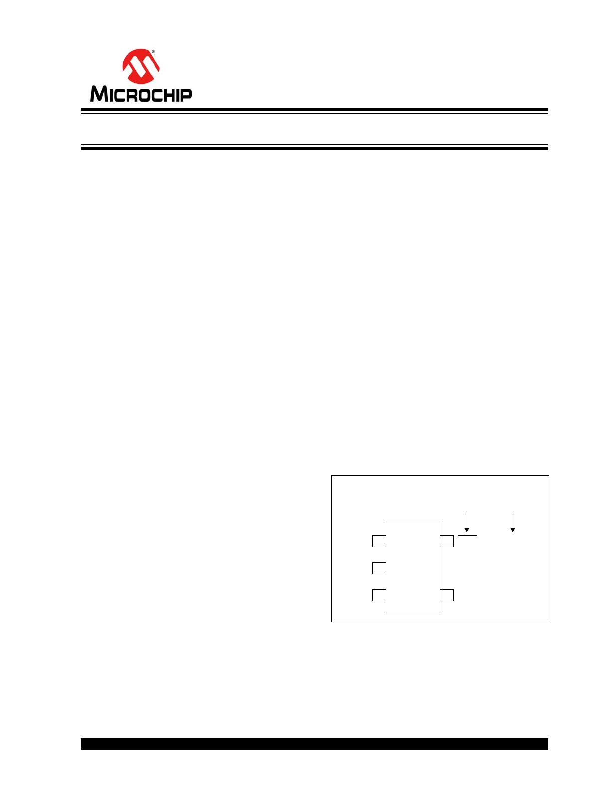
Package Types
4
1
2
3
5
V
DD
GND
IN
OUT
GND
OUT
GND
MCP1401 MCP1402
SOT-23
Tiny 500 mA, High-Speed Power MOSFET Driver
MCP1401/02
DS20002052D-page 2
2007-2014 Microchip Technology Inc.
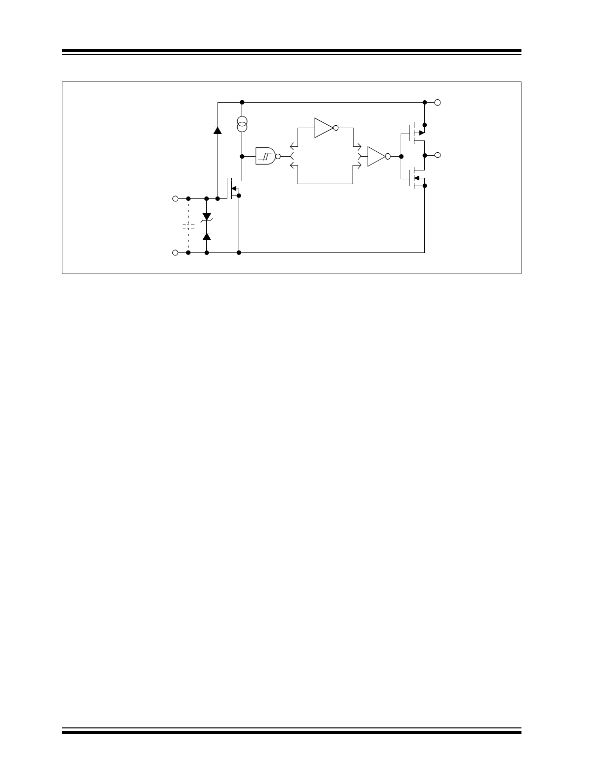
Functional Block Diagram
Effective
Input C = 25 pF
MCP1401 Inverting
MCP1402 Non-inverting
Input
GND
V
DD
300 mV
4.7V
Inverting
Non-inverting
850 µA
Output
(Each Input)
2007-2014 Microchip Technology Inc.
DS20002052D-page 3
MCP1401/02
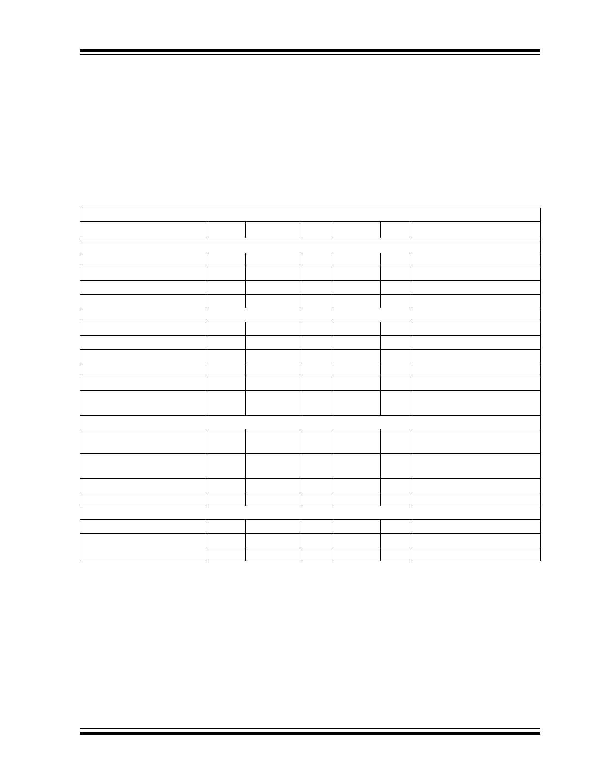
1.0
ELECTRICAL
CHARACTERISTICS
Absolute Maximum Ratings†
Supply Voltage ..................................................... +20V
Input Voltage .................... (V
DD
+ 0.3V) to (GND – 5V)
Input Current (V
IN
> V
DD
) ................................... 50 mA
Package Power Dissipation (T
A
= 50
o
C)
SOT-23-5 ........................................................ 0.39W
† Notice: Stresses above those listed under “Maximum
Ratings” may cause permanent damage to the device.
This is a stress rating only and functional operation of
the device at those or any other conditions above those
indicated in the operational sections of this
specification is not intended. Exposure to maximum
rating conditions for extended periods may affect
device reliability.
DC CHARACTERISTICS (
Note 2
)
Electrical Specifications: Unless otherwise indicated, T
A
= +25°C, with 4.5V
V
DD
18V.
Parameters
Sym.
Min.
Typ.
Max.
Units
Conditions
Input
Logic ‘1’, High Input Voltage
V
IH
2.4
1.5
—
V
Logic ‘0’, Low Input Voltage
V
IL
—
1.3
0.8
V
Input Current
I
IN
-1
—
1
µA
0V
V
IN
V
DD
Input Voltage
V
IN
-5
—
V
DD
+ 0.3
V
Output
High Output Voltage
V
OH
V
DD
– 0.025
—
—
V
DC Test
Low Output Voltage
V
OL
—
—
0.025
V
DC Test
Output Resistance, High
R
OH
—
12
18
I
OUT
= 10 mA, V
DD
= 18V
Output Resistance, Low
R
OL
—
10
16
I
OUT
= 10 mA, V
DD
= 18V
Peak Output Current
I
PK
—
0.5
—
A
V
DD
18V (
Note 2
)
Latch-Up Protection
Withstand Reverse Current
I
REV
—
> 0.5
—
A
Duty cycle
2%, t 300 µs
Switching Time (
Note 1
)
Rise Time
t
R
—
19
25
ns
Figure 4-1
,
Figure 4-2
C
L
= 470 pF
Fall Time
t
F
—
15
20
ns
Figure 4-1
,
Figure 4-2
C
L
= 470 pF
Delay Time
t
D1
—
35
40
ns
Figure 4-1
,
Figure 4-2
Delay Time
t
D2
—
35
40
ns
Figure 4-1
,
Figure 4-2
Power Supply
Supply Voltage
V
DD
4.5
—
18.0
V
Power Supply Current
I
S
—
0.85
1.1
mA
V
IN
= 3V
I
S
—
0.10
0.20
mA
V
IN
= 0V
Note 1:
Switching times ensured by design.
2:
Tested during characterization, not production tested.
MCP1401/02
DS20002052D-page 4
2007-2014 Microchip Technology Inc.
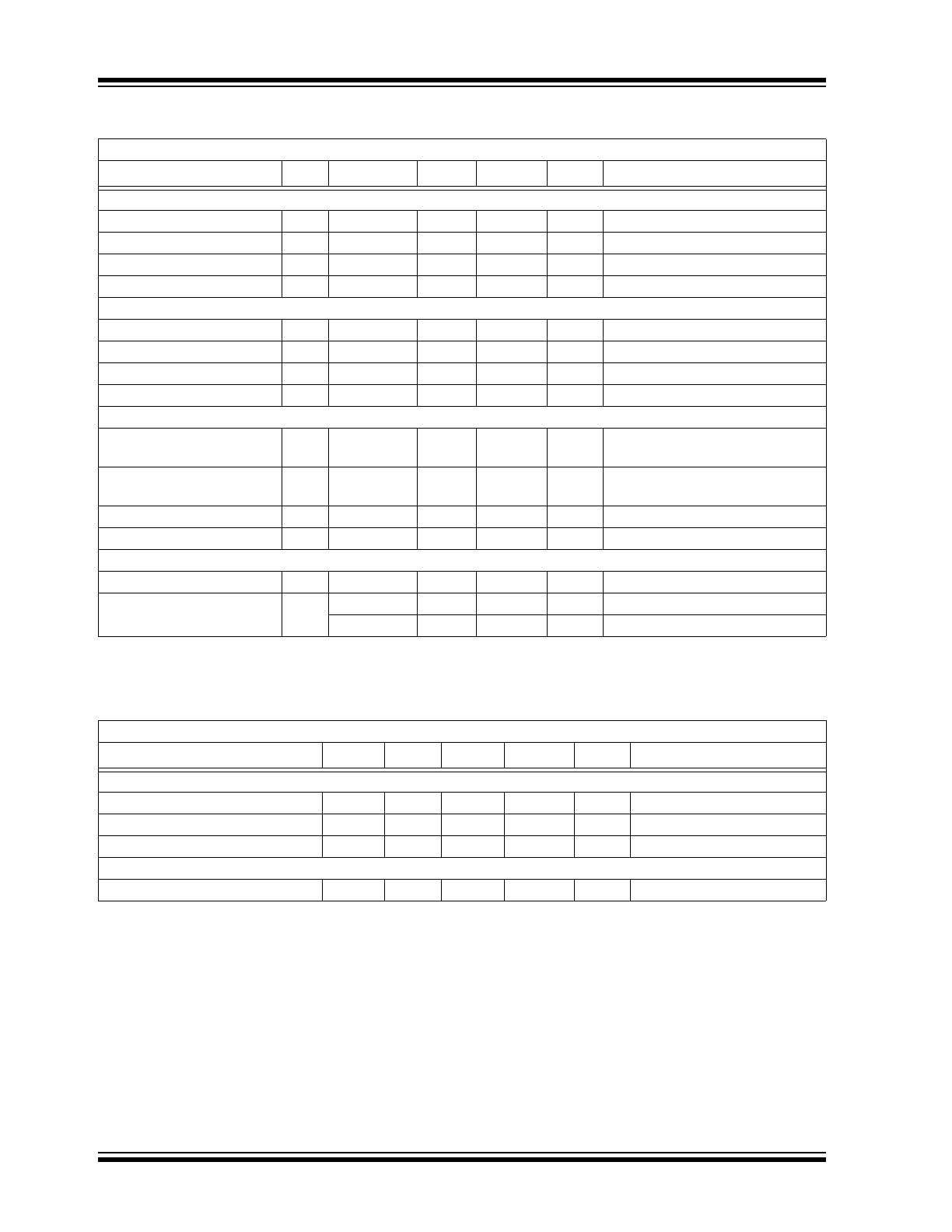
DC CHARACTERISTICS (OVER OPERATING TEMPERATURE RANGE)
Electrical Specifications: Unless otherwise indicated, operating temperature range with 4.5V
V
DD
18V.
Parameters
Sym.
Min.
Typ.
Max.
Units
Conditions
Input
Logic ‘1’, High Input Voltage
V
IH
2.4
—
—
V
Logic ‘0’, Low Input Voltage
V
IL
—
—
0.8
V
Input Current
I
IN
-10
—
+10
µA
0V
V
IN
V
DD
Input Voltage
V
IN
-5
—
V
DD
+ 0.3
V
Output
High Output Voltage
V
OH
V
DD
– 0.025
—
—
V
DC TEST
Low Output Voltage
V
OL
—
—
0.025
V
DC TEST
Output Resistance, High
R
OH
—
16
18
I
OUT
= 10 mA, V
DD
= 18V
Output Resistance, Low
R
OL
—
16
19
I
OUT
= 10 mA, V
DD
= 18V
Switching Time (
Note 1
)
Rise Time
t
R
—
20
30
ns
Figure 4-1
,
Figure 4-2
C
L
= 470 pF
Fall Time
t
F
—
18
28
ns
Figure 4-1
,
Figure 4-2
C
L
= 470 pF
Delay Time
t
D1
—
40
51
ns
Figure 4-1
,
Figure 4-2
Delay Time
t
D2
—
40
51
ns
Figure 4-1
,
Figure 4-2
Power Supply
Supply Voltage
V
DD
4.5
—
18.0
V
Power Supply Current
I
S
—
0.90
1.10
mA
V
IN
= 3V
—
0.11
0.20
mA
V
IN
= 0V
Note 1:
Switching times ensured by design.
2:
Tested during characterization, not production tested.
TEMPERATURE CHARACTERISTICS
Electrical Specifications: Unless otherwise noted, all parameters apply with 4.5V
V
DD
18V.
Parameters
Sym.
Min.
Typ.
Max.
Units
Conditions
Temperature Ranges
Specified Temperature Range
T
A
-40
—
+125
°C
Maximum Junction Temperature
T
J
—
—
+150
°C
Storage Temperature Range
T
A
-65
—
+150
°C
Package Thermal Resistances
Thermal Resistance, 5L-SOT-23
JA
—
220.7
—
°C/W
2007-2014 Microchip Technology Inc.
DS20002052D-page 5
MCP1401/02
2.0
TYPICAL PERFORMANCE CURVES
Note: Unless otherwise indicated, T
A
= +25°C with 4.5V
V
DD
18V.
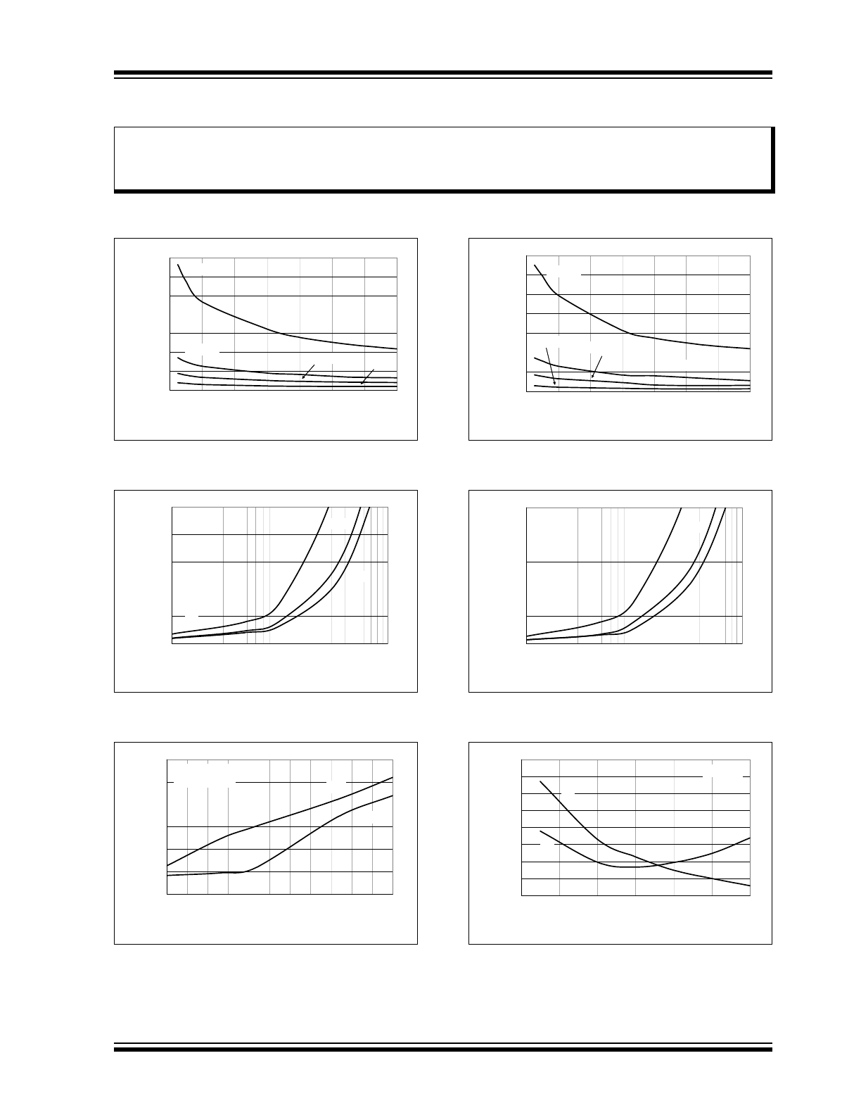
FIGURE 2-1:
Rise Time vs. Supply
Voltage.
FIGURE 2-2:
Rise Time vs. Capacitive
Load.
FIGURE 2-3:
Rise and Fall Times vs.
Temperature.
FIGURE 2-4:
Fall Time vs. Supply
Voltage.
FIGURE 2-5:
Fall Time vs. Capacitive
Load.
FIGURE 2-6:
Propagation Delay vs. Input
Amplitude.
Note:
The graphs and tables provided following this note are a statistical summary based on a limited number of
samples and are provided for informational purposes only. The performance characteristics listed herein
are not tested or guaranteed. In some graphs or tables, the data presented may be outside the specified
operating range (e.g., outside specified power supply range) and therefore outside the warranted range.
0
50
100
150
200
250
300
350
4
6
8
10
12
14
16
18
Supply Voltage (V)
R
ise
T
Ime
(n
s)
3300 pF
470 pF
100 pF
1000 pF
0
50
100
150
200
250
100
1000
10000
Capacitive Load (pF)
Ri
se Ti
m
e
(ns)
5V
18V
12V
10
14
18
22
26
30
34
-40 -25 -10
5
20
35
50
65
80
95 110 125
Temperature (
o
C)
Ti
m
e
(
n
s)
C
LOAD
= 470 pF
V
DD
= 12V
t
FALL
t
RISE
0
50
100
150
200
250
300
350
4
6
8
10
12
14
16
18
Supply Voltage (V)
Fal
l Ti
m
e
(
n
s)
3300 pF
470 pF
100 pF
1000 pF
0
50
100
150
200
250
100
1000
10000
Capacitve Load (pF)
Fal
l Ti
m
e
(
n
s
)
5V
18V
12V
36
37
38
39
40
41
42
43
44
4
5
6
7
8
9
10
Input Amplitude (V)
P
ropagat
ion D
e
lay
(n
s)
t
D2
t
D1
V
DD
= 12V
MCP1401/02
DS20002052D-page 6
2007-2014 Microchip Technology Inc.
Note: Unless otherwise indicated, T
A
= +25°C with 4.5V
V
DD
18V.
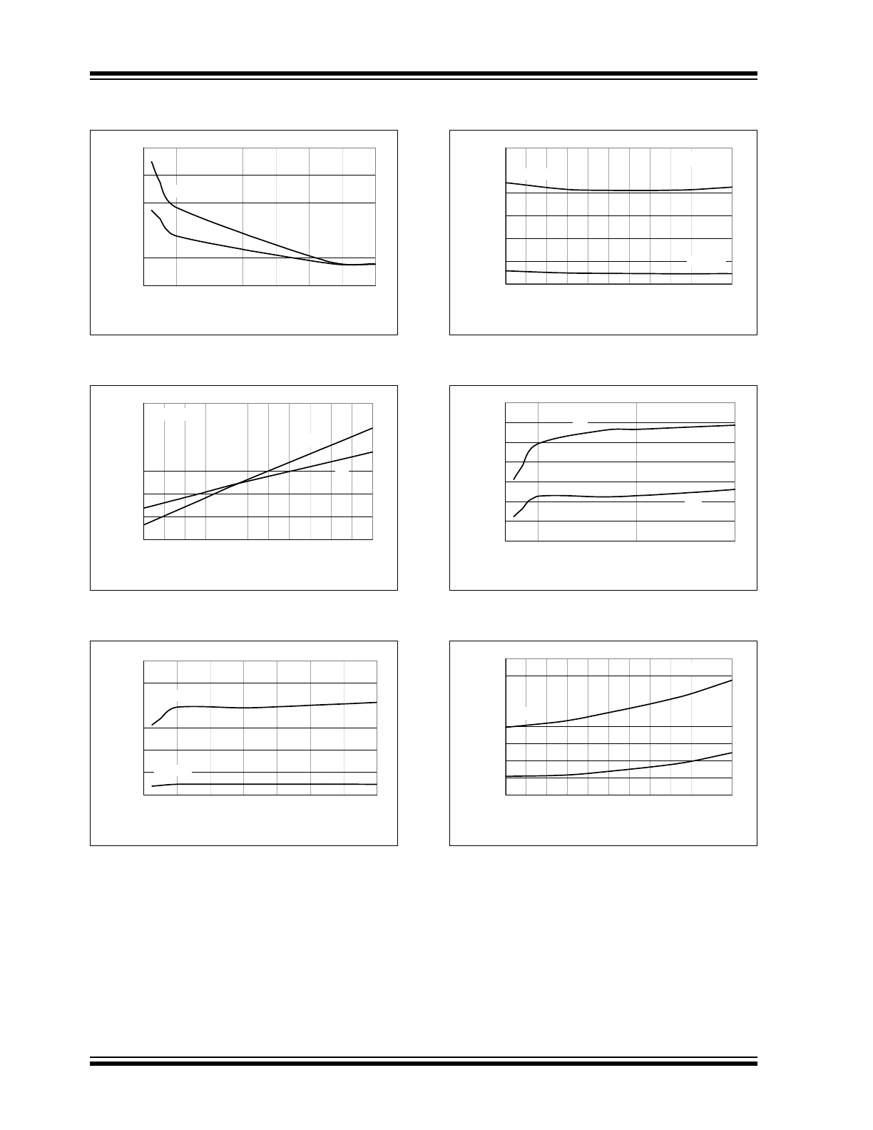
FIGURE 2-7:
Propagation Delay Time vs.
Supply Voltage.
FIGURE 2-8:
Propagation Delay Time vs.
Temperature.
FIGURE 2-9:
Quiescent Current vs.
Supply Voltage.
FIGURE 2-10:
Quiescent Current vs.
Temperature.
FIGURE 2-11:
Input Threshold vs. Supply
Voltage.
FIGURE 2-12:
Input Threshold vs.
Temperature.
Note: Unless otherwise indicated, T
A
= +25°C with 4.5V
V
DD
18V.
30
40
50
60
70
80
4
6
8
10
12
14
16
18
Supply Voltage (V)
P
ropagat
ion D
e
lay
(n
s)
t
D2
t
D1
30
35
40
45
50
55
60
-40 -25 -10
5
20
35
50
65
80
95 110 125
Temperature (
o
C)
P
ropaga
ti
on
D
e
la
y (
n
s)
V
DD
= 12V
t
D2
t
D1
0.0
0.2
0.4
0.6
0.8
1.0
1.2
4
6
8
10
12
14
16
18
Supply Voltage (V)
Quie
scent
C
u
rr
ent (
m
A
)
Input = 1
Input = 0
0.0
0.2
0.4
0.6
0.8
1.0
1.2
-40 -25 -10
5
20 35
50
65
80
95 110 125
Temperature (
o
C)
Qui
e
s
cent Curre
nt
(m
A
)
V
DD
= 18V
Input = 1
Input = 0
1.5
1.6
1.7
1.8
1.9
2
2.1
2.2
4
6
8
10
12
14
16
18
Supply Voltage (V)
Input
Threshol
d
(V
)
V
LO
V
HI
1.6
1.7
1.8
1.9
2
2.1
2.2
2.3
2.4
-40 -25 -10
5
20 35
50
65
80
95 110 125
Temperature (
o
C)
Input
Threshol
d
(V
)
V
DD
= 12V
V
LO
V
HI
2007-2014 Microchip Technology Inc.
DS20002052D-page 7
MCP1401/02
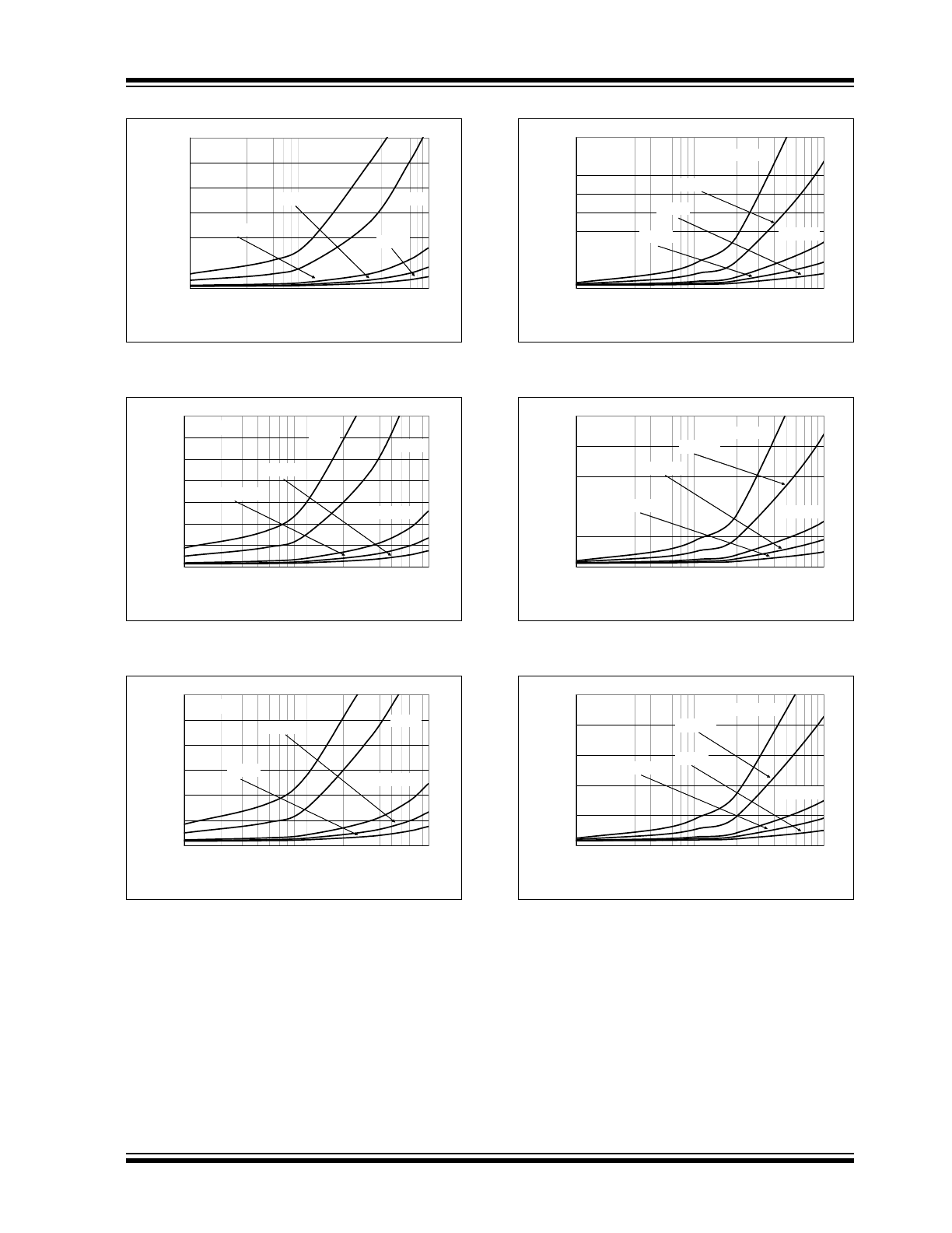
FIGURE 2-13:
Supply Current vs.
Capacitive Load.
FIGURE 2-14:
Supply Current vs.
Capacitive Load.
FIGURE 2-15:
Supply Current vs.
Capacitive Load.
FIGURE 2-16:
Supply Current vs.
Frequency.
FIGURE 2-17:
Supply Current vs.
Frequency.
FIGURE 2-18:
Supply Current vs.
Frequency.
0
25
50
75
100
125
150
100
1000
10000
Capacitive Load (pF)
S
uppl
y
C
u
rrent
(
m
A
)
100 kHz
V
DD
= 18V
2 MHz
1 MHz
200 kHz
50 kHz
0
10
20
30
40
50
60
70
100
1000
10000
Capacitive Load (pF)
S
uppl
y C
u
rre
nt
(
m
A
)
100 kHz
V
DD
= 12V
2 MHz
1 MHz
200 kHz
50 kHz
0
5
10
15
20
25
30
100
1000
10000
Capacitive Load (pF)
S
uppl
y C
u
rre
nt
(
m
A
)
100 kHz
V
DD
= 6V
2 MHz
1 MHz
200 kHz
50 kHz
0
10
20
30
40
50
60
70
80
10
100
1000
Frequency (kHz)
S
uppl
y C
u
rrent
(
m
A
)
V
DD
= 18V
6,800 pF
3,300 pF
1,000 pF
470 pF
100 pF
0
10
20
30
40
50
10
100
1000
Frequency (kHz)
S
uppl
y
V
o
lt
age
(V
)
V
DD
= 12V
6,800 pF
3,300 pF
1,000 pF
470 pF
100 pF
0
5
10
15
20
25
10
100
1000
Frequency (kHz)
S
uppl
y C
u
rre
nt
(
m
A
)
V
DD
= 6V
6,800 pF
3,300 pF
1,000 pF
470 pF
100 pF
MCP1401/02
DS20002052D-page 8
2007-2014 Microchip Technology Inc.
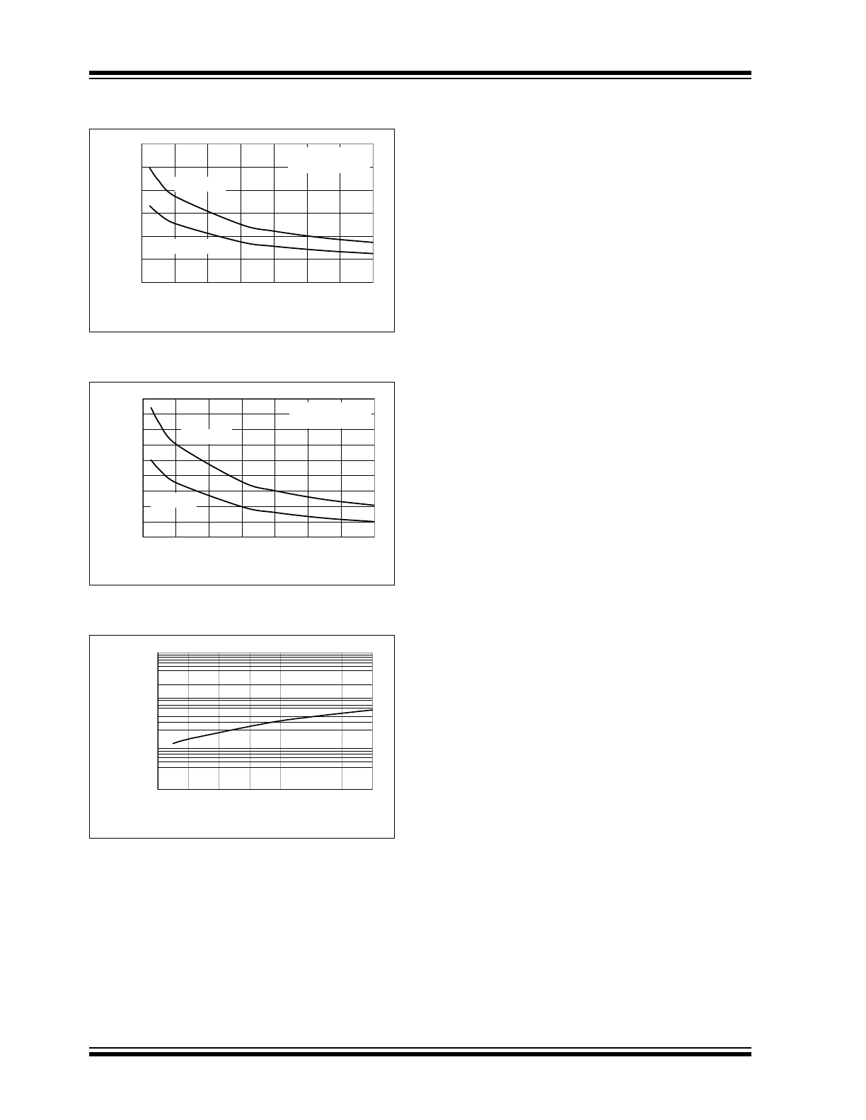
Note: Unless otherwise indicated, T
A
= +25°C with 4.5V
V
DD
18V.
FIGURE 2-19:
Output Resistance (Output
High) vs. Supply Voltage.
FIGURE 2-20:
Output Resistance (Output
Low) vs. Supply Voltage.
FIGURE 2-21:
Crossover Energy vs.
Supply Voltage.
0
10
20
30
40
50
60
4
6
8
10
12
14
16
18
R
OUT
-HI
(ȍ
Supply Voltage (V)
V
IN
= 0V (MCP1401)
V
IN
= 5V (MCP1402)
T
J
= +125
o
C
T
J
= +25
o
C
5
10
15
20
25
30
35
40
45
50
4
6
8
10
12
14
16
18
R
OUT
-LO
(ȍ
Supply Voltage (V)
V
IN
= 5V (MCP1401)
V
IN
= 0V (MCP1402)
T
J
= +125
o
C
T
J
= +25
o
C
1E-10
1E-9
1E-8
1E-7
4
6
8
10
12
14
16
18
Supply Voltage (V)
Cross
o
ver E
n
ergy (A*s
ec)
2007-2014 Microchip Technology Inc.
DS20002052D-page 9
MCP1401/02
3.0
PIN DESCRIPTIONS
The description of the pins are listed in
Table 3-1
.
3.1
Supply Input (V
DD
)
V
DD
is the bias supply input for the MOSFET driver and
has a voltage range of 4.5V to 18V. This input must be
decoupled to ground with a local capacitor. This bypass
capacitor provides a localized low-impedance path for
the peak currents that are to be provided to the load.
3.2
Control Input (IN)
The MOSFET driver input is a high-impedance, TTL/
CMOS-compatible input. The input also has hysteresis
between the high and low input levels, allowing them to
be driven from slow rising and falling signals and to
provide noise immunity.
3.3
Ground (GND)
Ground is the Device Return pin. The Ground pin
should have a low-impedance connection to the bias
supply source return. High peak currents will flow out
the Ground pin when the capacitive load is being
discharged.
3.4
Output (OUT, OUT)
The output is a CMOS push-pull output that is capable
of sourcing and sinking 0.5A of peak current
(V
DD
= 18V). The low output impedance ensures the
gate of the external MOSFET will stay in the intended
state even during large transients. This output also has
a reverse current latch-up rating of 0.5A.
TABLE 3-1:
PIN FUNCTION TABLE
(
1
)
Pin No.
MCP1401
MCP1402
Description
1
GND
GND
Ground
2
V
DD
V
DD
Supply Input
3
IN
IN
Control Input
4
GND
GND
Ground
5
OUT
OUT
Output
Note 1:
Duplicate pins must be connected for proper operation.
MCP1401/02
DS20002052D-page 10
2007-2014 Microchip Technology Inc.
4.0
APPLICATION INFORMATION
4.1
General Information
MOSFET drivers are high-speed, high-current devices
which are intended to source/sink high peak currents to
charge/discharge the gate capacitance of external
MOSFETs or IGBTs. In high-frequency switching power
supplies, the PWM controller may not have the drive
capability to directly drive the power MOSFET. A
MOSFET driver like the MCP1401/02 family can be
used to provide additional source/sink current
capability.
4.2
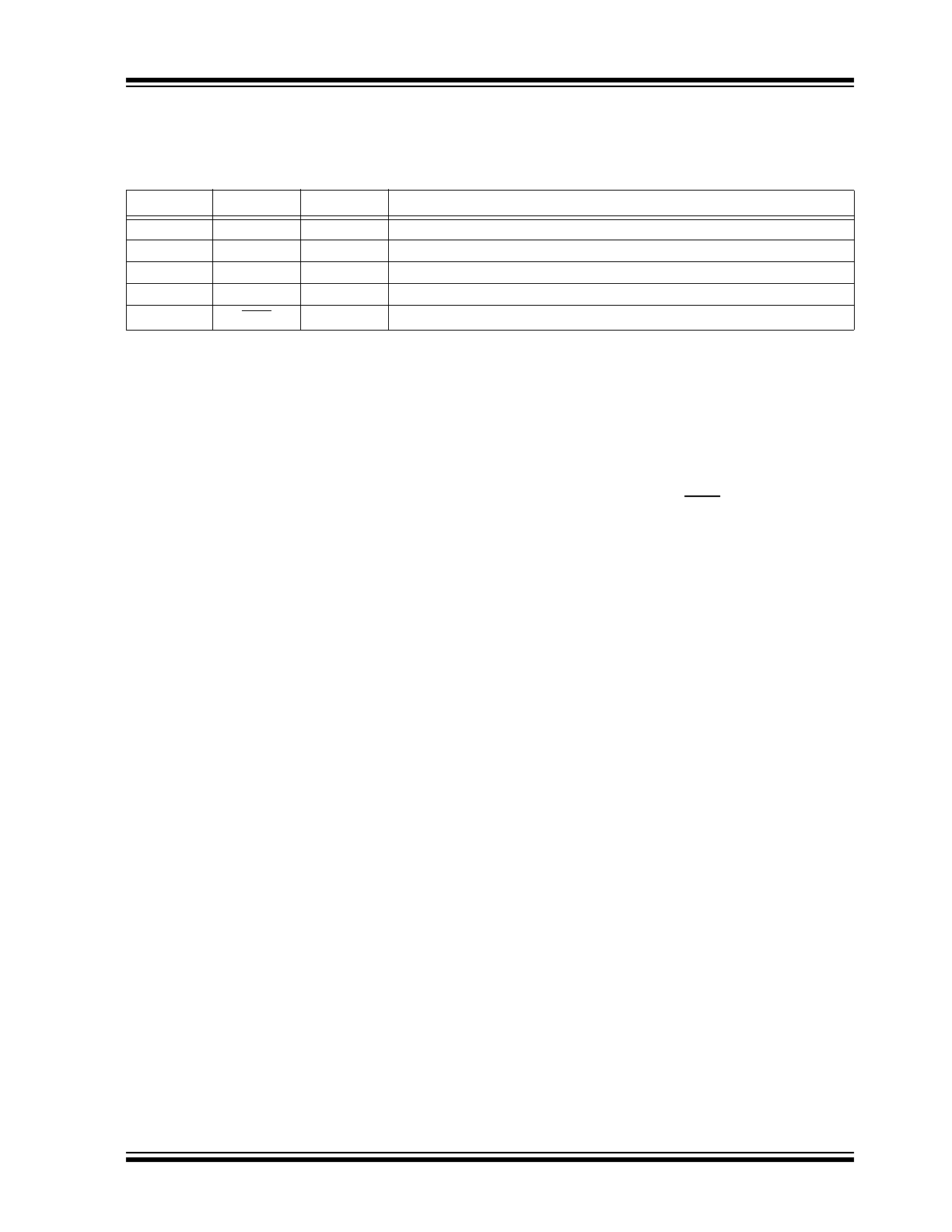
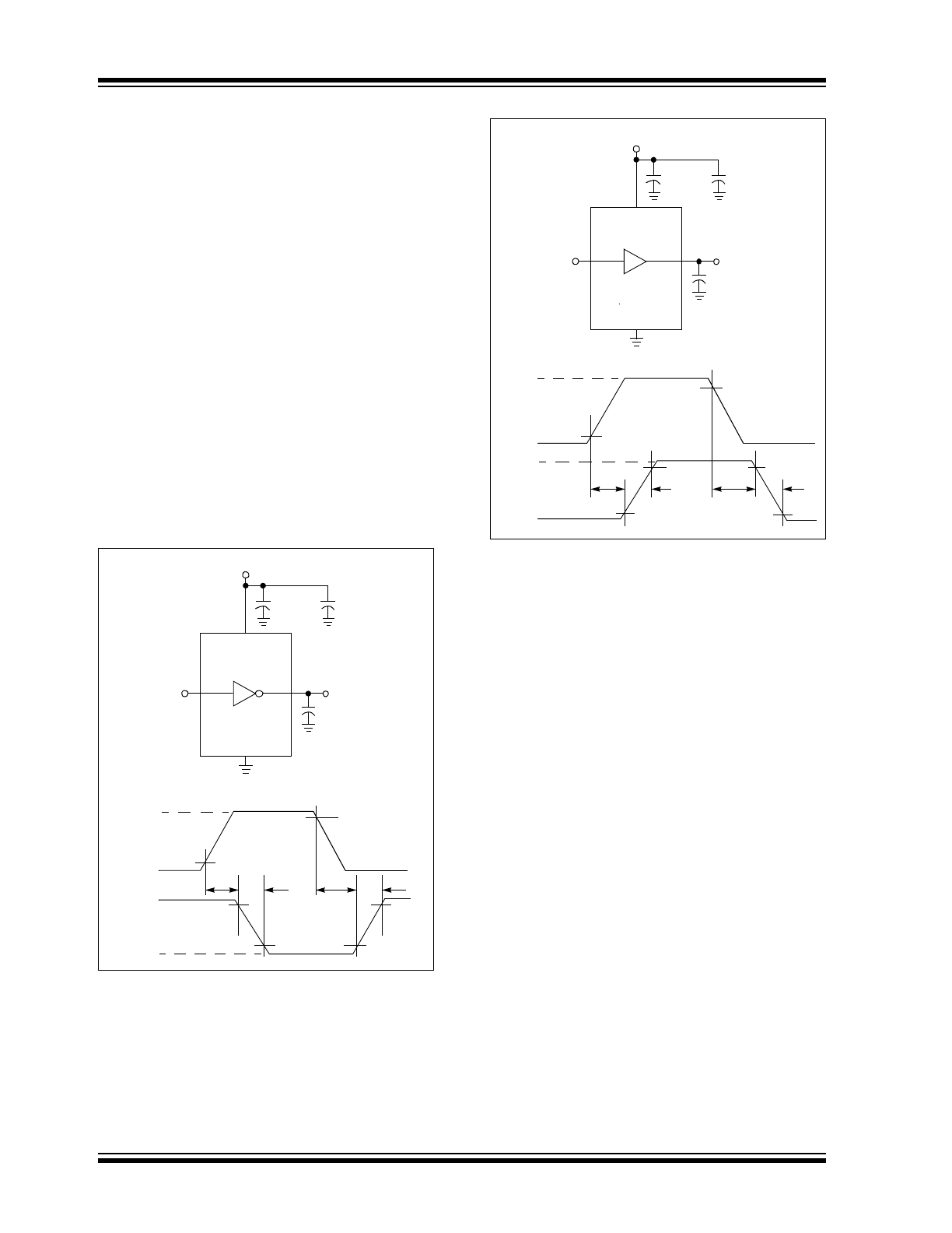
MOSFET Driver Timing
The ability of a MOSFET driver to transition from a fully-
off state to a fully-on state is characterized by the
driver’s rise time (t
R
), fall time (t
F
), and propagation
delays (t
D1
and t
D2
). The MCP1401/02 family of drivers
can typically charge and discharge a 470 pF load
capacitance in 19 ns, along with a typical matched
propagation delay of 35 ns.
Figures 4-1
and
4-2
show
the test circuit and timing waveform used to verify the
MCP1401/02 timing.
FIGURE 4-1:
Inverting Driver Timing
Waveform.
FIGURE 4-2:
Non-Inverting Driver Timing
Waveform.
4.3
Decoupling Capacitors
Careful layout and decoupling capacitors are highly
recommended when using MOSFET drivers. Large
currents are required to charge and discharge
capacitive loads quickly. For example, approximately
550 mA are needed to charge a 470 pF load with 18V
in 15 ns.
To operate the MOSFET driver over a wide frequency
range with low supply impedance, it is recommended to
place a ceramic and low ESR film capacitor in parallel
between the driver V
DD
and GND. A 1.0 µF low ESR
film capacitor and a 0.1 µF ceramic capacitor placed
between pins 2 and 1 should be used. These
capacitors should be placed close to the driver to
minimize circuit board parasitics and provide a local
source for the required current.
4.4
PCB Layout Considerations
Proper Printed Circuit Board (PCB) layout is important
in a high-current, fast switching circuit to provide proper
device operation and robustness of design. PCB trace
loop area and inductance should be minimized by the
use of ground planes or trace under MOSFET gate
drive signals, separate analog and power grounds, and
local driver decoupling.
Placing a ground plane beneath the MCP1401/02 will
help as a radiated noise shield and it will provide some
heat sinking for power dissipated within the device.
0.1 µF
+5V
10%
90%
10%
90%
10%
90%
18V
1 µF
0V
0V
MCP1401
C
L
= 470 pF
Input
Input
Output
t
D1
t
F
t
D2
Output
t
R
V
DD
= 18V
Ceramic
90%
Input
t
D1
t
F
t
D2
Output
t
R
10%
10%
10%
+5V
18V
0V
0V
90%
90%
0.1 µF
1 µF
MCP1402
C
L
= 470 pF
Input
Output
V
DD
= 18V
Ceramic