
TC7662B
TC7662B-8 9/11/96
EVALUATION
KIT
AVAILABLE
© 2001 Microchip Technology Inc. DS21469A
CHARGE PUMP DC-TO-DC VOLTAGE CONVERTER
FEATURES
■
Wide Operating Voltage Range: 1.5V to 15V
■
Boost Pin (Pin 1) for Higher Switching Frequency
■
High Power Efficiency is 96%
■
Easy to Use – Requires Only 2 External Non-Critical
Passive Components
■
Improved Direct Replacement for Industry Stan-
dard ICL7660 and Other Second Source Devices
APPLICATIONS
■
Simple Conversion of +5V to
±
5V Supplies
■
Voltage Multiplication V
OUT
=
±
nV
IN
■
Negative Supplies for Data Acquisition Systems
and Instrumentation
■
RS232 Power Supplies
■
Supply Splitter, V
OUT
=
±
V
S
/2
GENERAL DESCRIPTION
The TC7662B is a pin-compatible upgrade to the Indus-
try standard TC7660 charge pump voltage converter. It
converts a +1.5V to +15V input to a corresponding – 1.5 to
– 15V output using only two low-cost capacitors, eliminating
inductors and their associated cost, size and EMI.
The on-board oscillator operates at a nominal fre-
quency of 10kHz. Frequency is increased to 35kHz when
pin 1 is connected to V
+
, allowing the use of smaller external
capacitors. Operation below 10kHz (for lower supply current
applications) is also possible by connecting an external
capacitor from OSC to ground (with pin 1 open).
The TC7662B is available in both 8-pin DIP and 8-pin
small outline (SO) packages in commercial and extended
temperature ranges.
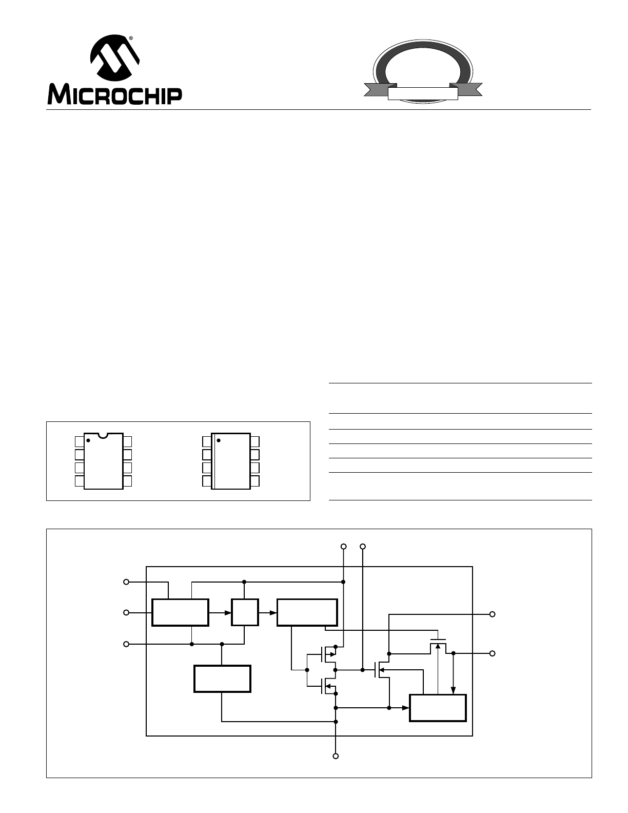
FUNCTIONAL BLOCK DIAGRAM
TC7662B
GND
INTERNAL
VOLTAGE
REGULATOR
RC
OSCILLATOR
VOLTAGE–
LEVEL
TRANSLATOR
÷
2
V + CAP +
8
2
7
6
OSC
LV
3
LOGIC
NETWORK
VOUT
5
CAP –
4
1
BOOST
1
2
3
4
8
7
6
5
TC7662BCPA
TC7662BEPA
BOOST
CAP +
GND
CAP –
VOUT
LOW
VOLTAGE (LV)
OSC
+
V
1
2
3
4
8
7
6
5
TC7662BCOA
TC7662BEOA
BOOST
CAP +
GND
CAP –
VOUT
LOW
VOLTAGE (LV)
OSC
+
V
PIN CONFIGURATION (DIP AND SOIC)
ORDERING INFORMATION
Temperature
Part No.
Package
Range
TC7662BCOA
8-Pin SOIC
0
°
C to +70
°
C
TC7662BCPA
8-Pin Plastic DIP
0
°
C to +70
°
C
TC7662BEOA
8-Pin SOIC
– 40
°
C to +85
°
C
TC7662BEPA
8-Pin Plastic DIP
– 40
°
C to +85
°
C
TC7660EV
Evaluation Kit for
Charge Pump Family
2
TC7662B
CHARGE PUMP DC-TO-DC
VOLTAGE CONVERTER
TC7662B-8 9/11/96
© 2001 Microchip Technology Inc. DS21469A
ELECTRICAL CHARACTERISTICS:
V
+
= 5V, T
A
= +25
°
C, OSC = Free running, Test Circuit Figure 2, Unless
Otherwise Specified.
Symbol
Parameter
Test Conditions
Min
Typ
Max
Unit
I
+
Supply Current (Note 3)
R
L
=
∞
, +25
°
C
—
80
160
µ
A
(Boost pin OPEN OR GND)
0
°
C
≤
T
A
≤
+70
°
C
—
—
180
µ
A
– 40
°
C
≤
T
A
≤
+85
°
C
—
—
180
µ
A
– 55
°
C
≤
T
A
≤
+125
°
C
—
—
200
µ
A
I
+
Supply Current
0
°
C
≤
T
A
≤
+70
°
C
—
—
300
µ
A
(Boost pin = V+)
– 40
°
C
≤
T
A
≤
+85
°
C
350
– 55
°
C
≤
T
A
≤
+125
°
C
400
V
+
H
Supply Voltage Range, High
R
L
= 10 k
Ω
, LV Open, T
MIN
≤
T
A
≤
T
MAX
3.0
—
15
V
(Note 4)
V
+
L
Supply Voltage Range, Low
R
L
= 10 k
Ω
, LV to GND, T
MIN
≤
T
A
≤
T
MAX
1.5
—
3.5
V
R
OUT
Output Source Resistance
I
OUT
= 20mA, 0
°
C
≤
T
A
≤
+70
°
C
—
65
100
Ω
I
OUT
= 20mA, – 40
°
C
≤
T
A
≤
+85
°
C
—
—
120
Ω
I
OUT
= 20mA, – 55
°
C
≤
T
A
≤
+125
°
C
—
—
150
Ω
I
OUT
= 3mA, V
+
= 2V, LV to GND ,
—
—
250
Ω
0
°
C
≤
T
A
≤
+70
°
C
I
OUT
= 3mA, V
+
= 2V, LV to GND ,
—
—
300
Ω
– 40
°
C
≤
T
A
≤
+85
°
C
I
OUT
= 3mA, V
+
= 2V, LV to GND ,
—
—
400
Ω
– 55
°
C
≤
T
A
≤
+125
°
C
f
OSC
Oscillator Frequency
C
OSC
= 0,Pin 1 Open or GND
5
10
—
kHz
Pin 1 = V
+
35
P
Eff
Power Efficiency
R
L
= 5k
Ω
96
96
—
%
T
MIN
≤
T
A
≤
T
MAX
95
97
V
OUT
Eff
Voltage Conversion Efficiency
R
L
=
∞
99
99.9
—
%
Z
OSC
Oscillator Impedance
V
+
= 2V
—
1
—
M
Ω
V
+
= 5V
—
100
—
k
Ω
NOTES:
1. Connecting any terminal to voltages greater than V+ or less than GND may cause destructive latch-up. It is recommended that no inputs from
sources operating from external supplies be applied prior to “power up” of the TC7662B.
2. Derate linearly above 50
°
C by 5.5 mW/
°
C.
3. In the test circuit, there is no external capacitor applied to pin 7. However, when the device is plugged into a test socket, there is usually a very
small but finite stray capacitance present, of the order of 5pF.
4. The TC7662B can operate without an external diode over the full temperature and voltage range. This device will function in existing designs which
incorporate an external diode with no degradation in overall circuit performance.
ABSOLUTE MAXIMUM RATINGS*
Supply Voltage ...................................................... +16.5V
LV, Boost and OSC Inputs Voltage (Note 1)
V+<5.5V ..................................... – 0.3V to (V
+
+ 0.3V)
>5.5V .................................. (V
+
– 5.5V) to (V
+
+ 0.3V)
Current Into LV (Note 1)
V
+
>3.5V ............................................................ 20
µ
A
Output Short Duration
(V
SUPPLY
≤
5.5V) ....................................... Continuous
Power Dissipation (T
A
≤
70
°
C) (Note 2)
Plastic DIP ...................................................... 730mW
SO .................................................................. 470mW
Operating Temperature Range
C Suffix .................................................. 0
°
C to +70
°
C
E Suffix ............................................. – 40
°
C to +85
°
C
Storage Temperature Range ................ – 65
°
C to +150
°
C
Lead Temperature (Soldering, 10 sec) ................. +300
°
C
* Static-sensitive device. Unused devices must be stored in conductive
material. Protect devices from static discharge and static fields. Stresses
above those listed under "Absolute Maximum Ratings" may cause perma-
nent damage to the device. These are stress ratings only and functional
operation of the device at these or any other conditions above those
indicated in the operation sections of the specifications is not implied.
Exposure to absolute maximum rating conditions for extended periods
may affect device reliability.
3
TC7662B
CHARGE PUMP DC-TO-DC
VOLTAGE CONVERTER
TC7662B-8 9/11/96
© 2001 Microchip Technology Inc. DS21469A
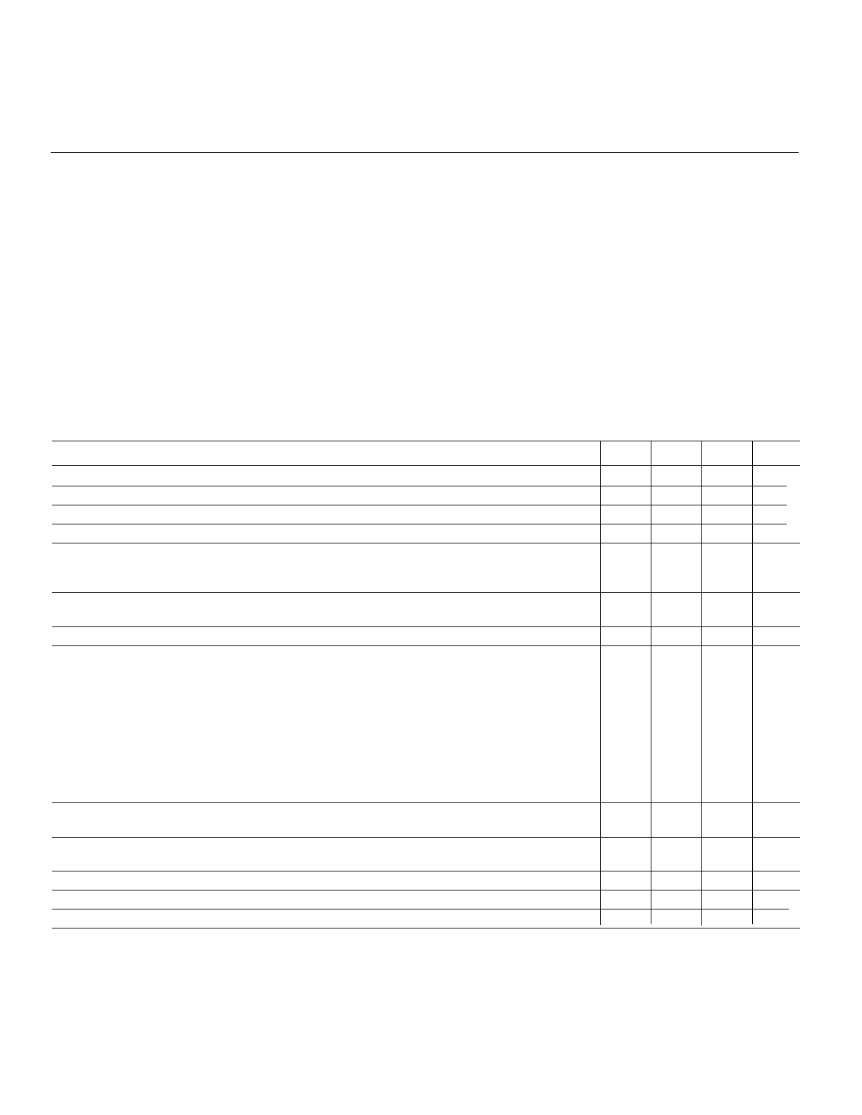
Figure 2. Idealized Negative Voltage Capacitor
THEORETICAL POWER EFFICIENCY
CONSIDERATIONS
In theory, a voltage converter can approach 100%
efficiency if certain conditions are met:
A. The drive circuitry consumes minimal power.
B. The output switches have extremely low ON resistance
and virtually no offset.
C. The impedances of the pump and reservoir capacitors
are negligible at the pump frequency.
The TC7662B approaches these conditions for nega-
tive voltage conversion if large values of C
1
and C
2
are used.
Energy is lost only in the transfer of charge between
capacitors if a change in voltage occurs. The energy lost
is defined by:
E = 1/2 C
1
(V
1
2
– V
2
2
)
where V
1
and V
2
are the voltages on C
1
during the pump and
transfer cycles. If the impedances of C
1
and C
2
are relatively
high at the pump frequency (refer to Figure 2) compared to
the value of R
L
, there will be a substantial difference in
voltages V
1
and V
2
. Therefore, it is desirable not only to
make C
2
as large as possible to eliminate output voltage
ripple, but also to employ a correspondingly large value for
C
1
in order to achieve maximum efficiency of operation.
Dos and Don’ts
1. Do not exceed maximum supply voltages.
2. Do not connect the LV terminal to GND for supply
voltages greater than 3.5 volts.
3. Do not short circuit the output to V
+
supply for voltages
above 5.5 volts for extended periods; however,
transient conditions including start-up are okay.
DETAILED DESCRIPTION
The TC7662B contains all the necessary circuitry to
complete a negative voltage converter, with the exception of
two external capacitors which may be inexpensive 1
µ
F
polarized electrolytic types. The mode of operation of the
device may be best understood by considering Figure 2,
which shows an idealized negative voltage converter. Ca-
pacitor C
1
is charged to a voltage V
+
for the half cycle when
switches S
1
and S
3
are closed. (Note: Switches S
2
and S
4
are open during this half cycle.) During the second half cycle
of operation, switches S
2
and S
4
are closed, with S
1
and S
3
open, thereby shifting capacitor C
1
negatively by V
+
volts.
Charge is then transferred from C
1
to C
2
such that the
voltage on C
2
is exactly V
+
, assuming ideal switches and no
load on C
2
. The TC7662B approaches this ideal situation
more closely than existing non-mechanical circuits.
In the TC7662B, the four switches of Figure 2 are MOS
power switches; S
1
is a P-channel device and S
2
, S
3
and S
4
are N-channel devices. The main difficulty with this ap-
proach is that in integrating the switches, the substrates of
S
3
and S
4
must always remain reverse biased with respect
to their sources, but not so much as to degrade their “ON”
resistances. In addition, at circuit start up, and under output
short circuit conditions (V
OUT
= V
+
), the output voltage must
be sensed and the substrate bias adjusted accordingly.
Failure to accomplish this would result in high power losses
and probable device latchup.
The problem is eliminated in the TC7662B by a logic
network which senses the output voltage (V
OUT
) together
with the level translators, and switches the substrates of S
3
and S
4
to the correct level to maintain necessary reverse
bias.
The voltage regulator portion of the TC7662B is an
integral part of the anti-latchup circuitry; however, its inher-
ent voltage drop can degrade operation at low voltages.
Therefore, to improve low voltage operation, the “LV” pin
should be connected to GND, disabling the regulator. For
supply voltages greater than 3.5 volts, the LV terminal must
be left open to insure latchup proof operation and prevent
device damage.
Figure 1. TC7662B Test Circuit
1
2
3
4
8
7
6
5
TC7662B
+
V+
(+5V)
V+
VO
C1
10
µ
F
+
C2
10
µ
F
IL
RL
NOTE:
For large values of C
OSC
(>1000 pF), the values
of C
1
and C
2
should be increased to 100 µF.
IS
VIN
S3
S1
S2
S4
C2
VOUT = – VIN
C1
4
TC7662B
CHARGE PUMP DC-TO-DC
VOLTAGE CONVERTER
TC7662B-8 9/11/96
© 2001 Microchip Technology Inc. DS21469A
4. When using polarized capacitors in the inverting mode,
the + terminal of C
1
must be connected to pin 2 of the
TC7662B and the – terminal of C
2
must be connected
to GND.
5. If the voltage supply driving the TC7662B has a large
source impedance (25-30 ohms), then a 2.2
µ
F capaci-
tor from pin 8 to ground may be required to limit the
rate of rise of the input voltage to less than 2V/
µ
sec.
TYPICAL APPLICATIONS
Simple Negative Voltage Converter
The majority of applications will undoubtedly utilize the
TC7662B for generation of negative supply voltages. Figure
3 shows typical connections to provide a negative supply
where a positive supply of +1.5V to +15V is available. Keep
in mind that pin 6 (LV) is tied to the supply negative (GND)
for supply voltages below 3.5 volts.
a.
b.
The output characteristics of the circuit in Figure 3 can
be approximated by an ideal voltage source in series with a
resistance as shown in Figure 3b. The voltage source has a
value of–(V+). The output impedance (R
O
) is a function of
the ON resistance of the internal MOS switches (shown in
Figure 2), the switching frequency, the value of C
1
and C
2
,
and the ESR (equivalent series resistance) of C
1
and C
2
. A
good first order approximation for R
O
is:
R
O
≅
2(R
SW1
+ R
SW3
+ ESR
C1
) + 2(R
SW2
+ R
SW4
+
ESR
C1
) + + ESR
C2
(f
PUMP
= , R
SWX
= MOSFET switch resistance)
Combining the four R
SWX
terms as R
SW
, we see that:
R
O
≅
2 x R
SW
+ + 4 x ESR
C1
+ ESR
C2
Ω
R
SW
, the total switch resistance, is a function of supply
1
f
PUMP
x C
1
f
OSC
2
1
f
PUMP
x C
1
t
2
t
1
B
A
V
–
(V+)
0
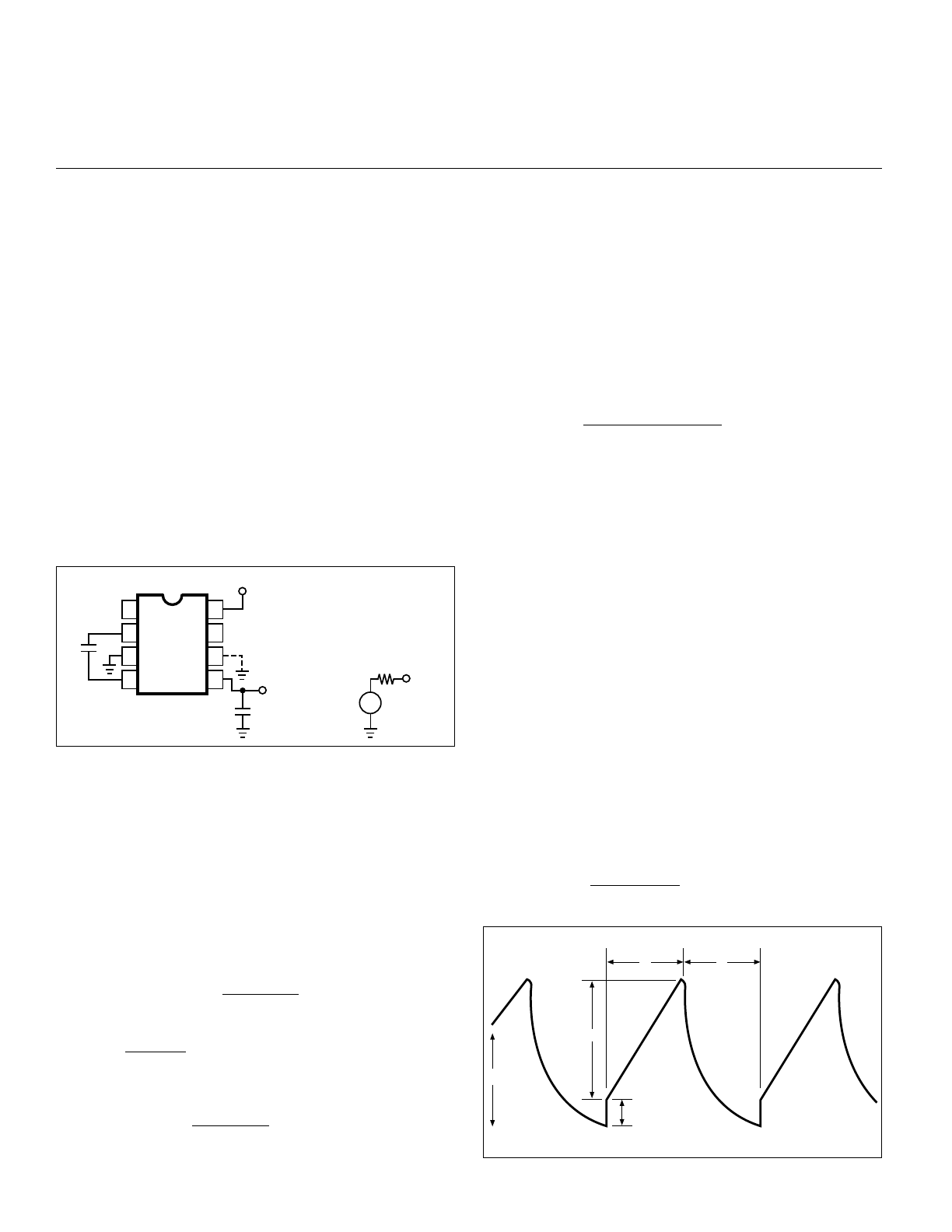
Figure 4. Output Ripple
Figure 3. Simple Negative Converter and its Output Equivalent
1
2
3
4
8
7
6
5
TC7662B
10
µ
F
+
V+
+
10
µ
F
VOUT = –V+
–
–
VOUT
RO
V+
+
–
1
2 x f
PUMP
x C
2
1
(5 x 10
3
x 10 x 10
-6
)
voltage and temperature (See the Output Source Resis-
tance graphs), typically 23
Ω
at +25
°
C and 5V. Careful
selection of C
1
and C
2
will reduce the remaining terms,
minimizing the output impedance. High value capacitors will
reduce the 1/(f
PUMP
x C
1
) component, and low ESR capaci-
tors will lower the ESR term. Increasing the oscillator fre-
quency will reduce the 1/(f
PUMP
x C
1
) term, but may have the
side effect of a net increase in output impedance when C
1
>
10
µ
F and there is not enough time to fully charge the
capacitors every cycle. In a typical application when f
OSC
=
10kHz and C = C
1
= C
2
= 10
µ
F:
R
O
≅
2 x 23 + + 4 x ESR
C1
+ ESR
C2
R
O
≅
(46 + 20 + 5 x ESR
C
)
Ω
Since the ESRs of the capacitors are reflected in the
output impedance multiplied by a factor of 5, a high value
could potentially swamp out a low 1/(f
PUMP
x C
1
) term,
rendering an increase in switching frequency or filter capaci-
tance ineffective. Typical electrolytic capacitors may have
ESRs as high as 10
Ω
.
Output Ripple
ESR also affects the ripple voltage seen at the output.
The total ripple is determined by 2 voltages, A and B, as
shown in Figure 4. Segment A is the voltage drop across the
ESR of C
2
at the instant it goes from being charged by C
1
(current flowing into C
2
) to being discharged through the
load (current flowing out of C
2
). The magnitude of this
current change is 2 x I
OUT
, hence the total drop is 2 x I
OUT
x
ESR
C2
volts. Segment B is the voltage change across C
2
during time t
2
, the half of the cycle when C
2
supplies current
to the load. The drop at B is I
OUT
x t
2
/C
2
volts. The peak-to-
peak ripple voltage is the sum of these voltage drops:
V
RIPPLE
≅
(
+ ESR
C2
x I
OUT
)
5
TC7662B
CHARGE PUMP DC-TO-DC
VOLTAGE CONVERTER
TC7662B-8 9/11/96
© 2001 Microchip Technology Inc. DS21469A
Paralleling Devices
Any number of TC7662B voltage converters may be
paralleled to reduce output resistance (Figure 5). The reser-
voir capacitor, C
2
, serves all devices, while each device
requires its own pump capacitor, C
1
. The resultant output
resistance would be approximately:
R
OUT
(of TC7662B)
n (number of devices)
R
OUT
=
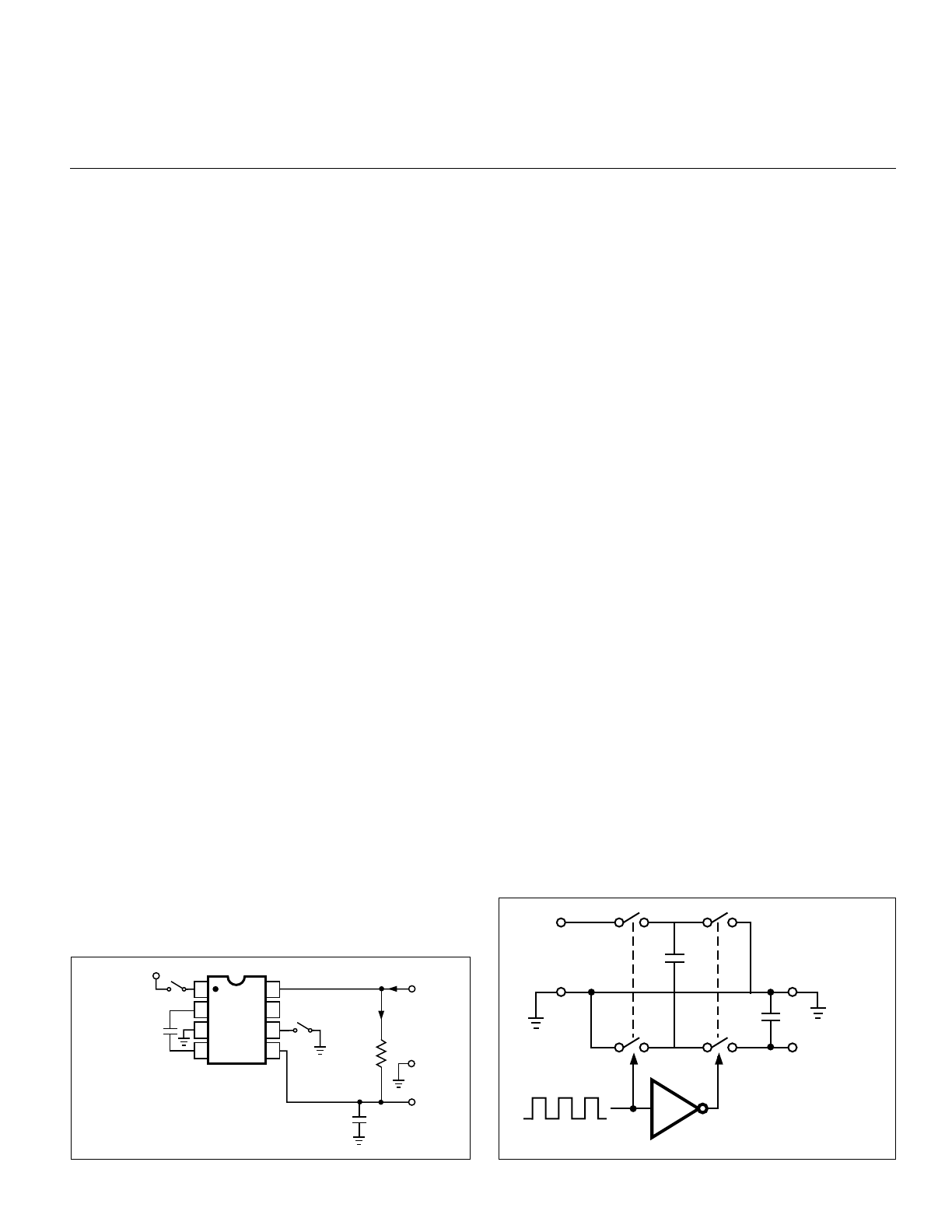
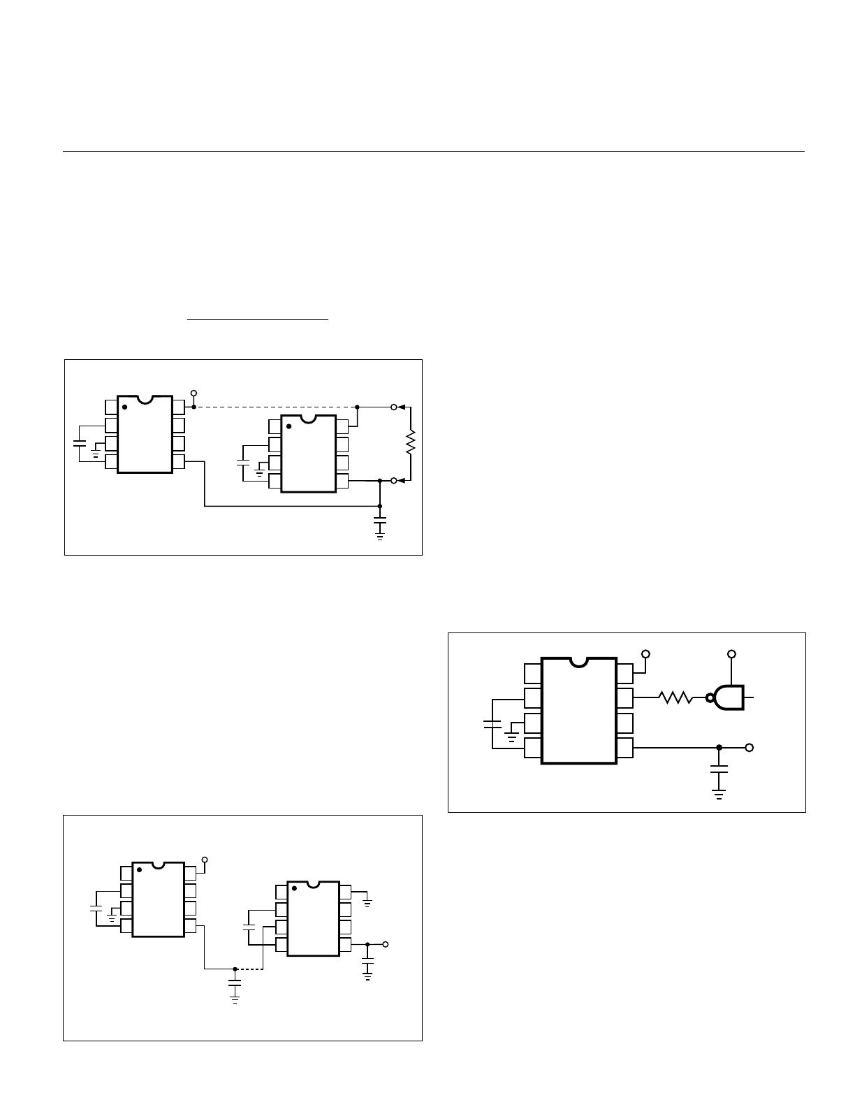
Changing the TC7662B Oscillator Frequency
It may be desirable in some applications (due to noise or
other considerations) to increase the oscillator frequency.
This is achieved by one of several methods described
below:
By connecting the BOOSTPin (Pin 1) to V
+
, the oscillator
charge and discharge current is increased and, hence the
oscillator frequency is increased by approximately 3-1/2
times. The result is a decrease in the output impedance and
ripple. This is of major importance for surface mount appli-
cations where capacitor size and cost are critical. Smaller
capacitors, e.g., 0.1
µ
F, can be used in conjunction with the
Boost Pin in order to achieve similar output currents com-
pared to the device free running with C
1
= C
2
= 1
µ
F or 10
µ
F.
(Refer to graph of Output Source Resistance as a Function
of Oscillator Frequency).
Increasing the oscillator frequency can also be achieved
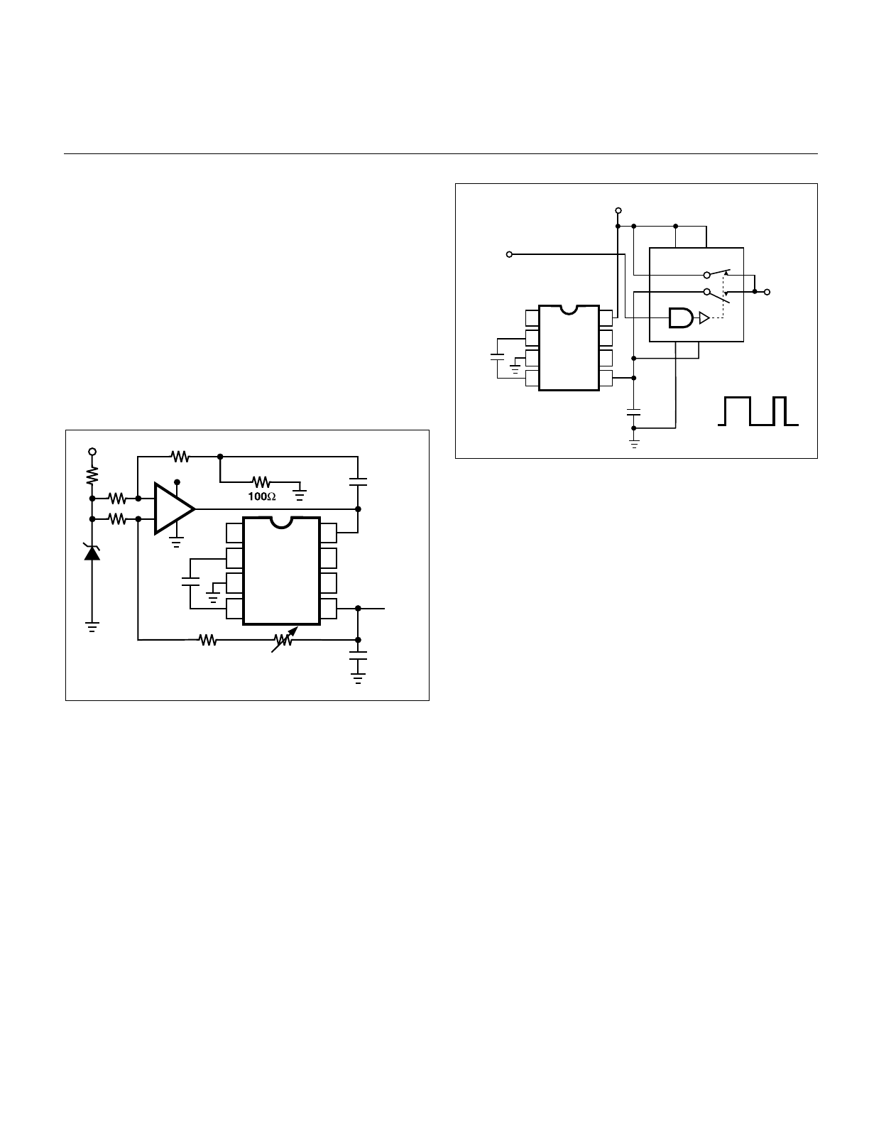
by overdriving the oscillator from an external clock as shown
in Figure 7. In order to prevent device latchup, a 1k
Ω
resistor
must be used in series with the clock output. In a situation
where the designer has generated the external clock fre-
quency using TTL logic, the addition of a 10k
Ω
pullup
resistor to V
+
supply is required. Note that the pump fre-
quency with external clocking, as with internal clocking, will
be 1/2 of the clock frequency. Output transitions occur on the
positive-going edge of the clock.
Figure 6. Cascading Devices for Increased Output Voltage
1
2
3
4
8
7
6
5
V+
1
2
3
4
8
7
6
5
10
µ
F
10
µ
F
"n"
"1"
10
µ
F
VOUT
*VOUT = –nV+
+
+
+
TC7662B
TC7662B
10
µ
F
Cascading Devices
The TC7662B may be cascaded as shown to produce
larger negative multiplication of the initial supply voltage.
However, due to the finite efficiency of each device, the
practical limit is 10 devices for light loads. The output voltage
is defined by:
V
OUT
= – n(V
IN
)
where n is an integer representing the number of devices
cascaded. The resulting output resistance would be ap-
proximately the weighted sum of the individual TC7662B
R
OUT
values.
Figure 5. Paralleling Devices
1
2
3
4
8
7
6
5
TC7662B
+
V +
+
CMOS
GATE
10
µ
F
VOUT
10
µ
F
1 k
Ω
V +
Figure 7. External Clocking
It is also possible to increase the conversion efficiency
of the TC7662B at low load levels by lowering the oscillator
frequency. This reduces the switching losses, and is shown
in Figure 8. However, lowering the oscillator frequency will
cause an undesirable increase in the impedance of the
pump (C
1
) and reservoir (C
2
) capacitors; this is overcome by
increasing the values of C
1
and C
2
by the same factor that
the frequency has been reduced. For example, the addition
of a 100pF capacitor between pin 7 (Osc) and V
+
will lower
the oscillator frequency to 1kHz from its nominal frequency
of 10kHz (multiple of 10), and thereby necessitate a corre-
sponding increase in the value of C
1
and C
2
(from 10
µ
F to
100
µ
F).
1
2
3
4
8
7
6
5
TC7662B
V
+
1
2
3
4
8
7
6
5
TC7662B
C1
RL
C2
C1
"n"
"1"
+
6
TC7662B
CHARGE PUMP DC-TO-DC
VOLTAGE CONVERTER
TC7662B-8 9/11/96
© 2001 Microchip Technology Inc. DS21469A
1
2
3
4
8
7
6
5
+
V
+
VOUT
C1
COSC
+
C2
TC7662B
Figure 8. Lowering Oscillator Frequency
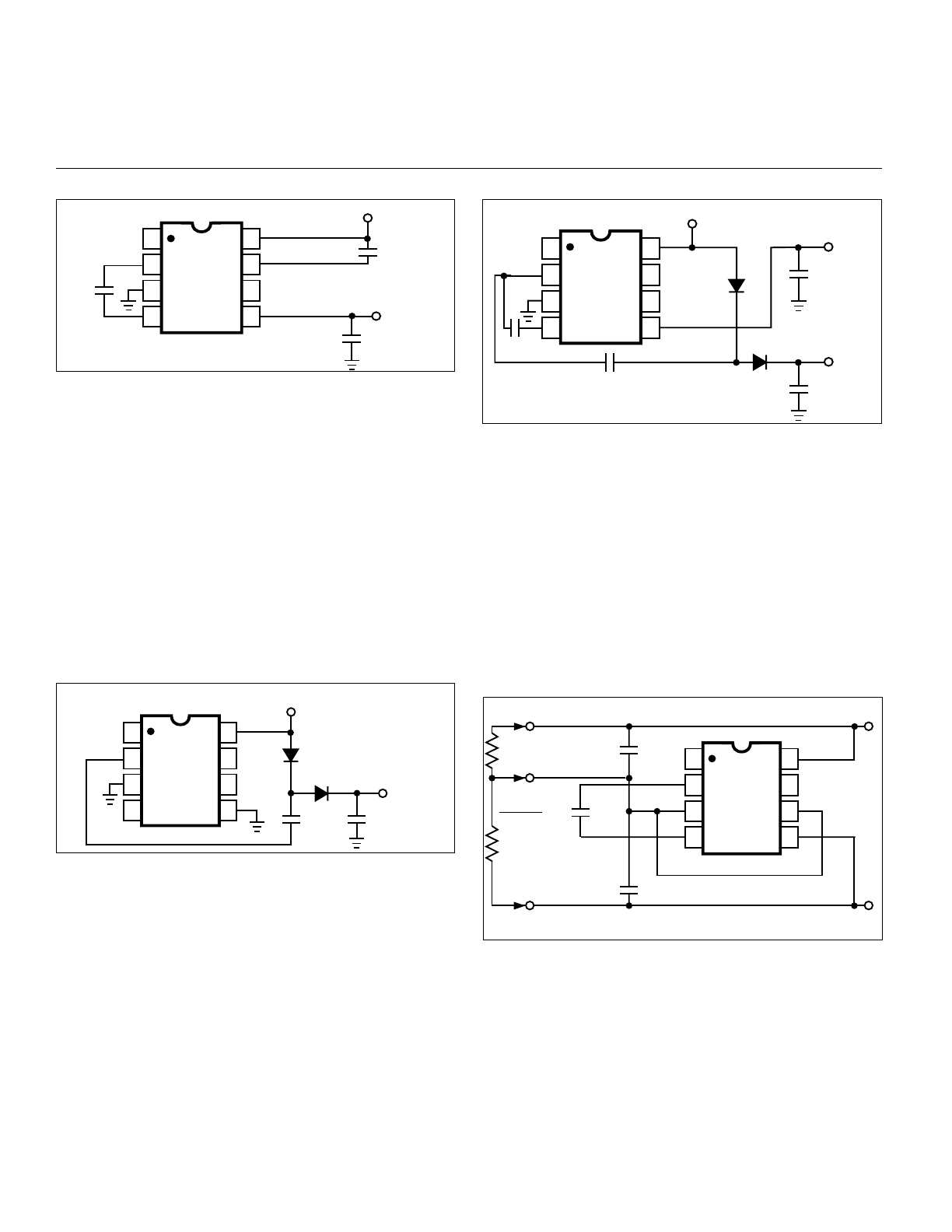
Positive Voltage Doubling
The TC7662B may be employed to achieve positive
voltage doubling using the circuit shown in Figure 9. In this
application, the pump inverter switches of the TC7662B are
used to charge C
1
to a voltage level of V
+
– V
F
(where V
+
is
the supply voltage and V
F
is the forward voltage on C
1
plus
the supply voltage (V
+
) applied through diode D
2
to capacitor
C
2
). The voltage thus created on C
2
becomes (2 V
+
) – (2 V
F
),
or twice the supply voltage minus the combined forward
voltage drops of diodes D
1
and D
2
.
The source impedance of the output (V
OUT
) will depend
on the output current, but for V
+
= 5V and an output current
of 10 mA, it will be approximately 60
Ω
.
Combined Negative Voltage Conversion
and Positive Supply Multiplication
Figure 10 combines the functions shown in Figures 3
and 9 to provide negative voltage conversion and positive
voltage doubling simultaneously. This approach would be,
for example, suitable for generating +9V and –5V from an
existing +5V supply. In this instance, capacitors C
1
and C
3
perform the pump and reservoir functions, respectively, for
the generation of the negative voltage, while capacitors C
2
and C
4
are pump and reservoir, respectively, for the doubled
positive voltage. There is a penalty in this configuration
which combines both functions, however, in that the source
impedances of the generated supplies will be somewhat
higher due to the finite impedance of the common charge
pump driver at pin 2 of the device.
1
2
3
4
8
7
6
5
+
V +
VOUT =
(2 V +) – (2 VF)
C1
D1
+
+
C3
C4
VOUT =
– (V+– VF)
C2
TC7662B
D2
+
Figure 10. Combined Negative Converter and Positive Doubler
Figure 9. Positive Voltage Multiplier
Voltage Splitting
The bidirectional characteristics can also be used to
split a higher supply in half, as shown in Figure 11. The
combined load will be evenly shared between the two sides
and a high value resistor to the LV pin ensures start-up.
Because the switches share the load in parallel, the output
impedance is much lower than in the standard circuits, and
higher currents can be drawn from the device. By using this
circuit, and then the circuit of Figure 6, +15V can be
converted (via +7.5V and –7.5V) to a nominal –15V, though
with rather high series resistance (~250
Ω
).
1
2
3
4
8
7
6
5
V+
VOUT =
(2 V+) – (2 VF)
+
C2
D1
D2
+
C1
TC7662B
+
RL1
RL2
VOUT =
V + –V –
2
50
µ
F
50
µ
F
V +
V –
50
µ
F
+
1
2
8
7
TC7662B
3
4
6
5
-
-
+
-
Figure 11. Splitting a Supply in Half
7
TC7662B
CHARGE PUMP DC-TO-DC
VOLTAGE CONVERTER
TC7662B-8 9/11/96
© 2001 Microchip Technology Inc. DS21469A
1
2
3
4
8
7
6
5
TC7662B
1
µ
F
+
+
1
µ
F
–
+5 LOGIC SUPPLY
TTL DATA
INPUT
RS232
DATA
OUTPUT
11
3
12
16
4
15
13
14
1
IH5142
+5V
-5V
Figure 13. RS232 Levels from a Single 5V Supply
Regulated Negative Voltage Supply
In some cases, the output impedance of the TC7662B
can be a problem, particularly if the load current varies
substantially. The circuit of Figure 12 can be used to over-
come this by controlling the input voltage, via an ICL7611
low-power CMOS op amp, in such a way as to maintain a
nearly constant output voltage. Direct feedback is advisable,
since the TC7662B’s output does not respond instanta-
neously to change in input, but only after the switching delay.
The circuit shown supplies enough delay to accommodate
the TC7662B, while maintaining adequate feedback. An
increase in pump and storage capacitors is desirable, and
the values shown provide an output impedance of less than
5
Ω
to a load of 10mA.
1
2
3
4
8
7
6
5
TC7662B
100
µ
F
+
V+
100
µ
F
V
OUT
-
50k
100k
+8V
50k
10
µ
F
–
+
800k
250K
VOLTAGE
ADJUST
+8V
56k
–
+
Figure 12. Regulating the Output Voltage
8
TC7662B
CHARGE PUMP DC-TO-DC
VOLTAGE CONVERTER
TC7662B-8 9/11/96
© 2001 Microchip Technology Inc. DS21469A
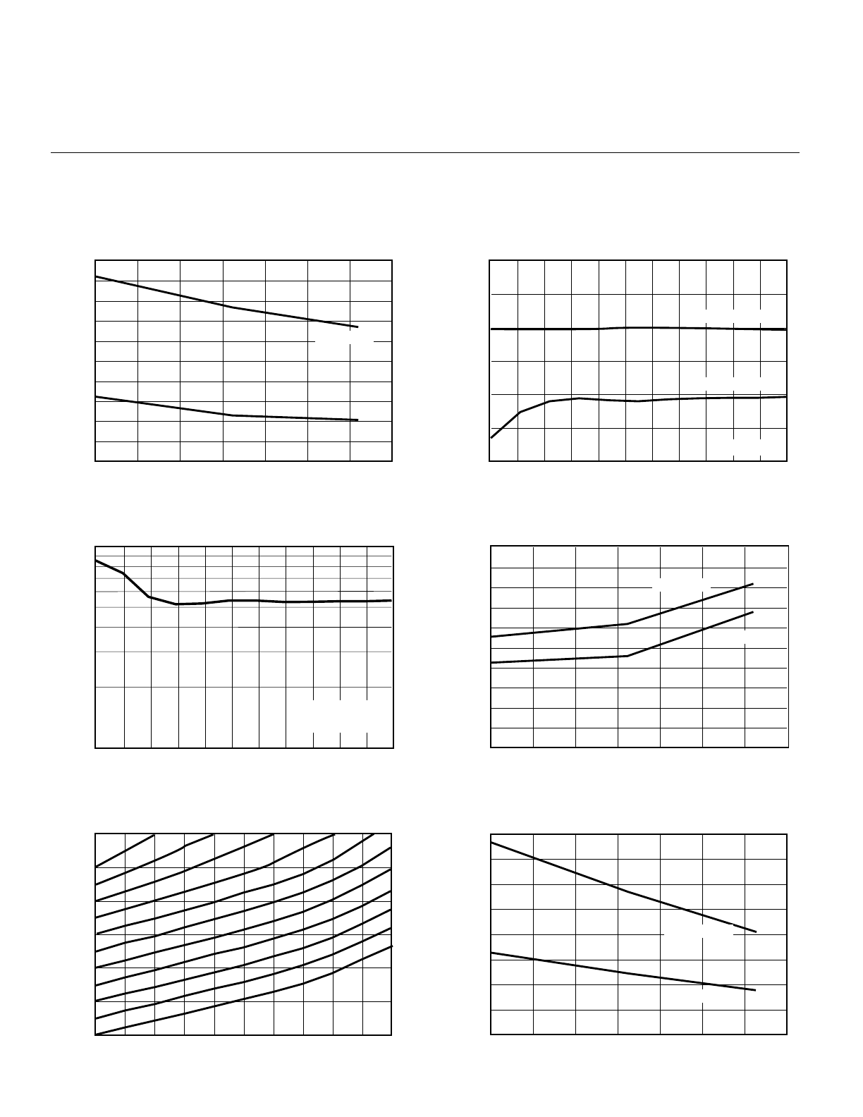
TYPICAL CHARACTERISTICS
Supply Current vs. Temperature
(with Boost Pin = V
IN
)
1000
0
200
400
600
800
-40
-20
0
20
40
100
60
80
I
DD
(
µ
A)
TEMPERATURE (
°
C)
V
IN
= 12V
Without Load
10K Load
Voltage Conversion
101.0
100.5
100.0
99.5
99.0
98.5
98.0
1
12
11
10
9
8
7
5
6
4
2
3
VOLTAGE CONVERSION EFFICIENCY (%)
INPUT VOLTAGE V
IN
(V)
Output Voltage vs. Output Current
0
-2
-4
-6
-8
-10
-12
OUTPUT VOLTAGE V
OUT
(V)
OUTPUT CURRENT (mA)
V
IN
= 5V
I
OUT
= 20mA
T
A
= 25
°
C
Supply Current vs. Temperature
200
150
125
175
100
75
50
25
0
SUPPLY CURRENT I
DD
(
µ
A)
TEMPERATURE (
°
C)
0
100
90
80
70
60
40
50
30
10
20
1.5
12
11.5
10.5
9.5
8.5
7.5
5.5 6.5
4.5
2.5 3.5
Output Source Resistance vs. Supply Voltage
100
10
30
50
70
OUTPUT SOURCE RESISTANCE (
Ω
)
SUPPLY VOLTAGE (V)
Output Source Resistance vs. Temperature
100
0
20
40
60
80
-40
-20
0
20
40
100
60
80
OUTPUT SOURCE RESISTANCE (
Ω
)
TEMPERATURE (
°
C)
V
IN
= 2.5V
V
IN
= 5.5V
-40
-20
0
20
40
100
60
80
V
IN
= 12.5V
V
IN
= 5.5V
T
A
= 25
°
C
9
TC7662B
CHARGE PUMP DC-TO-DC
VOLTAGE CONVERTER
TC7662B-8 9/11/96
© 2001 Microchip Technology Inc. DS21469A
TYPICAL CHARACTERISTICS
(cont.)
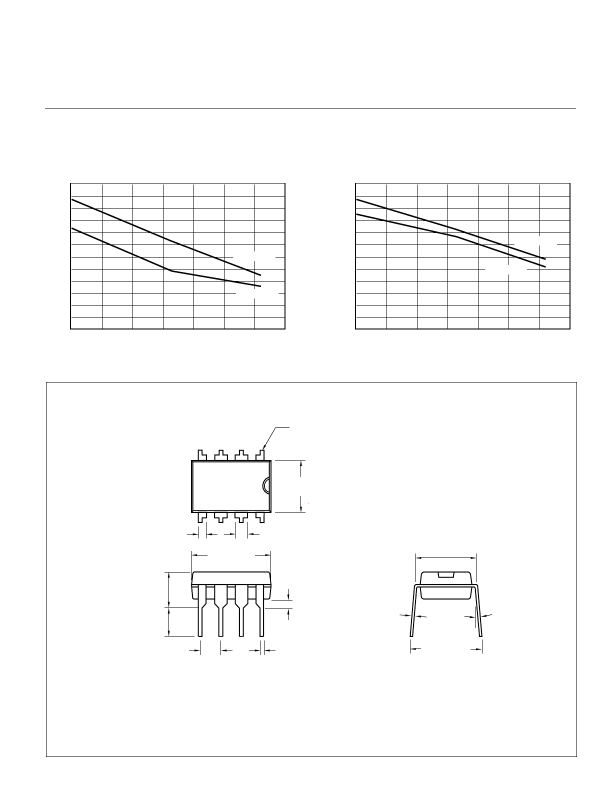
3
°
MIN.
PIN 1
.260 (6.60)
.240 (6.10)
.045 (1.14)
.030 (0.76)
.070 (1.78)
.040 (1.02)
.400 (10.16)
.348 (8.84)
.200 (5.08)
.140 (3.56)
.150 (3.81)
.115 (2.92)
.110 (2.79)
.090 (2.29)
.022 (0.56)
.015 (0.38)
.040 (1.02)
.020 (0.51)
.015 (0.38)
.008 (0.20)
.310 (7.87)
.290 (7.37)
.400 (10.16)
.310 (7.87)
PACKAGE DIMENSIONS
Unloaded Osc Freq vs. Temperature
12
10
0
2
4
6
8
-40
-20
0
20
40
100
60
80
OSCILLATOR FREQUENCY (kHz)
TEMPERATURE (
°
C)
V
IN
= 12V
V
IN
= 5V
Unloaded Osc Freq vs. Temperature
with Boost Pin = V
IN
60
50
0
10
20
30
40
-40
-20
0
20
40
100
60
80
OSCILLATOR FREQUENCY (kHz)
TEMPERATURE (
°
C)
V
IN
= 12V
V
IN
= 5V
8-Pin Plastic DIP
Dimensions: inches (mm)
Note: For the most current package drawings,
please see the Microchip Packaging Specification
located at http://www.microchip.com/packaging
10
TC7662B
CHARGE PUMP DC-TO-DC
VOLTAGE CONVERTER
TC7662B-8 9/11/96
© 2001 Microchip Technology Inc. DS21469A
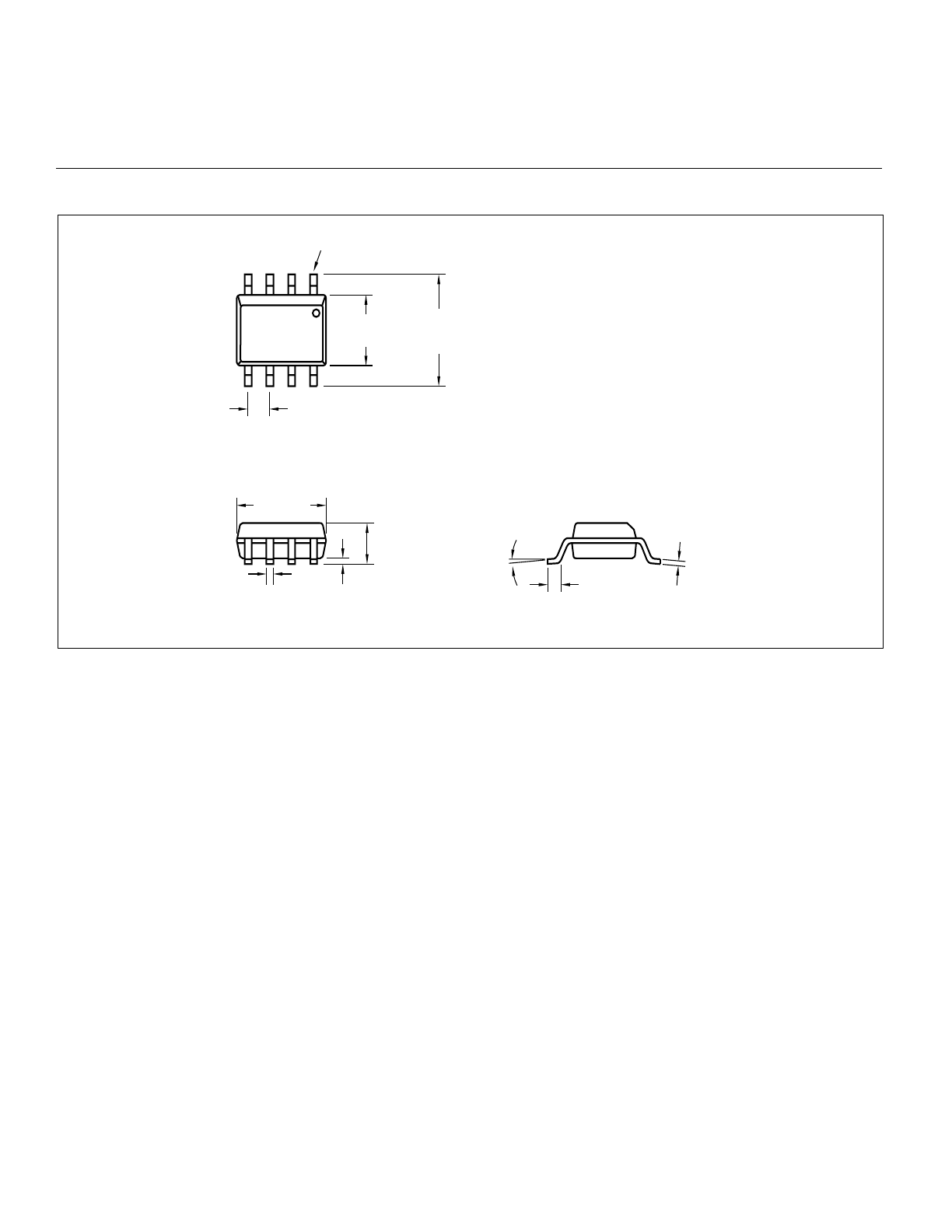
8-Pin SOIC
.050 (1.27) TYP.
8
°
MAX.
.244 (6.20)
.228 (5.79)
.157 (3.99)
.150 (3.81)
.197 (5.00)
.189 (4.80)
.020 (0.51)
.013 (0.33)
.010 (0.25)
.004 (0.10)
.069 (1.75)
.053 (1.35)
.010 (0.25)
.007 (0.18)
.050 (1.27)
.016 (0.40)
PACKAGE DIMENSIONS (Cont.)
Dimensions: inches (mm)
Note: For the most current package drawings,
please see the Microchip Packaging Specification
located at http://www.microchip.com/packaging