
2001-2015 Microchip Technology Inc.
DS20001467C-page 1
TC7660S
Features
• Oscillator boost from 10 kHz to 45 kHz
• Converts +5V Logic Supply to ±5V System
• Wide Input Voltage Range: +1.5V to +12V
• Efficient Voltage Conversion (99.9%, typical)
• Excellent Power Efficiency (98%, typical)
• Low Power Consumption: 80 µA (typical) @ V
IN
= 5V
• Low Cost and Easy to Use
- Only Two External Capacitors Required
• Available in 8-Pin Small Outline (SOIC) and 8-Pin
PDIP Packages
• Improved ESD Protection (10 kV HBM)
• No External Diode Required for High-Voltage
Operation
Applications
• RS-232 Negative Power Supply
• Simple Conversion of +5V to ±5V Supplies
• Voltage Multiplication V
OUT
= ± n V
+
• Negative Supplies for Data Acquisition Systems
and Instrumentation
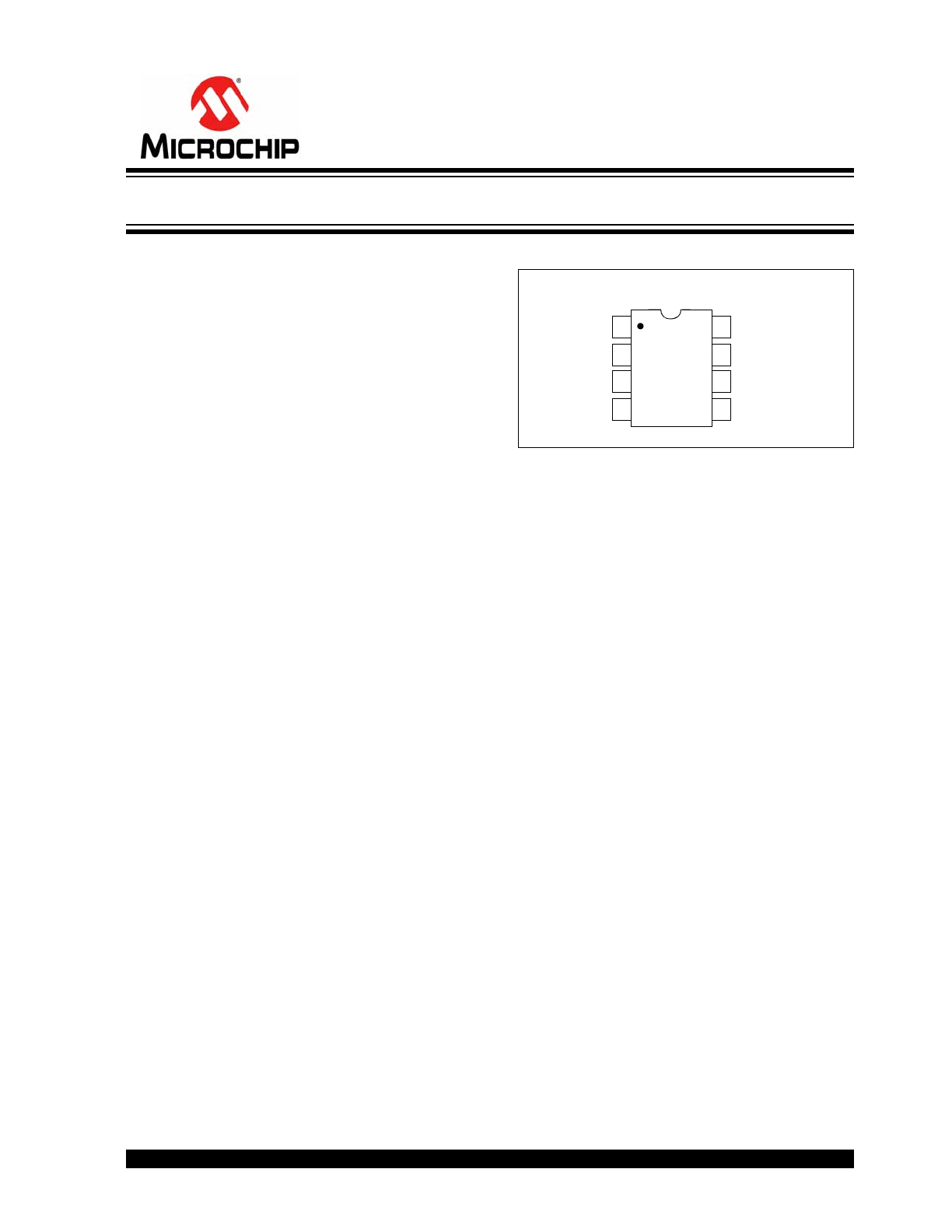
Package Types
General Description
The TC7660S device is a pin-compatible replacement
for the industry standard 7660 charge pump voltage
converter. It converts a +1.5V to +12V input to a corre-
sponding -1.5V to -12V output using only two low-cost
capacitors, eliminating inductors and their associated
cost, size and electromagnetic interference (EMI).
Added features include an extended supply range to
12V, and a frequency boost pin for higher operating fre-
quency, allowing the use of smaller external capacitors.
The on-board oscillator operates at a nominal fre-
quency of 10 kHz. Frequency is increased to 45 kHz
when pin 1 is connected to V
+
. Operation below 10 kHz
(for lower supply current applications) is possible by
connecting an external capacitor from OSC to ground
(with pin 1 open).
The TC7660S is available in 8-Pin PDIP and 8-Pin
Small Outline (SOIC) packages in commercial and
extended temperature ranges.
1
2
3
4
8
7
6
5
TC7660S
BOOST
CAP
+
GND
CAP
-
V
OUT
LOW
VOLTAGE (LV)
OSC
PDIP/SOIC
V
+
Super Charge Pump DC-to-DC Voltage Converter
TC7660S
DS20001467C-page 2
2001-2015 Microchip Technology Inc.
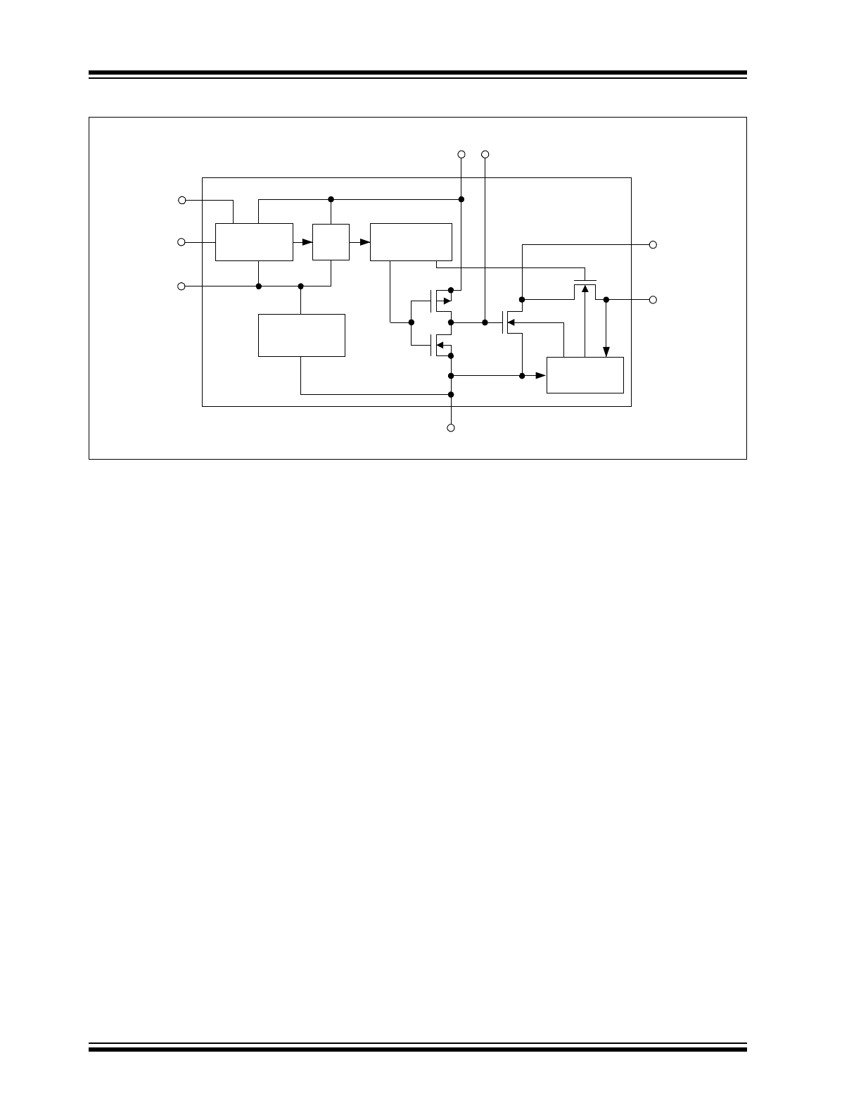
Functional Block Diagram
TC7660S
GND
Internal
Voltage
Regulator
RC
Oscillator
Voltage
Level
Translator
V
+
CAP
+
8
2
7
6
OSC
LV
3
Logic
Network
V
OUT
5
CAP-
4
2
Internal
Voltage
Regulator
BOOST
1
2001-2015 Microchip Technology Inc.
DS20001467C-page 3
TC7660S
1.0
ELECTRICAL
CHARACTERISTICS
Absolute Maximum Ratings†
Supply Voltage ................................................................+13V
LV, Boost, and OSC Inputs Voltage: (
Note 1
)
...................................-0.3V to (V
+
+ 0.3V) for V
+
< 5.5V
......................... (V
+
– 5.5V) to (V
+
+ 0.3V) for V
+
> 5.5V
Current into LV ......................................... 20 µA for V
+
> 3.5V
Output Short Duration (V
SUPPLY
5.5V)............... Continuous
Package Power Dissipation: (T
A
+70°C) (
Note 2
)
8-Pin PDIP ..........................................................730 mW
8-Pin SOIC..........................................................470 mW
Lead Temperature (Soldering, 10s) .... ....................... +300°C
Notice†:
Stresses above those listed under “Maximum
Ratings” may cause permanent damage to the device.
This is a stress rating only and functional operation of
the device at those or any other conditions above those
indicated in the operational sections of this
specification is not intended. Exposure to maximum
rating conditions for extended periods may affect
device reliability.
Note 1:
Connecting any input terminal to
voltages greater than V
+
or less than
GND may cause destructive latch-up. It
is recommended that no inputs from
sources operating from external
supplies be applied prior to “power up” of
the TC7660S.
2:
Derate linearly above +50°C by
5.5 mW/°C.
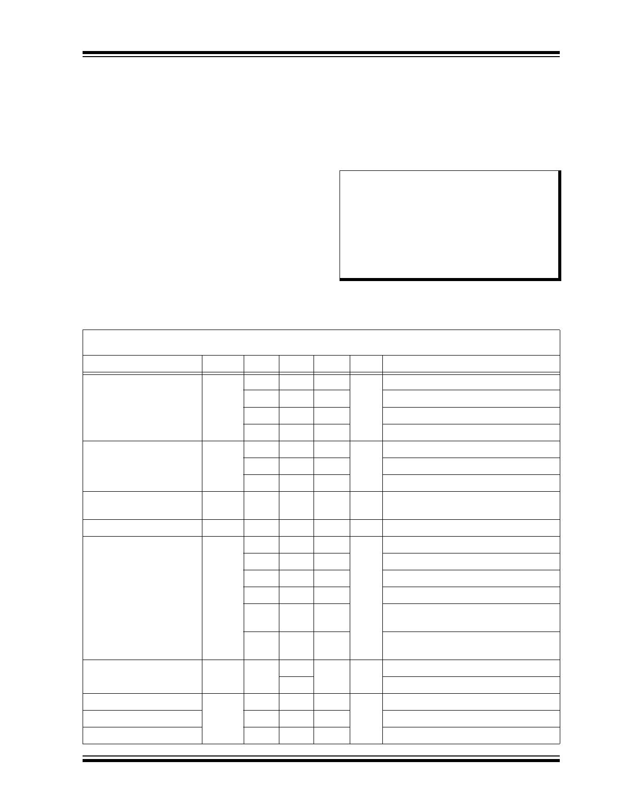
ELECTRICAL SPECIFICATIONS
Electrical Characteristics:
Unless otherwise noted, specifications measured over operating temperature range with
V
+
= 5V, C
OSC
= 0, refer to test circuit in
Figure 4-1
.
Parameters
Sym.
Min.
Typ.
Max.
Units
Conditions
Supply Current
(Boost pin OPEN or GND)
I
+
—
80
160
µA
R
L
=
—
—
180
0°C
T
A
+70°C
—
—
180
-40°C
T
A
+85°C
—
—
200
-55°C
T
A
+125°C
Supply Current
(Boost pin = V
+
)
I
+
—
—
300
µA
0°C
T
A
+70°C
—
—
350
-40°C
T
A
+85°C
—
—
400
-55°C
T
A
+125°C
Supply Voltage Range,
High
V
+
H
3.0
—
12
V
Min.
T
A
Max, R
L
= 10 k
, LV Open
Supply Voltage Range, Low
V
+
L
1.5
—
3.5
V
Min.
T
A
Max, R
L
= 10 k
, LV to GND
Output Source Resistance
R
OUT
—
60
100
I
OUT
= 20 mA
—
70
120
I
OUT
= 20 mA, 0°C
T
A
+70°C
—
70
120
I
OUT
= 20 mA, -40°C
T
A
+85°C
—
105
150
I
OUT
= 20 mA, -55°C
T
A
+125°C
—
—
250
V
+
= 2V, I
OUT
= 3 mA, LV to GND
0°C
T
A
+70°C
—
—
400
V
+
= 2V, I
OUT
= 3 mA, LV to GND
-55°C
T
A
+125°C
Oscillator Frequency
f
OSC
—
10
—
kHz
Pin 7 open, Pin 1 open or GND
45
Boost Pin = V
+
Power Efficiency
P
EFF
96
98
—
%
R
L
= 5 k
Boost Pin Open
95
98
—
T
MIN
T
A
T
MAX
; Boost Pin Open
—
88
—
Boost Pin = V
+
TC7660S
DS20001467C-page 4
2001-2015 Microchip Technology Inc.
Voltage Conversion
Efficiency
V
OUTEFF
99
99.9
—
%
R
L
=
Oscillator Impedance
Z
OSC
—
1
—
M
V
+
= 2V
—
100
—
k
V
+
= 5V
TEMPERATURE SPECIFICATIONS
Electrical Characteristics:
Unless otherwise noted, specifications measured over operating temperature range with
V
+
= 5V, C
OSC
= 0, refer to test circuit in
Figure 4-1
.
Parameters
Sym.
Min.
Typ.
Max.
Units
Conditions
Temperature Ranges
Operating Temperature Range
T
A
0
—
+70
°C
C suffix
T
A
-40
—
+85
°C
E suffix
T
A
-40
—
+125
°C
V suffix
Storage Temperature Range
T
A
-65
—
+150
°C
Thermal Package Resistances
Thermal Resistance, 8LD PDIP
JA
—
89.3
—
°C/W
Thermal Resistance, 8LD SOIC
JA
—
148.5
—
°C/W
ELECTRICAL SPECIFICATIONS (CONTINUED)
Electrical Characteristics:
Unless otherwise noted, specifications measured over operating temperature range with
V
+
= 5V, C
OSC
= 0, refer to test circuit in
Figure 4-1
.
Parameters
Sym.
Min.
Typ.
Max.
Units
Conditions
2001-2015 Microchip Technology Inc.
DS20001467C-page 5
TC7660S
2.0
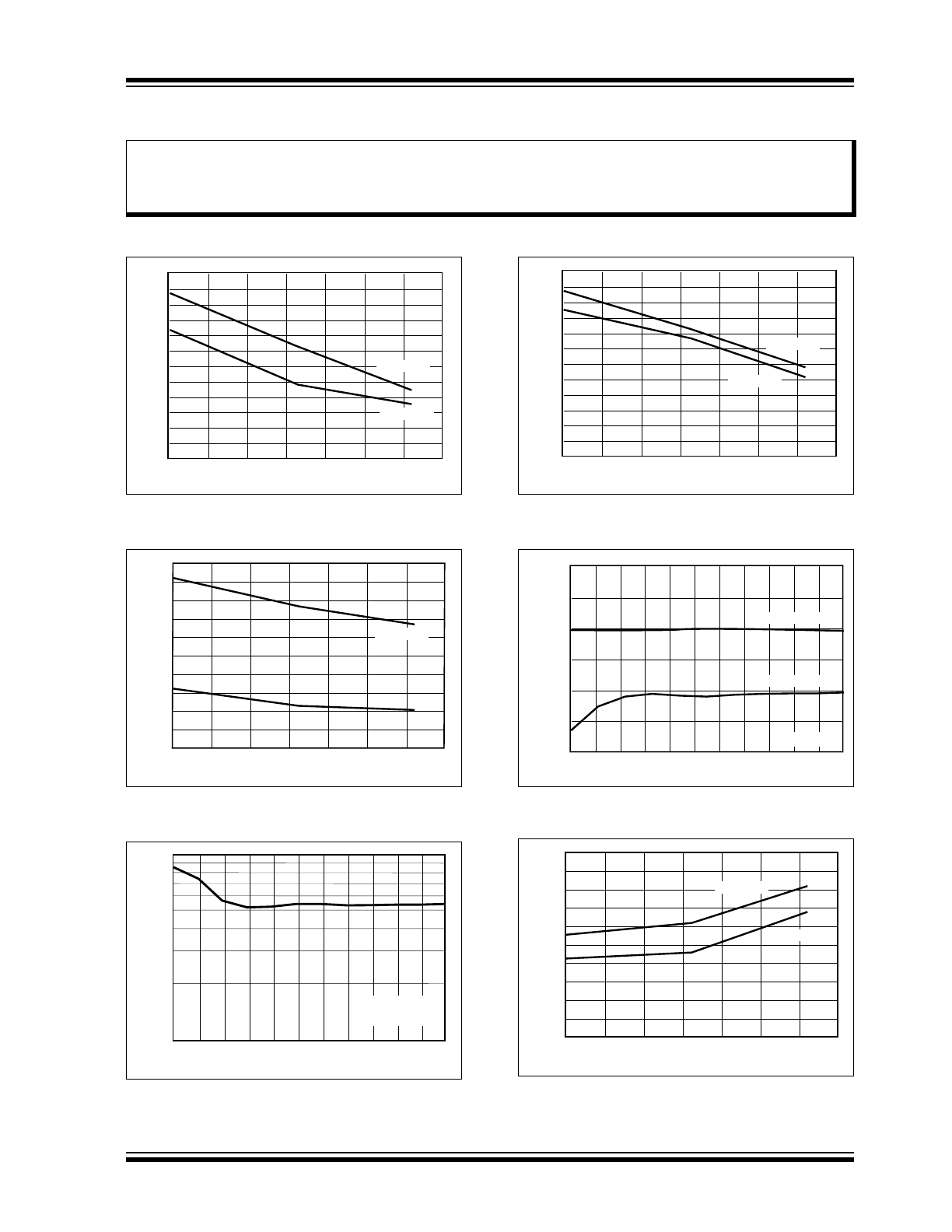
TYPICAL PERFORMANCE CURVES
Note:
Unless otherwise indicated, C
1
= C
2
= 10 µF, ESR
C1
= ESR
C2
= 1
, T
A
= 25°C. See
Figure 4-1
.
FIGURE 2-1:
Unloaded Oscillator
Frequency vs. Temperature.
FIGURE 2-2:
Supply Current vs.
Temperature (with Boost Pin = V
IN
).
FIGURE 2-3:
Output Source Resistance
vs. Supply Voltage.
FIGURE 2-4:
Unloaded Oscillator
Frequency vs. Temperature with Boost Pin = V
IN
.
FIGURE 2-5:
Voltage Conversion.
FIGURE 2-6:
Output Source Resistance
vs. Temperature.
Note:
The graphs and tables provided following this note are a statistical summary based on a limited number of
samples and are provided for informational purposes only. The performance characteristics listed herein
are not tested or guaranteed. In some graphs or tables, the data presented may be outside the specified
operating range (e.g., outside specified power supply range) and therefore outside the warranted range.
12
10
0
2
4
6
8
-40
-20
0
20
40
100
60
80
OSCILLATOR FREQUENCY (kHz)
TEMPERATURE (
°C)
V
IN
= 12V
V
IN
= 5V
1000
0
200
400
600
800
-40
-20
0
20
40
100
60
80
I
DD
(
μ
A)
TEMPERATURE (
°C)
V
IN
= 12V
V
IN
= 5V
I
OUT
= 20mA
T
A
= 25
°C
1.5
12
11.5
10.5
9.5
8.5
7.5
5.5 6.5
4.5
2.5 3.5
100
10
30
50
70
OUTPUT SOURCE RESISTANCE (
Ω
)
SUPPLY VOLTAGE (V)
IN
60
50
0
10
20
30
40
-40
-20
0
20
40
100
60
80
OSCILLATOR FREQUENCY (kHz)
TEMPERATURE (
°C)
V
IN
= 12V
V
IN
= 5V
Without Load
10K Load
101.0
100.5
100.0
99.5
99.0
98.5
98.0
1
12
11
10
9
8
7
5
6
4
2
3
VOLTAGE CONVERSION EFFICIENCY (%)
INPUT VOLTAGE V
IN
(V)
T
A
= 25
°C
100
0
20
40
60
80
-40
-20
0
20
40
100
60
80
OUTPUT SOURCE RESISTANCE (
Ω
)
TEMPERATURE (
°C)
V
IN
= 2.5V
V
IN
= 5.5V
TC7660S
DS20001467C-page 6
2001-2015 Microchip Technology Inc.
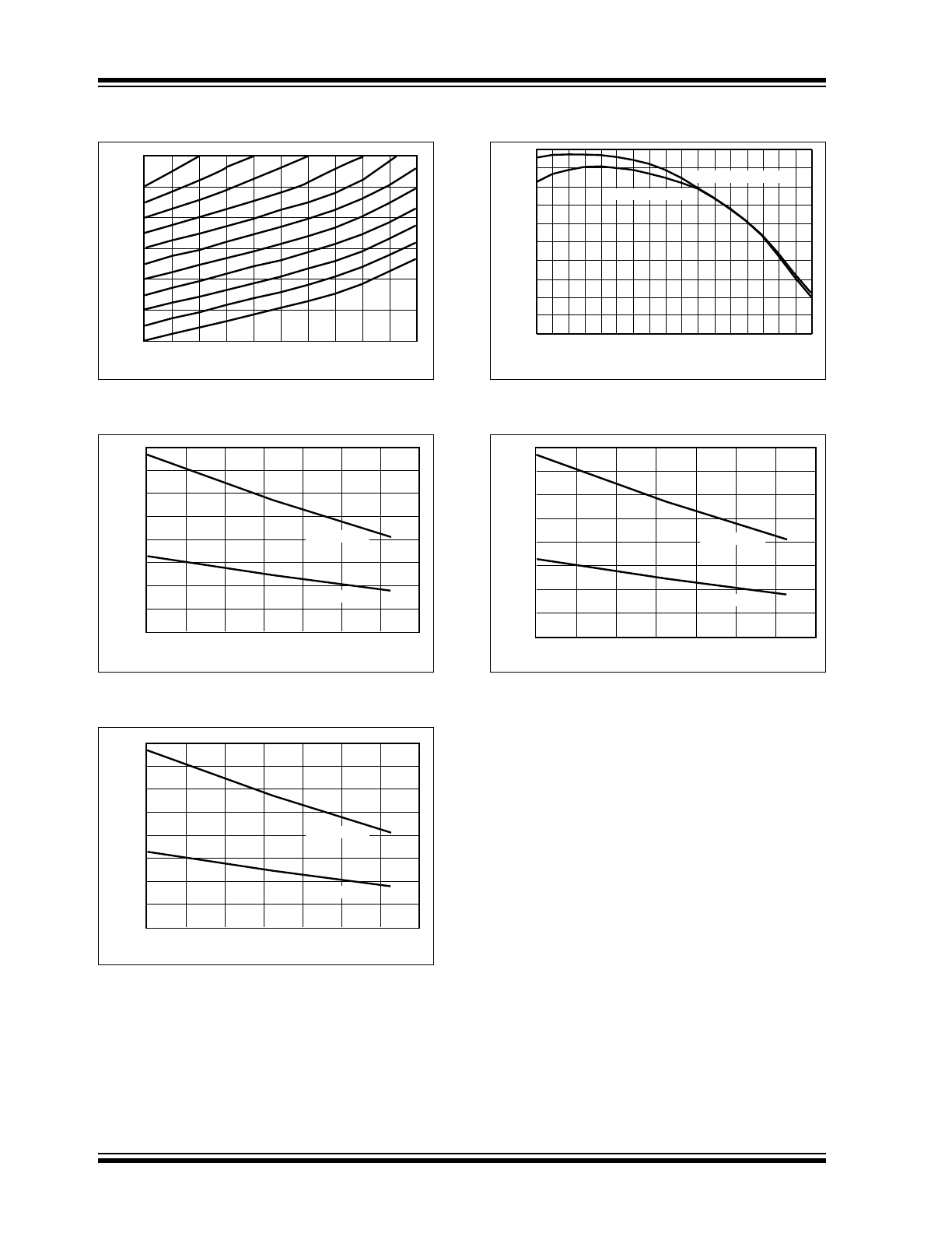
Note:
Unless otherwise indicated, C
1
= C
2
= 10 µF, ESR
C1
= ESR
C2
= 1
, T
A
= 25°C. See
Figure 4-1
.
FIGURE 2-7:
Output Voltage vs. Output
Current.
FIGURE 2-8:
Supply Current vs.
Temperature.
FIGURE 2-9:
Supply Current vs.
Temperature.
FIGURE 2-10:
Power Conversion
Efficiency vs. Load.
FIGURE 2-11:
Supply Current vs.
Temperature.
0
-2
-4
-6
-8
-10
-12
OUTPUT VOLTAGE V
OUT
(V)
OUTPUT CURRENT (mA)
0
100
90
80
70
60
40
50
30
10
20
200
150
125
175
100
75
50
25
0
SUPPLY CURRENT I
DD
(
μ
A)
TEMPERATURE (
°C)
-40
-20
0
20
40
100
60
80
V
IN
= 12.5V
V
IN
= 5.5V
200
150
125
175
100
75
50
25
0
SUPPLY CURRENT I
DD
(
μ
A)
TEMPERATURE (
°C)
-40
-20
0
20
40
100
60
80
V
IN
= 12.5V
V
IN
= 5.5V
POWER EFFICIENCY (%)
LOAD CURRENT (mA)
Boost Pin = Open
Boost Pin = V+
0
10
20
30
40
50
60
70
80
90
100
60.0
55.0
50.0
40.0
35.0
30.0
25.0
20.0
15.0
10.0
9.0
7.5
6.0
4.5
3.0
2.0
1.5
1.0
200
150
125
175
100
75
50
25
0
SUPPLY CURRENT I
DD
(
μ
A)
TEMPERATURE (
°C)
-40
-20
0
20
40
100
60
80
V
IN
= 12.5V
V
IN
= 5.5V
2001-2015 Microchip Technology Inc.
DS20001467C-page 7
TC7660S
3.0
PIN DESCRIPTIONS
The descriptions of the pins are listed in
Table 3-1
.
3.1
Switching Frequency Boost Pin
(Boost)
By connecting the boost pin (pin 1), the switching
frequency of the charge pump is increased from 10 kHz
typical to 45 kHz typical. By connecting the boost pin
(pin1), to the V
+
pin (pin 8), the switching frequency of
the charge pump is increased from 10 kHz typical to
45 kHz typical.
3.2
Charge Pump Capacitor (CAP
+
)
Positive connection for the charge pump capacitor, or
flying capacitor, used to transfer charge from the input
source to the output. In the voltage-inverting
configuration, the charge pump capacitor is charged to
the input voltage during the first half of the switching
cycle. During the second half of the switching cycle, the
charge pump capacitor is inverted and charge is
transferred to the output capacitor and load.
It is recommended that a low ESR (equivalent series
resistance) capacitor be used. Additionally, larger
values will lower the output resistance.
3.3
Ground (GND)
Input and output zero volt reference.
3.4
Charge Pump Capacitor (CAP
-
)
Negative connection for the charge pump capacitor, or
flying capacitor, used to transfer charge from the input
to the output. Proper orientation is imperative when
using a polarized capacitor.
3.5
Output Voltage (V
OUT
)
Negative connection for the charge pump output
capacitor. In the voltage-inverting configuration, the
charge pump output capacitor supplies the output load
during the first half of the switching cycle. During the
second half of the switching cycle, charge is restored to
the charge pump output capacitor.
It is recommended that a low ESR capacitor be used.
Additionally, larger values will lower the output ripple.
3.6
Low Voltage Pin (LV)
The low voltage pin ensures proper operation of the
internal oscillator for input voltages below 3.5V. The low
voltage pin should be connected to ground (GND) for
input voltages below 3.5V. Otherwise, the low voltage
pin should be allowed to float.
3.7
Oscillator Control Input (OSC)
The oscillator control input can be utilized to slow down
or speed up the operation of the TC7660S. Refer to
Section 5.4 “Changing the TC7660S Oscillator
Frequency”
, for details on altering the oscillator
frequency.
3.8
Power Supply (V
+
)
Positive power supply input voltage connection. It is
recommended that a low ESR capacitor be used to
bypass the power supply input to ground (GND).
TABLE 3-1:
PIN FUNCTION TABLE
Pin No.
Symbol
Description
1
BOOST
Switching Frequency boost pin
2
CAP
+
Charge pump capacitor positive terminal
3
GND
Ground terminal
4
CAP
-
Charge pump capacitor negative terminal
5
V
OUT
Output voltage
6
LV
Low voltage pin. Connect to GND for V+ < 3.5V
7
OSC
Oscillator control input. Bypass with an external capacitor to slow the oscillator.
8
V
+
Power supply positive voltage input
TC7660S
DS20001467C-page 8
2001-2015 Microchip Technology Inc.
4.0
DETAILED DESCRIPTION
4.1
Theory of Operation
The TC7660S contains all the necessary circuitry to
implement a voltage inverter, with the exception of two
external capacitors, which may be inexpensive 10 µF
polarized electrolytic capacitors. Operation is best
understood by considering
Figure 4-2
, which shows an
idealized voltage inverter. Capacitor C
1
is charged to a
voltage V
+
for the half cycle when switches S
1
and S
3
are closed. (Note that switches S
2
and S
4
are open
during this half cycle.) During the second half cycle of
operation, switches S
2
and S
4
are closed, with S
1
and
S
3
open, thereby shifting capacitor C
1
negatively by V
+
volts. Charge is then transferred from C
1
negatively by
V
+
volts. Charge is then transferred from C
1
to C
2
, such
that the voltage on C
2
is exactly V
+
assuming ideal
switches and no load on C
2
.
The four switches in
Figure 4-2
are MOS power
switches; S
1
is a P-channel device, and S
2
, S
3
and S
4
are N-channel devices. The main difficulty with this
approach is that in integrating the switches, the sub-
strates of S
3
and S
4
must always remain
reverse-biased with respect to their sources, but not so
much as to degrade their ON resistances. In addition,
at circuit start-up, and under output short circuit condi-
tions (V
OUT
= V
+
), the output voltage must be sensed
and the substrate bias adjusted accordingly. Failure to
accomplish this will result in high power losses and
probable device latch-up.
This problem is eliminated in the TC7660S by a logic
network which senses the output voltage (V
OUT
)
together with the level translators, and switches the
substrates of S
3
and S
4
to the correct level to maintain
necessary reverse bias.
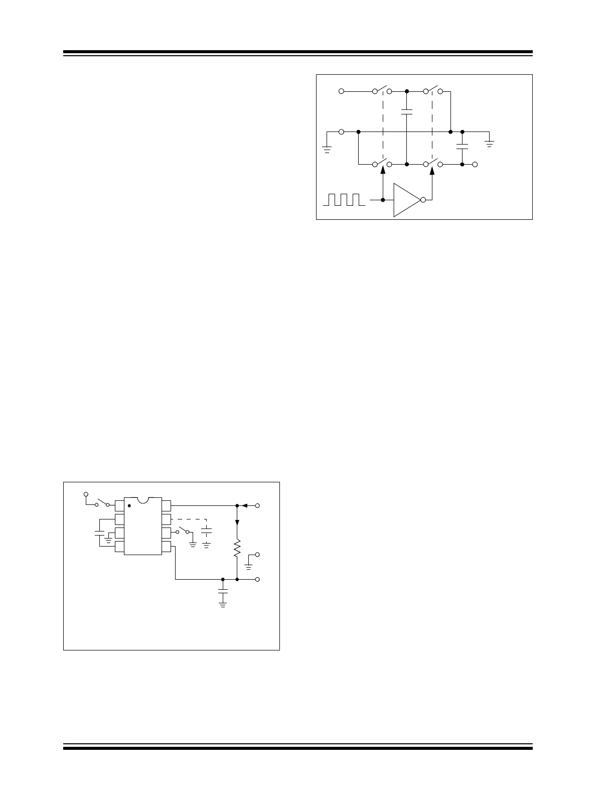
FIGURE 4-1:
TC7660S Test Circuit.
The voltage regulator portion of the TC7660S is an
integral part of the anti-latch-up circuitry. Its inherent
voltage drop can, however, degrade operation at low
voltages.
FIGURE 4-2:
Ideal Charge Pump Inverter.
To improve low-voltage operation, the “LV” pin should
be connected to GND, disabling the regulator. For
supply voltages greater than 3.5V, the LV terminal must
be left open to ensure latch-up-proof operation and
prevent device damage.
4.2
Theoretical Power Efficiency
Considerations
In theory, a capacitive charge pump can approach
100% efficiency if certain conditions are met:
(1) The drive circuitry consumes minimal power.
(2) The output switches have extremely low ON
resistance and virtually no offset.
(3) The impedances of the pump and reservoir
capacitors are negligible at the pump frequency.
The TC7660S approaches these conditions for nega-
tive voltage multiplication if large values of C
1
and C
2
are used. Energy is lost only in the transfer of charge
between capacitors if a change in voltage occurs. The
energy lost is defined by:
E = 1/2 C
1
(V
1
2
– V
2
2
)
V
1
and V
2
are the voltages on C
1
during the pump and
transfer cycles. If the impedances of C
1
and C
2
are rel-
atively high at the pump frequency (refer to
Figure 4-2
)
compared to the value of R
L
, there will be a substantial
difference in voltages V
1
and V
2
. Therefore, it is desir-
able not only to make C
2
as large as possible to
eliminate output voltage ripple, but also to employ a
correspondingly large value for C
1
in order to achieve
maximum efficiency of operation.
4.3
Dos and Don'ts
• Do not exceed maximum supply voltages.
• Do not connect the LV terminal to GND for supply
voltages greater than 3.5V.
• Do not short circuit the output to V
+
supply for
voltages above 5.5V for extended periods; how-
ever, transient conditions including start-up are
okay.
• When using polarized capacitors in the inverting
mode, the + terminal of C
1
must be connected to
pin 2 of the TC7660S and the + terminal of C
2
must be connected to GND.
1
2
3
4
8
7
6
5
TC7660S
+
V
+
(+5V)
V
OUT
C
1
10 µF
C
OSC
+
C
2
10 µF
I
L
R
L
I
S
V
+
Note:
For large values of C
OSC
(>1000 pF), the
values of C
1
and C
2
should be increased to
100F.
V
+
GND S
3
S
1
S
2
S
4
C
2
V
OUT
= -V
IN
C
1
+
+
2001-2015 Microchip Technology Inc.
DS20001467C-page 9
TC7660S
5.0
APPLICATIONS INFORMATION
5.1
Simple Negative Voltage
Converter
Figure 5-1
shows typical connections to provide a
negative supply where a positive supply is available. A
similar scheme may be employed for supply voltages
anywhere in the operating range of +1.5V to +12V,
keeping in mind that pin 6 (LV) is tied to the supply
negative (GND) only for supply voltages below 3.5V.
FIGURE 5-1:
Simple Negative Converter.
The output characteristics of the circuit in
Figure 5-1
are those of a nearly ideal voltage source in series with
a 70
resistor. Thus, for a load current of -10 mA and
a supply voltage of +5V, the output voltage would be
-4.3V.
The dynamic output impedance of the TC7660S is due,
primarily, to capacitive reactance of the charge transfer
capacitor (C
1
). Since this capacitor is connected to the
output for only half of the cycle, the equation is:
EQUATION
5.2
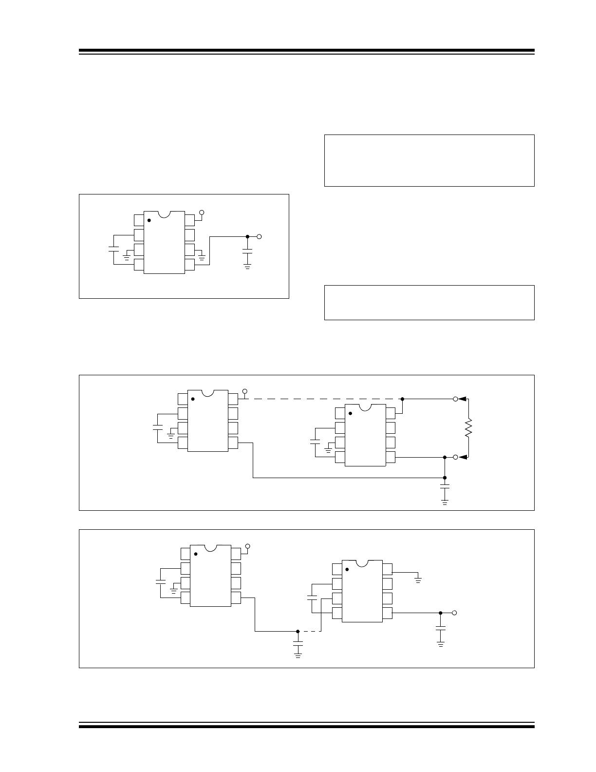
Paralleling Devices
Any number of TC7660S voltage converters may be
paralleled to reduce output resistance (
Figure 5-2
). The
reservoir capacitor, C
2
, serves all devices, while each
device requires its own pump capacitor, C
1
. The resul-
tant output resistance would be approximately:
EQUATION
FIGURE 5-2:
Paralleling Devices Lowers Output Impedance.
FIGURE 5-3:
Increased Output Voltage By Cascading Devices.
+
V
+
+
1
2
3
4
8
7
6
5
TC7660S
V
OUT
*
C
1
10 µF
* V
OUT
= -V
+
for 1.5V
V+ 12V
C
2
10 µF
X
C
2
2fC
1
-----------
3.18
=
=
where:
f = 10 kHz and C1 = 10 µF.
R
OUT
R
OUT
of TC7660S
n number of devices
---------------------------------------------------
=
“n”
“1”
R
L
+
V
+
+
1
2
3
4
8
7
6
5
TC7660S
C
1
C
2
+
1
2
3
4
8
7
6
5
TC7660S
C
1
V
OUT
*
“1”
+
V
+
+
1
2
3
4
8
7
6
5
TC7660S
10 µF
*
V
OUT
= -n V
+
for 1.5V
V+ 12V
“n”
+
1
2
3
4
8
7
6
5
TC7660S
10 µF
10 µF
+
10 µF
TC7660S
DS20001467C-page 10
2001-2015 Microchip Technology Inc.
5.3
Cascading Devices
The TC7660S may be cascaded as shown (
Figure 5-3
)
to produce larger negative multiplication of the initial
supply voltage. However, due to the finite efficiency of
each device, the practical limit is 10 devices for light
loads. The output voltage is defined by:
EQUATION
where n is an integer representing the number of
devices cascaded. The resulting output resistance
would be approximately the weighted sum of the
individual TC7660S R
OUT
values.
5.4
Changing the TC7660S Oscillator
Frequency
It may be desirable in some applications (due to noise
or other considerations) to increase the oscillator fre-
quency. Pin 1, frequency boost pin, may be connected
to V
+
to increase oscillator frequency to 45 kHz from a
nominal of 10 kHz for an input supply voltage of 5.0V.
The oscillator may also be synchronized to an external
clock as shown in
Figure 5-4
. In order to prevent possi-
ble device latch-up, a 1 kΩ resistor must be used in
series with the clock output. In a situation where the
designer has generated the external clock frequency
using TTL logic, the addition of a 10 kΩ pull-up resistor
to V
+
supply is required. Note that the pump frequency
with external clocking, as with internal clocking, will be
half of the clock frequency. Output transitions occur on
the positive-going edge of the clock.
FIGURE 5-4:
External Clocking.
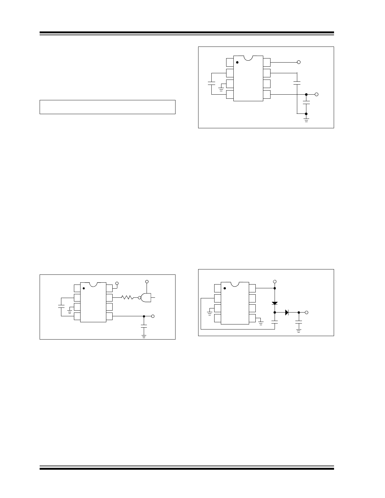
It is also possible to increase the conversion efficiency
of the TC7660S at low load levels by lowering the
oscillator frequency. This reduces the switching losses,
and is achieved by connecting an additional capacitor,
C
OSC
, as shown in
Figure 5-5
. Lowering the oscillator
frequency will cause an undesirable increase in the
impedance of the pump (C
1
) and the reservoir (C
2
)
capacitors. To overcome this, increase the values of C
1
and C
2
by the same factor that the frequency has been
reduced. For example, the addition of a 100 pF
capacitor between pin 7 (OSC) and pin 8 (V
+
) will lower
the oscillator frequency to 1 kHz from its nominal
frequency of 10 kHz (a multiple of 10), and necessitate
a corresponding increase in the values of C
1
and C
2
(from 10 µF to 100 µF).
FIGURE 5-5:
Lowering Oscillator
Frequency.
5.5
Positive Voltage Multiplication
The TC7660S may be employed to achieve positive
voltage multiplication using the circuit shown in
Figure 5-6
. In this application, the pump inverter
switches of the TC7660S are used to charge C
1
to a
voltage level of V
+
–V
F
(where V
+
is the supply voltage
and V
F
is the forward voltage drop of diode D
1
). On the
transfer cycle, the voltage on C
1
plus the supply voltage
(V
+
) is applied through diode D
2
to capacitor C
2
. The
voltage thus created on C
2
becomes (2V
+
) – (2V
F
), or
twice the supply voltage minus the combined forward
voltage drops of diodes D
1
and D
2.
The source impedance of the output (V
OUT
) will depend
on the output current, but for V
+
= 5V and an output
current of 10 mA, it will be approximately 60Ω.
FIGURE 5-6:
Positive Voltage Multiplier.
V
OUT
n
–
V
+
=
CMOS
GATE
1 k
V
OUT
“1”
+
V
+
+
1
2
3
4
8
7
6
5
TC7660S
10 µF
10 µF
V
+
V
OUT
+
+
1
2
3
4
8
7
6
5
TC7660S
C
1
C
2
V
+
C
OSC
+
C
2
D
1
D
2
+
C
1
V
OUT
=
1
2
3
4
8
7
6
5
TC7660S
V
+
(2 V
+
) - (2 V
F
)