
2002-2011 Microchip Technology Inc.
DS21465C-page 1
TC7660
Features
• Wide Input Voltage Range: +1.5V to +10V
• Efficient Voltage Conversion (99.9%, typ)
• Excellent Power Efficiency (98%, typ)
• Low Power Consumption: 80 µA (typ) @ V
IN
= 5V
• Low Cost and Easy to Use
- Only Two External Capacitors Required
• Available in 8-Pin Small Outline (SOIC), 8-Pin
PDIP and 8-Pin CERDIP Packages
• Improved ESD Protection (3 kV HBM)
• No External Diode Required for High-Voltage
Operation
Applications
• RS-232 Negative Power Supply
• Simple Conversion of +5V to ±5V Supplies
• Voltage Multiplication V
OUT
= ± n V
+
• Negative Supplies for Data Acquisition Systems
and Instrumentation
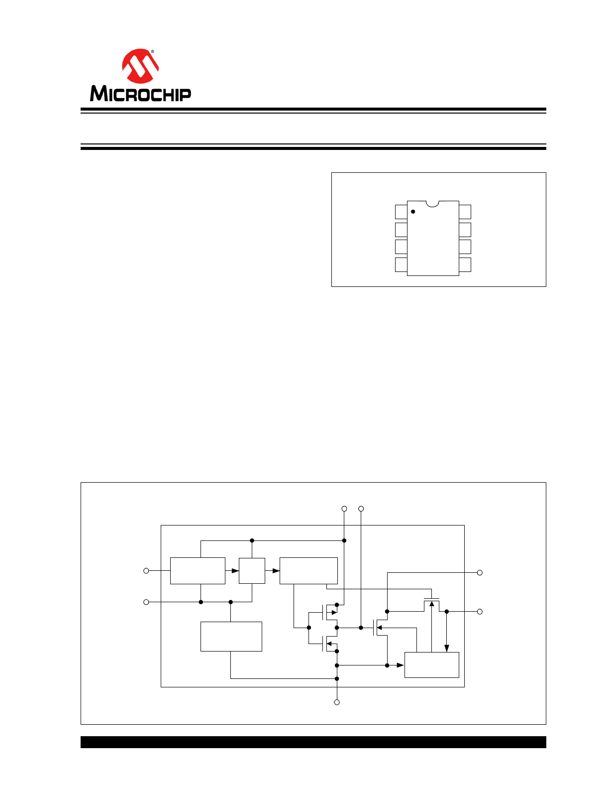
Package Types
General Description
The TC7660 device is a pin-compatible replacement
for the industry standard 7660 charge pump voltage
converter. It converts a +1.5V to +10V input to a corre-
sponding -1.5V to -10V output using only two low-cost
capacitors, eliminating inductors and their associated
cost, size and electromagnetic interference (EMI).
The on-board oscillator operates at a nominal fre-
quency of 10 kHz. Operation below 10 kHz (for lower
supply current applications) is possible by connecting
an external capacitor from OSC to ground.
The TC7660 is available in 8-Pin PDIP, 8-Pin Small
Outline (SOIC) and 8-Pin CERDIP packages in
commercial and extended temperature ranges.
Functional Block Diagram
1
2
3
4
8
7
6
5
TC7660
NC
CAP
+
GND
CAP
-
V
OUT
LOW
VOLTAGE (LV)
OSC
PDIP/CERDIP/SOIC
V
+
TC7660
GND
Internal
Voltage
Regulator
RC
Oscillator
Voltage
Level
Translator
V
+
CAP
+
8
2
7
6
OSC
LV
3
Logic
Network
V
OUT
5
CAP-
4
2
Internal
Voltage
Regulator
Charge Pump DC-to-DC Voltage Converter
TC7660
DS21465C-page 2
2002-2011 Microchip Technology Inc.
1.0
ELECTRICAL
CHARACTERISTICS
Absolute Maximum Ratings*
Supply Voltage .............................................................+10.5V
LV and OSC Inputs Voltage: (
Note 1
)
.............................................. -0.3V to V
SS
for V
+
< 5.5V
..................................... (V
+
– 5.5V) to (V
+
) for V
+
> 5.5V
Current into LV ......................................... 20 µA for V
+
> 3.5V
Output Short Duration (V
SUPPLY
5.5V)...............Continuous
Package Power Dissipation: (T
A
70°C)
8-Pin CERDIP ....................................................800 mW
8-Pin PDIP .........................................................730 mW
8-Pin SOIC .........................................................470 mW
Operating Temperature Range:
C Suffix.......................................................0°C to +70°C
I Suffix .....................................................-25°C to +85°C
E Suffix....................................................-40°C to +85°C
M Suffix .................................................-55°C to +125°C
Storage Temperature Range .........................-65°C to +160°C
ESD protection on all pins (HBM) .................................
3 kV
Maximum Junction Temperature ........... ....................... 150°C
* Notice: Stresses above those listed under “Maximum Rat-
ings” may cause permanent damage to the device. This is a
stress rating only and functional operation of the device at
those or any other conditions above those indicated in the
operational sections of this specification is not intended. Expo-
sure to maximum rating conditions for extended periods may
affect device reliability.
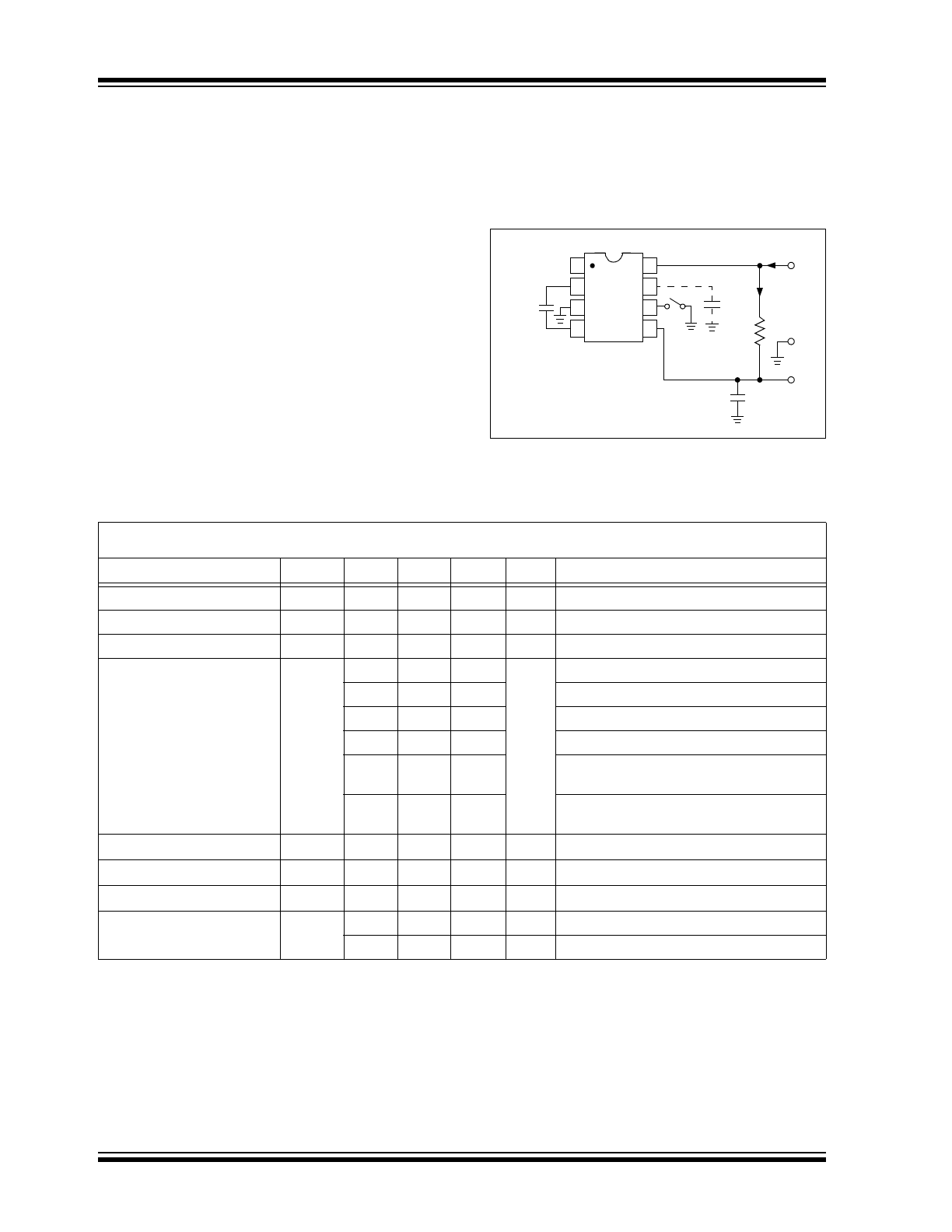
FIGURE 1-1:
TC7660 Test Circuit.
ELECTRICAL SPECIFICATIONS
1
2
3
4
8
7
6
5
TC7660
+
V
+
(+5V)
V
OUT
C
1
10 µF
C
OSC
+
C
2
10 µF
I
L
R
L
I
S
Electrical Characteristics: Unless otherwise noted, specifications measured over operating temperature range with V
+
= 5V,
C
OSC
= 0, refer to test circuit in
Figure 1-1
.
Parameters
Sym
Min
Typ
Max
Units
Conditions
Supply Current
I
+
—
80
180
µA
R
L
=
Supply Voltage Range, High
V
+
H
3.0
—
10
V
Min
T
A
Max, R
L
= 10 k
, LV Open
Supply Voltage Range, Low
V
+
L
1.5
—
3.5
V
Min
T
A
Max, R
L
= 10 k
, LV to GND
Output Source Resistance
R
OUT
—
70
100
I
OUT
=20 mA, T
A
= +25°C
—
—
120
I
OUT
=20 mA, T
A
+70°C (C Device)
—
—
130
I
OUT
=20 mA, T
A
+85°C (E and I Device)
—
104
150
I
OUT
=20 mA, T
A
+125°C (M Device)
—
150
300
V
+
= 2V, I
OUT
= 3 mA, LV to GND
0°C
T
A
+70°C
—
160
600
V
+
= 2V, I
OUT
= 3 mA, LV to GND
-55°C
T
A
+125°C (M Device)
Oscillator Frequency
f
OSC
—
10
—
kHz
Pin 7 open
Power Efficiency
P
EFF
95
98
—
%
R
L
= 5 k
Voltage Conversion Efficiency
V
OUTEFF
97
99.9
—
%
R
L
=
Oscillator Impedance
Z
OSC
—
1.0
—
M
V
+
= 2V
—
100
—
k
V
+
= 5V
Note 1: Destructive latch-up may occur if voltages greater than V
+
or less than GND are supplied to any input pin.
2002-2011 Microchip Technology Inc.
DS21465C-page 3
TC7660
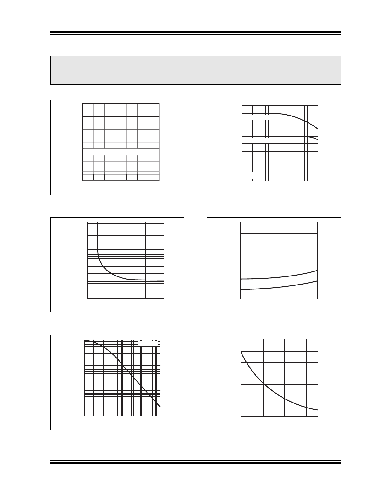
2.0
TYPICAL PERFORMANCE CURVES
Note: Unless otherwise indicated, C
1
= C
2
= 10 µF, ESR
C1
= ESR
C2
= 1
, T
A
= 25°C. See
Figure 1-1
.
FIGURE 2-1:
Operating Voltage vs.
Temperature.
FIGURE 2-2:
Output Source Resistance
vs. Supply Voltage.
FIGURE 2-3:
Frequency of Oscillation vs.
Oscillator Capacitance.
FIGURE 2-4:
Power Conversion
Efficiency vs. Oscillator Frequency.
FIGURE 2-5:
Output Source Resistance
vs. Temperature.
FIGURE 2-6:
Unloaded Oscillator
Frequency vs. Temperature.
Note:
The graphs and tables provided following this note are a statistical summary based on a limited number of
samples and are provided for informational purposes only. The performance characteristics listed herein
are not tested or guaranteed. In some graphs or tables, the data presented may be outside the specified
operating range (e.g., outside specified power supply range) and therefore outside the warranted range.
-25
0
+25
+75 +100 +125
12
10
8
6
4
2
+50
-55
SUPPLY VOLTAGE (V)
TEMPERATURE (
°C)
0
SUPPLY VOLTAGE RANGE
7
8
10k
1k
100
Ω
OUTPUT SOURCE RESISTANCE (
Ω
)
6
5
4
3
2
1
0
SUPPLY VOLTAGE (V)
10
Ω
OSCILLATOR CAPACITANCE (pF)
10k
OSCILLATOR FREQUENCY (Hz)
1
1k
100
10
10
100
1000
10k
V+ = +5V
OSCILLATOR FREQUENCY (Hz)
100
POWER CONVERSION EFFICIENCY (%)
98
96
92
90
88
86
84
82
80
94
100
1k
10k
V+ = +5V
I
OUT
= 1 mA
I
OUT
= 15 mA
500
450
400
200
150
100
50
0
-55
-25
0
+25
+50
+75 +100 +125
TEMPERATURE (
°C)
OUTPUT SOURCE RESISTANCE (
Ω
)
V + = +2V
V + = +5V
I
OUT
= 1 mA
TEMPERATURE (
°C)
OSCILLATOR FREQUENCY (kHz)
20
-55
18
16
14
12
10
8
6
-25
0
+25 +50
+75 +100 +125
V+ = +5V
TC7660
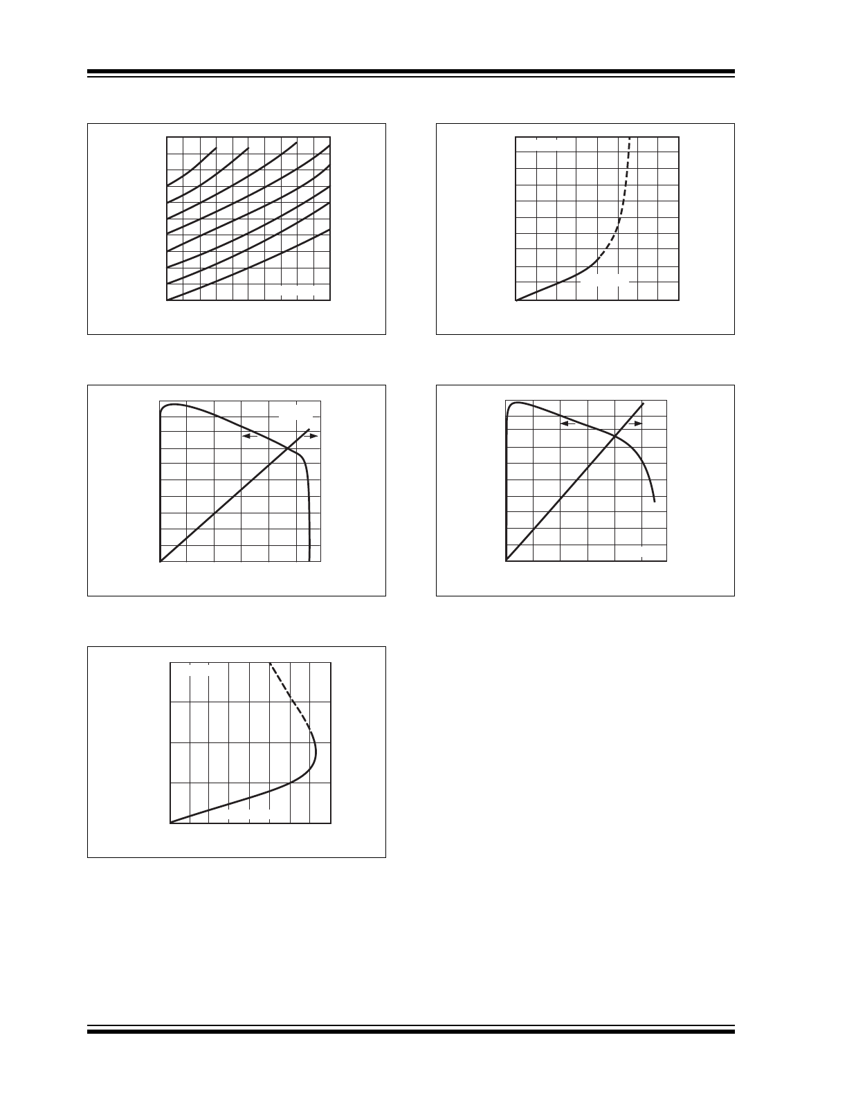
DS21465C-page 4
2002-2011 Microchip Technology Inc.
Note: Unless otherwise indicated, C
1
= C
2
= 10 µF, ESR
C1
= ESR
C2
= 1
, T
A
= 25°C. See
Figure 1-1
.
FIGURE 2-7:
Output Voltage vs. Output
Current.
FIGURE 2-8:
Supply Current and Power
Conversion Efficiency vs. Load Current.
FIGURE 2-9:
Output Voltage vs. Load
Current.
FIGURE 2-10:
Output Voltage vs. Load
Current.
FIGURE 2-11:
Supply Current and Power
Conversion Efficiency vs. Load Current.
OUTPUT CURRENT (mA)
OUTPUT VOLTAGE (V)
0
0
-1
-2
-3
-4
-5
-6
-7
-8
-9
-10
10
20 30 40 50
60 70 80
90 100
LV OPEN
POWER CONVERSION EFFICIENCY (%)
0
LOAD CURRENT (mA)
10
20
30
40
50
60
70
80
90
100
1.5
3.0
4.5
6.0
7.5
9.0
0
2
4
6
8
10
12
14
16
18
20
SUPPLY CURRENT (mA)
V+ = 2V
2
0
OUTPUT VOLTAGE (V)
1
0
-1
-2
1
2
3
4
5
6
7
8
LOAD CURRENT (mA)
SLOPE 150
Ω
V+ = +2V
LOAD CURRENT (mA)
OUTPUT VOLTAGE (V)
1
0
5
4
3
2
0
-1
-2
-3
-4
-5
10
20
30
40
50
60
70
80
V+ = +5V
SLOPE 55
Ω
LOAD CURRENT (mA)
POWER CONVERSION EFFICIENCY (%)
0
10
20
30
40
50
60
70
80
90
100
0
10
20
30
40
50
60
70
80
90
100
SUPPLY CURRENT (mA)
10
20
30
40
50
60
V+ = +5V
2002-2011 Microchip Technology Inc.
DS21465C-page 5
TC7660
3.0
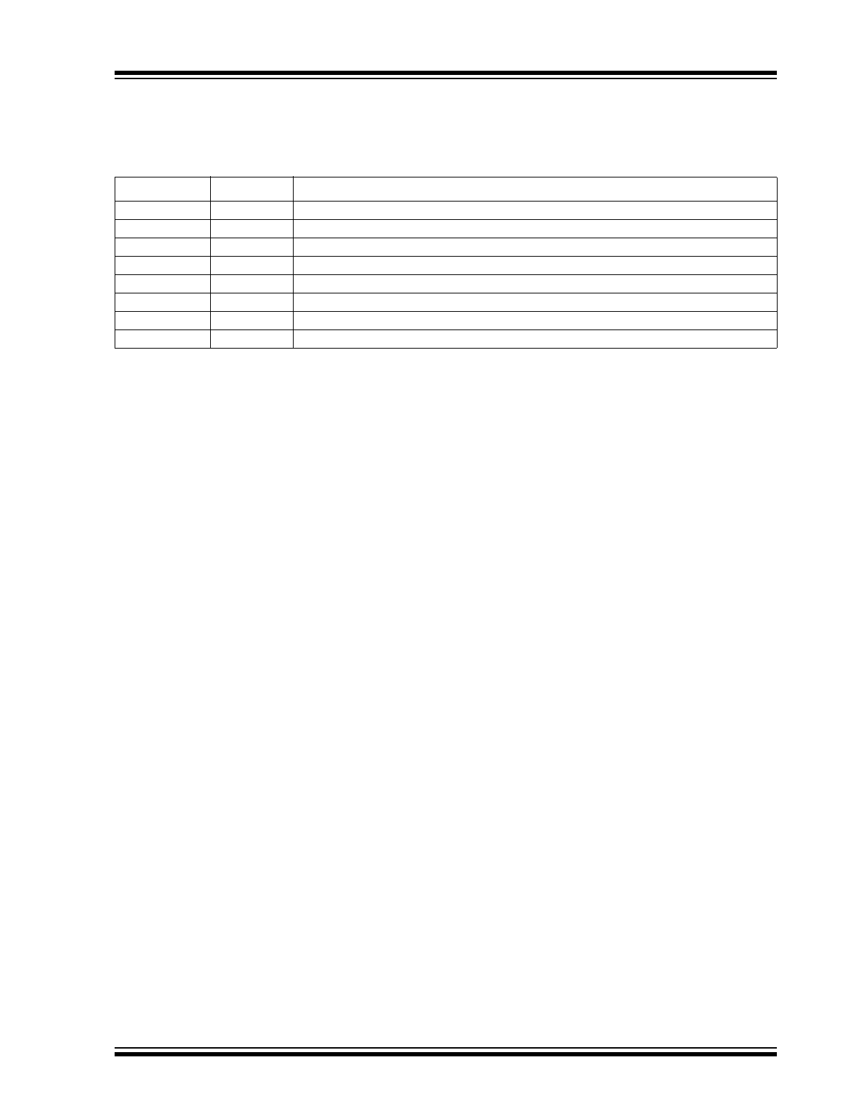
PIN DESCRIPTIONS
The descriptions of the pins are listed in
Table 3-1
.
TABLE 3-1:
PIN FUNCTION TABLE
3.1
Charge Pump Capacitor (CAP
+
)
Positive connection for the charge pump capacitor, or
flying capacitor, used to transfer charge from the input
source to the output. In the voltage-inverting configura-
tion, the charge pump capacitor is charged to the input
voltage during the first half of the switching cycle. Dur-
ing the second half of the switching cycle, the charge
pump capacitor is inverted and charge is transferred to
the output capacitor and load.
It is recommended that a low ESR (equivalent series
resistance) capacitor be used. Additionally, larger
values will lower the output resistance.
3.2
Ground (GND)
Input and output zero volt reference.
3.3
Charge Pump Capacitor (CAP
-
)
Negative connection for the charge pump capacitor, or
flying capacitor, used to transfer charge from the input
to the output. Proper orientation is imperative when
using a polarized capacitor.
3.4
Output Voltage (V
OUT
)
Negative connection for the charge pump output
capacitor. In the voltage-inverting configuration, the
charge pump output capacitor supplies the output load
during the first half of the switching cycle. During the
second half of the switching cycle, charge is restored to
the charge pump output capacitor.
It is recommended that a low ESR (equivalent series
resistance) capacitor be used. Additionally, larger
values will lower the output ripple.
3.5
Low Voltage Pin (LV)
The low voltage pin ensures proper operation of the
internal oscillator for input voltages below 3.5V. The low
voltage pin should be connected to ground (GND) for
input voltages below 3.5V. Otherwise, the low voltage
pin should be allowed to float.
3.6
Oscillator Control Input (OSC)
The oscillator control input can be utilized to slow down
or speed up the operation of the TC7660. Refer to
Section 5.4 “Changing the TC7660 Oscillator Fre-
quency”
, for details on altering the oscillator
frequency.
3.7
Power Supply (V
+
)
Positive power supply input voltage connection. It is
recommended that a low ESR (equivalent series resis-
tance) capacitor be used to bypass the power supply
input to ground (GND).
Pin No.
Symbol
Description
1
NC
No connection
2
CAP
+
Charge pump capacitor positive terminal
3
GND
Ground terminal
4
CAP
-
Charge pump capacitor negative terminal
5
V
OUT
Output voltage
6
LV
Low voltage pin. Connect to GND for V+ < 3.5V
7
OSC
Oscillator control input. Bypass with an external capacitor to slow the oscillator
8
V
+
Power supply positive voltage input
TC7660
DS21465C-page 6
2002-2011 Microchip Technology Inc.
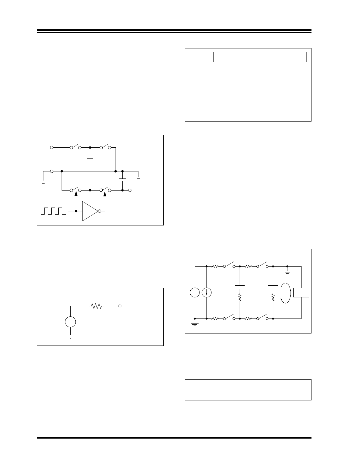
4.0
DETAILED DESCRIPTION
4.1
Theory of Operation
The TC7660 charge pump converter inverts the voltage
applied to the V
+
pin. The conversion consists of a two-
phase operation (
Figure 4-1
). During the first phase,
switches S
2
and S
4
are open and switches S
1
and S
3
are closed. C
1
charges to the voltage applied to the V
+
pin, with the load current being supplied from C
2
. Dur-
ing the second phase, switches S
2
and S
4
are closed
and switches S
1
and S
3
are open. Charge is trans-
ferred from C
1
to C
2
, with the load current being
supplied from C
1
.
FIGURE 4-1:
Ideal Switched Capacitor
Inverter.
In this manner, the TC7660 performs a voltage inver-
sion, but does not provide regulation. The average out-
put voltage will drop in a linear manner with respect to
load current. The equivalent circuit of the charge pump
inverter can be modeled as an ideal voltage source in
series with a resistor, as shown in
Figure 4-2
.
FIGURE 4-2:
Switched Capacitor Inverter
Equivalent Circuit Model.
The value of the series resistor (R
OUT
) is a function of
the switching frequency, capacitance and equivalent
series resistance (ESR) of C
1
and C
2
and the on-resis-
tance of switches S
1
, S
2
, S
3
and S
4
. A close
approximation for R
OUT
is given in the following
equation:
EQUATION
4.2
Switched Capacitor Inverter
Power Losses
The overall power loss of a switched capacitor inverter
is affected by four factors:
1.
Losses from power consumed by the internal
oscillator, switch drive, etc. These losses will
vary with input voltage, temperature and
oscillator frequency.
2.
Conduction losses in the non-ideal switches.
3.
Losses due to the non-ideal nature of the
external capacitors.
4.
Losses that occur during charge transfer from
C
1
to C
2
when a voltage difference between the
capacitors exists.
Figure 4-3
depicts the non-ideal elements associated
with the switched capacitor inverter power loss.
FIGURE 4-3:
Non-Ideal Switched
Capacitor Inverter.
The power loss is calculated using the following
equation:
EQUATION
V
+
GND S
3
S
1
S
2
S
4
C
2
V
OUT
= -V
IN
C
1
+
+
-
+
R
OUT
V
OUT
V
+
R
OUT
1
f
PUMP
C1
----------------------------- 8R
SW
4ESR
C1
ESR
C2
+
+
+
=
R
SW
on-resistance of the switches
=
ESR
C1
equivalent series resistance of C1
=
ESR
C2
equivalent series resistance of C2
=
f
PUMP
f
OSC
2
-----------
=
Where:
LOAD
C
1
C
2
R
SW
S
1
I
DD
ESR
C1
V
+
+
-
R
SW
S
2
R
SW
S
3
R
SW
S
4
ESR
C2
I
OUT
+
+
P
LOSS
I
OUT
2
R
OUT
I
DD
V
+
+
=
2002-2011 Microchip Technology Inc.
DS21465C-page 7
TC7660
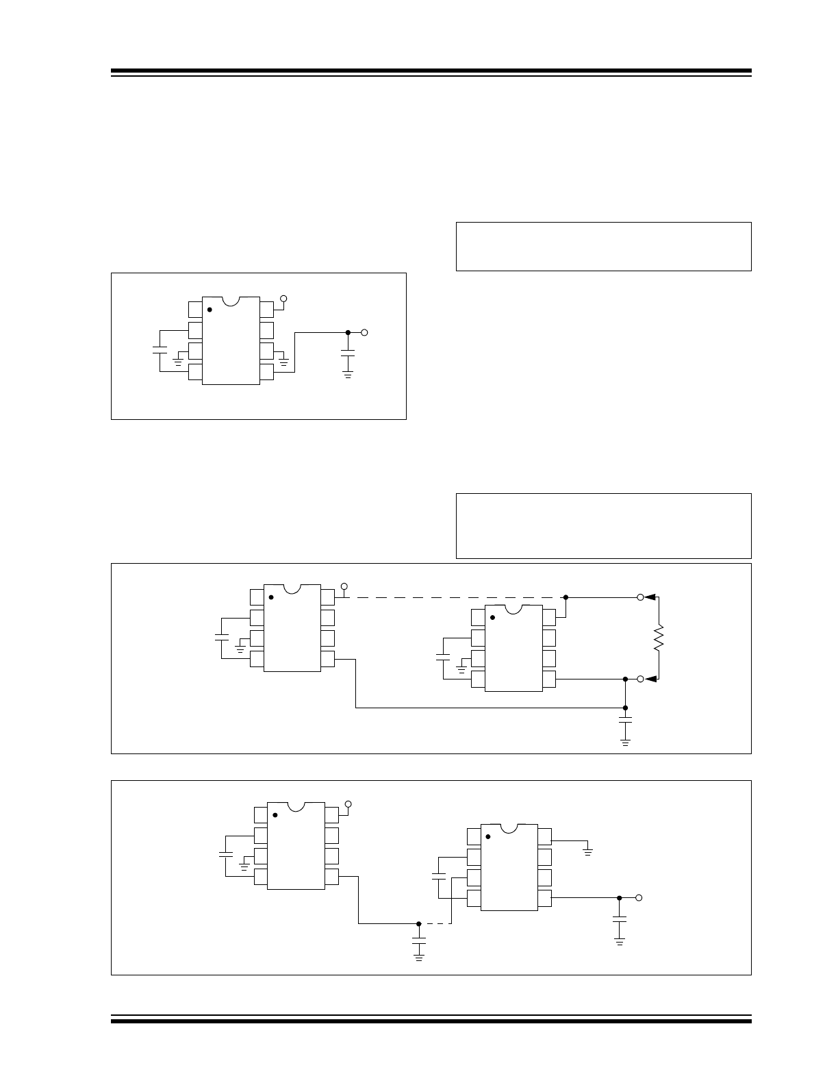
5.0
APPLICATIONS INFORMATION
5.1
Simple Negative Voltage
Converter
Figure 5-1
shows typical connections to provide a
negative supply where a positive supply is available. A
similar scheme may be employed for supply voltages
anywhere in the operating range of +1.5V to +10V,
keeping in mind that pin 6 (LV) is tied to the supply
negative (GND) only for supply voltages below 3.5V.
FIGURE 5-1:
Simple Negative Converter.
The output characteristics of the circuit in
Figure 5-1
are those of a nearly ideal voltage source in series with
a 70
resistor. Thus, for a load current of -10 mA and
a supply voltage of +5V, the output voltage would be
-4.3V.
5.2
Paralleling Devices
To reduce the value of R
OUT
, multiple TC7660 voltage
converters can be connected in parallel (
Figure 5-2
).
The output resistance will be reduced by approximately
a factor of n, where n is the number of devices
connected in parallel.
EQUATION
While each device requires its own pump capacitor
(C
1
), all devices may share one reservoir capacitor
(C
2
). To preserve ripple performance, the value of C
2
should be scaled according to the number of devices
connected in parallel.
5.3
Cascading Devices
A larger negative multiplication of the initial supply volt-
age can be obtained by cascading multiple TC7660
devices. The output voltage and the output resistance
will both increase by approximately a factor of n, where
n is the number of devices cascaded.
EQUATION
FIGURE 5-2:
Paralleling Devices Lowers Output Impedance.
FIGURE 5-3:
Increased Output Voltage By Cascading Devices.
+
V
+
+
1
2
3
4
8
7
6
5
TC7660
V
OUT
*
C
1
10 µF
* V
OUT
= -V
+
for 1.5V
V+ 10V
C
2
10 µF
R
OUT
R
OUT
of TC7660
n number of devices
---------------------------------------------------------
=
V
OUT
n
–
V
+
=
R
OUT
n R
OUT
of TC7660
=
“n”
“1”
R
L
+
V
+
+
1
2
3
4
8
7
6
5
TC7660
C
1
C
2
+
1
2
3
4
8
7
6
5
TC7660
C
1
V
OUT
*
“1”
+
V
+
+
1
2
3
4
8
7
6
5
TC7660
10 µF
* V
OUT
= -n V
+
for 1.5V
V+ 10V
“n”
+
1
2
3
4
8
7
6
5
TC7660
10 µF
10 µF
+
10 µF
TC7660
DS21465C-page 8
2002-2011 Microchip Technology Inc.
5.4
Changing the TC7660 Oscillator
Frequency
The operating frequency of the TC7660 can be
changed in order to optimize the system performance.
The frequency can be increased by over-driving the
OSC input (
Figure 5-4
). Any CMOS logic gate can be
utilized in conjunction with a 1 k
series resistor. The
resistor is required to prevent device latch-up. While
TTL level signals can be utilized, an additional 10 k
pull-up resistor to V
+
is required. Transitions occur on
the rising edge of the clock input. The resultant output
voltage ripple frequency is one half the clock input.
Higher clock frequencies allow for the use of smaller
pump and reservoir capacitors for a given output volt-
age ripple and droop. Additionally, this allows the
TC7660 to be synchronized to an external clock,
eliminating undesirable beat frequencies.
At light loads, lowering the oscillator frequency can
increase the efficiency of the TC7660 (
Figure 5-5
). By
lowering the oscillator frequency, the switching losses
are reduced. Refer to
Figure 2-3
to determine the typi-
cal operating frequency based on the value of the
external capacitor. At lower operating frequencies, it
may be necessary to increase the values of the pump
and reservoir capacitors in order to maintain the
desired output voltage ripple and output impedance.
FIGURE 5-4:
External Clocking.
FIGURE 5-5:
Lowering Oscillator
Frequency.
5.5
Positive Voltage Multiplication
Positive voltage multiplication can be obtained by
employing two external diodes (
Figure 5-6
). Refer to
the theory of operation of the TC7660 (
Section 4.1
“Theory of Operation”
). During the half cycle when
switch S
2
is closed, capacitor C
1
of
Figure 5-6
is
charged up to a voltage of V
+
- V
F1
, where V
F1
is the
forward voltage drop of diode D
1
. During the next half
cycle, switch S
1
is closed, shifting the reference of
capacitor C
1
from GND to V
+
. The energy in capacitor
C
1
is transferred to capacitor C
2
through diode D
2
, pro-
ducing an output voltage of approximately:
EQUATION
FIGURE 5-6:
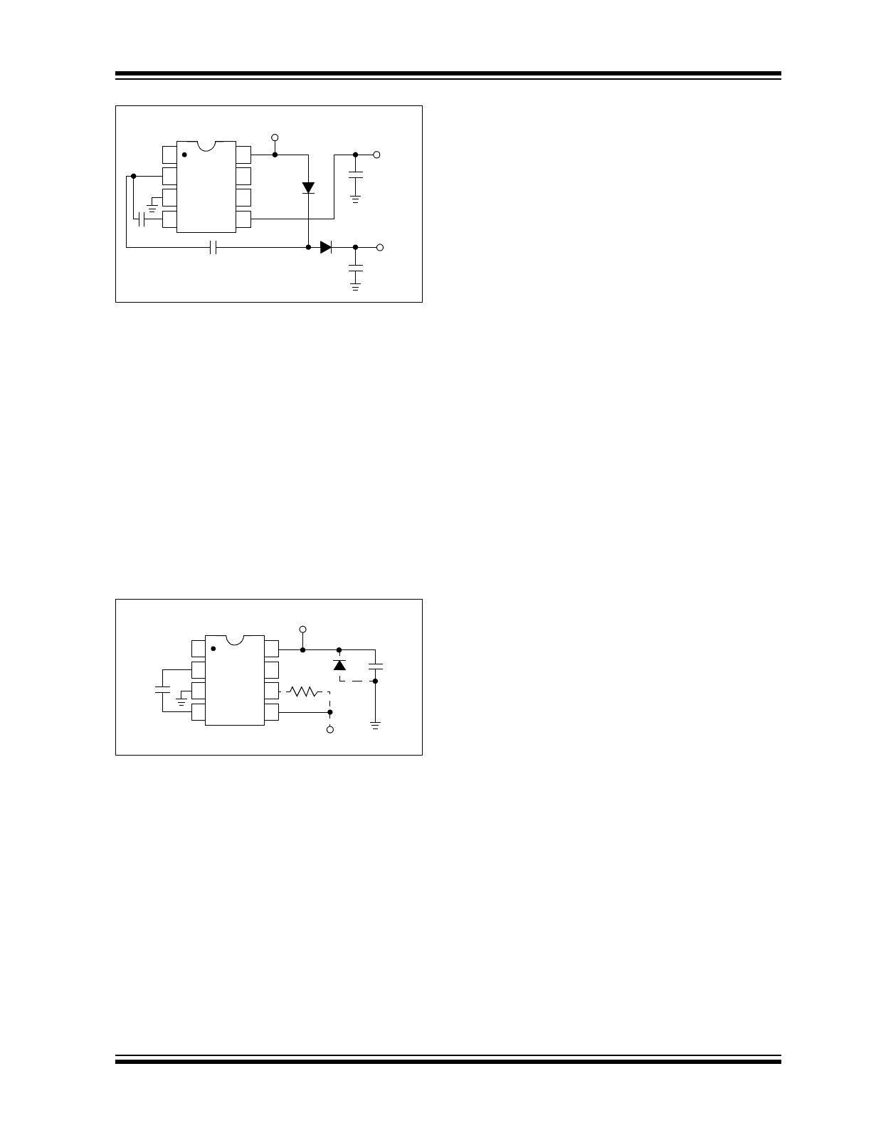
Positive Voltage Multiplier.
5.6
Combined Negative Voltage
Conversion and Positive Supply
Multiplication
Simultaneous voltage inversion and positive voltage
multiplication can be obtained (
Figure 5-7
). Capacitors
C
1
and C
3
perform the voltage inversion, while capaci-
tors C
2
and C
4
, plus the two diodes, perform the posi-
tive voltage multiplication. Capacitors C
1
and C
2
are
the pump capacitors, while capacitors C
3
and C
4
are
the reservoir capacitors for their respective functions.
Both functions utilize the same switches of the TC7660.
As a result, if either output is loaded, both outputs will
drop towards GND.
CMOS
GATE
1 k
V
OUT
“1”
+
V
+
+
1
2
3
4
8
7
6
5
TC7660
10 µF
10 µF
V
+
V
OUT
+
+
1
2
3
4
8
7
6
5
TC7660
C
1
C
2
V
+
C
OSC
V
OUT
2 V
+
V
F1
V
F2
+
–
=
where:
V
F1
is the forward voltage drop of diode D
1
and
V
F2
is the forward voltage drop of diode D
2
.
+
C
2
D
1
D
2
+
C
1
V
OUT
=
1
2
3
4
8
7
6
5
TC7660
V
+
(2 V
+
) - (2 V
F
)
2002-2011 Microchip Technology Inc.
DS21465C-page 9
TC7660
FIGURE 5-7:
Combined Negative
Converter
and Positive Multiplier.
5.7
Efficient Positive Voltage
Multiplication/Conversion
Since the switches that allow the charge pumping
operation are bidirectional, the charge transfer can be
performed backwards as easily as forwards.
Figure 5-8
shows a TC7660 transforming -5V to +5V
(or +5V to +10V, etc.). The only problem here is that the
internal clock and switch-drive section will not operate
until some positive voltage has been generated. An ini-
tial inefficient pump, as shown in
Figure 5-7
, could be
used to start this circuit up, after which it will bypass the
other (D
1
and D
2
in
Figure 5-7
would never turn on), or
else the diode and resistor shown dotted in
Figure 5-8
can be used to “force” the internal regulator on.
FIGURE 5-8:
Positive Voltage
Conversion.
+
C
1
D
1
+
+
C
3
C
4
C
2
D
2
+
V
OUT
=
1
2
3
4
8
7
6
5
TC7660
V
+
(2 V
+
) - (2 V
F
)
V
OUT
= -V
+
V
OUT
= -V
-
+
1 M
V
-
input
+
1
2
3
4
8
7
6
5
TC7660
10 µF
10 µF
C
1
TC7660
DS21465C-page 10
2002-2011 Microchip Technology Inc.
6.0
PACKAGING INFORMATION
6.1
Package Marking Information
Note:
In the event the full Microchip part number cannot be marked on one line, it will
be carried over to the next line thus limiting the number of available characters
for customer specific information.
Legend: XX...X
Customer-specific information
Y
Year code (last digit of calendar year)
YY
Year code (last 2 digits of calendar year)
WW
Week code (week of January 1 is week ‘01’)
NNN
Alphanumeric traceability code
Pb-free JEDEC designator for Matte Tin (Sn)
*
This package is Pb-free. The Pb-free JEDEC designator ( )
can be found on the outer packaging for this package.
3
e
3
e
TC7660C
OA 1208
3
e
8-Lead SOIC (3.90 mm)
Example
NNN
Example
TC7660C
OA1208
256
256
8-Lead CERDIP (.300”)
Example
XXXXXNNN
XXXXXXXX
YYWW
Example
TC7660
MJA 256
TC7660
MJA256
3
e
1208
1208
8-Lead PDIP (300 mil)
Example
XXXXXXXX
XXXXXNNN
YYWW
Example
TC7660
CPA 256
3
e
TC7660
CPA256
1208
1208