
2017 Microchip Technology Inc.
DS20005697A-page 1
TC6320
Features
• Integrated Gate-to-source Resistor
• Integrated Gate-to-source Zener Diode
• Low Threshold
• Low On-resistance
• Low Input Capacitance
• Fast Switching Speeds
• Free from Secondary Breakdown
• Low Input and Output Leakage
• Independent Electrically Isolated N-channel and
P-channel
Applications
• High-voltage Pulsers
• Amplifiers
• Buffers
• Piezoelectric Transducer Drivers
• General Purpose Line Drivers
• Logic-level Interfaces
General Description
The TC6320 consists of high-voltage, low-threshold
N-channel and P-channel MOSFETs in 8-lead SOIC
and DFN packages. Both MOSFETs have integrated
gate-to-source resistors and gate-to-source Zener
diode clamps which are desired for high-voltage pulser
applications. It is a complimentary, high-speed,
high-voltage, gate-clamped N-channel and P-channel
MOSFET pair, which utilizes an advanced vertical
DMOS structure and a well-proven silicon gate
manufacturing process. This combination produces a
device with the power handling capabilities of bipolar
transistors and with the high input impedance and
positive temperature coefficient inherent in MOS
devices. Characteristic of all MOS structures, this
device is free from thermal runaway and thermally
induced secondary breakdown.
Microchip’s vertical DMOS FETs are ideally suited to a
wide range of switching and amplifying applications
where very low threshold voltage, high breakdown
voltage, high input impedance, low input capacitance
and fast switching speeds are desired.
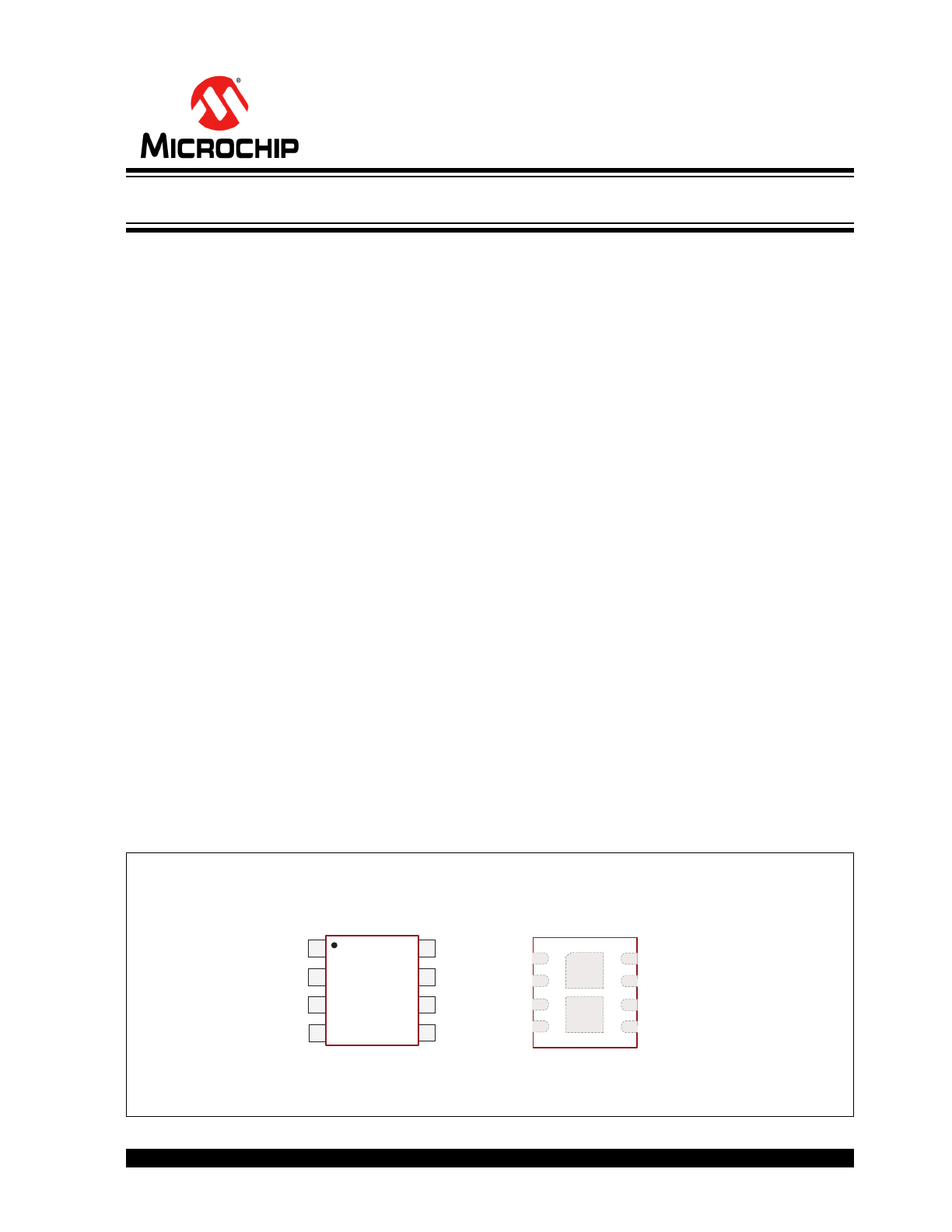
Package Type
8-lead SOIC
(Top view)
See
Table 2-1
and
Table 2-2
for pin information.
8
7
6
5
1
2
3
4
SN
GN
SP
GP
DN
DN
DP
DP
5-lead DFN
(Top view)
8
7
6
5
1
2
3
4
SN
GN
GP
SP
DN
DN
DP
DP
DN
DP
s
N-Channel and P-Channel Enhancement-Mode MOSFET Pair
TC6320
DS20005697A-page 2
2017 Microchip Technology Inc.
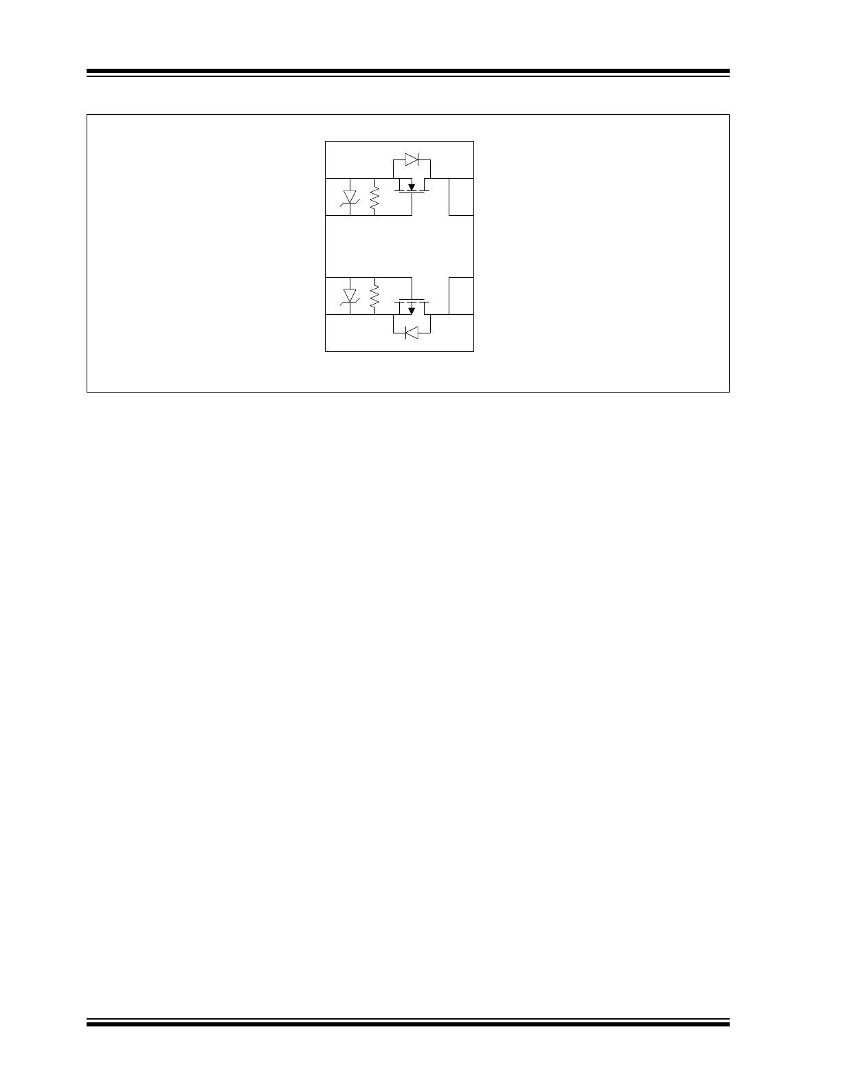
Functional Block Diagram
N-Channel
P-Channel
DN
DN
DP
DP
SN
GN
GP
SP
2017 Microchip Technology Inc.
DS20005697A-page 3
TC6320
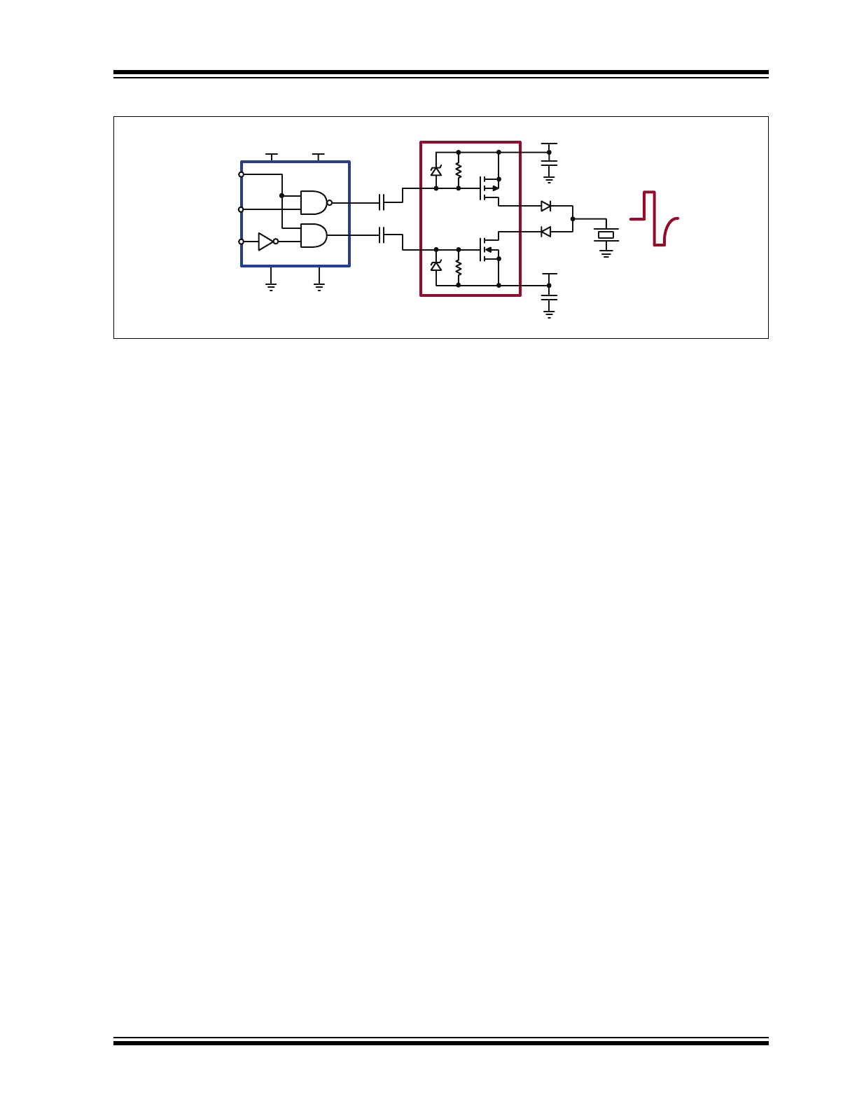
Typical Application Circuit
VSS
VL
VDD
VH
INA
INB
OE
-100V
+100V
TC6320
10nF
10nF
MD12xx, MD17xx, or MD18xx
TC6320
DS20005697A-page 4
2017 Microchip Technology Inc.
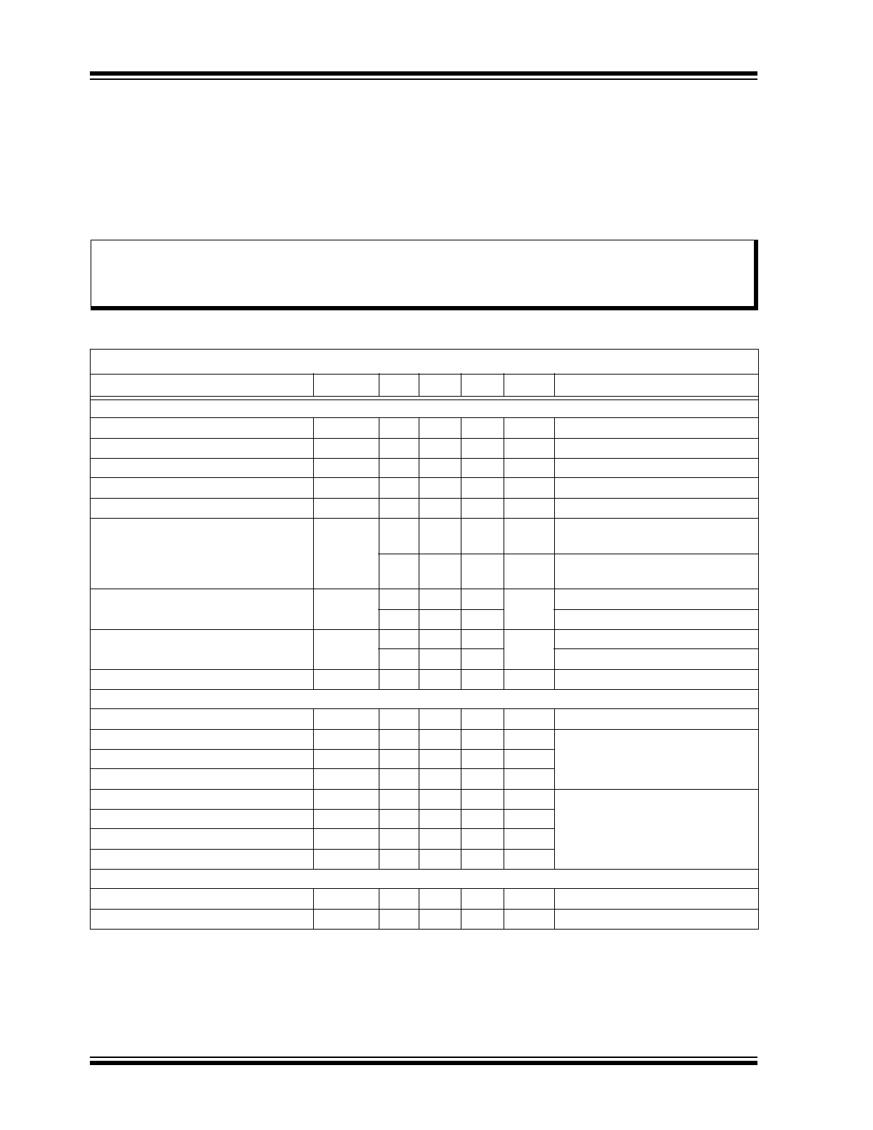
1.0
ELECTRICAL CHARACTERISTICS
Absolute Maximum Ratings†
Drain-to-source Voltage ........................................................................................................................................ BV
DSS
Drain-to-gate Voltage ........................................................................................................................................... BV
DGS
Operating Ambient Temperature, T
A
................................................................................................... –55°C to +150°C
Storage Temperature, T
S
..................................................................................................................... –55°C to +150°C
† Notice: Stresses above those listed under “Absolute Maximum Ratings” may cause permanent damage to the
device. This is a stress rating only, and functional operation of the device at those or any other conditions above those
indicated in the operational sections of this specification is not intended. Exposure to maximum rating conditions for
extended periods may affect device reliability.
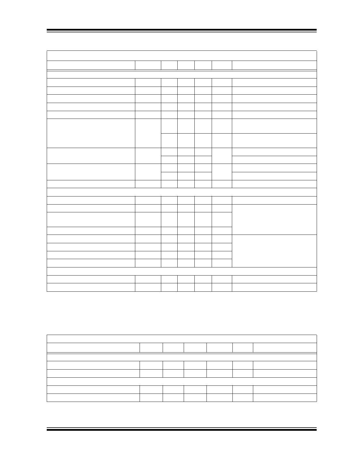
N-CHANNEL ELECTRICAL CHARACTERISTICS
Electrical Specifications: T
A
= T
J
= 25°C unless otherwise specified.
Parameter
Sym.
Min.
Typ.
Max.
Unit
Conditions
DC PARAMETER (
Note 1
unless otherwise specified)
Drain-to-source Breakdown Voltage
BV
DSS
200
—
—
V
V
GS
= 0V, I
D
= 2 mA
Gate Threshold Voltage
V
GS(th)
1
—
2
V
V
GS
= V
DS
, I
D
= 1 mA
Change in V
GS(th)
with Temperature
∆V
GS(th)
—
—
–4.5
mV/°C V
GS
= V
DS
, I
D
= 1 mA (
Note 2
)
Gate-to-source Shunt Resistor
R
GS
10
—
50
kΩ
I
GS
= 100 µA
Gate-to-Source Zener Voltage
VZ
GS
13.2
—
25
V
I
GS
= 2 mA
Zero-gate Voltage Drain Current
I
DSS
—
—
10
µA
V
DS
= Maximum rating,
V
GS
= 0V
—
—
1
mA
V
DS
= 0.8 Maximum rating,
V
GS
= 0V, T
A
= 125°C (
Note 2
)
On-state Drain Current
I
D(ON)
1
—
—
A
V
GS
= 4.5V, V
DS
= 25V
2
—
—
V
GS
= 10V, V
DS
= 25V
Static Drain-to-source On-state
Resistance
R
DS(ON)
—
—
8
Ω
V
GS
= 4.5V, I
D
= 150 mA
—
—
7
V
GS
= 10V, I
D
= 1A
Change in R
DS(ON)
with Temperature
∆R
DS(ON)
—
—
1
%/°C
V
GS
= 4.5V, I
D
= 150 mA (
Note 2
)
AC PARAMETER (
Note 2
)
Forward Transconductance
G
FS
400
—
—
mmho V
DS
= 25V, I
D
= 500 mA
Input Capacitance
C
ISS
—
—
110
pF
V
GS
= 0V,
V
DS
= 25V,
f = 1 MHz
Common Source Output Capacitance
C
OSS
—
—
60
pF
Reverse Transfer Capacitance
C
RSS
—
—
23
pF
Turn-on Delay Time
t
d(ON)
—
—
10
ns
V
DD
= 25V,
I
D
= 1A,
R
GEN
= 25Ω
Rise Time
t
r
—
—
15
ns
Turn-off Delay Time
t
d(OFF)
—
—
20
ns
Fall Time
t
f
—
—
15
ns
DIODE PARAMETER
Diode Forward Voltage Drop
V
SD
—
—
1.8
V
V
GS
= 0V, I
SD
= 500 mA (
Note 1
)
Reverse Recovery Time
t
rr
—
300
—
ns
V
GS
= 0V, I
SD
= 500 mA (
Note 2
)
Note 1: All DC parameters are 100% tested at 25°C unless otherwise stated. Pulse test: 300 µs pulse, 2% duty
cycle.
2: Specification is obtained by characterization and is not 100% tested.
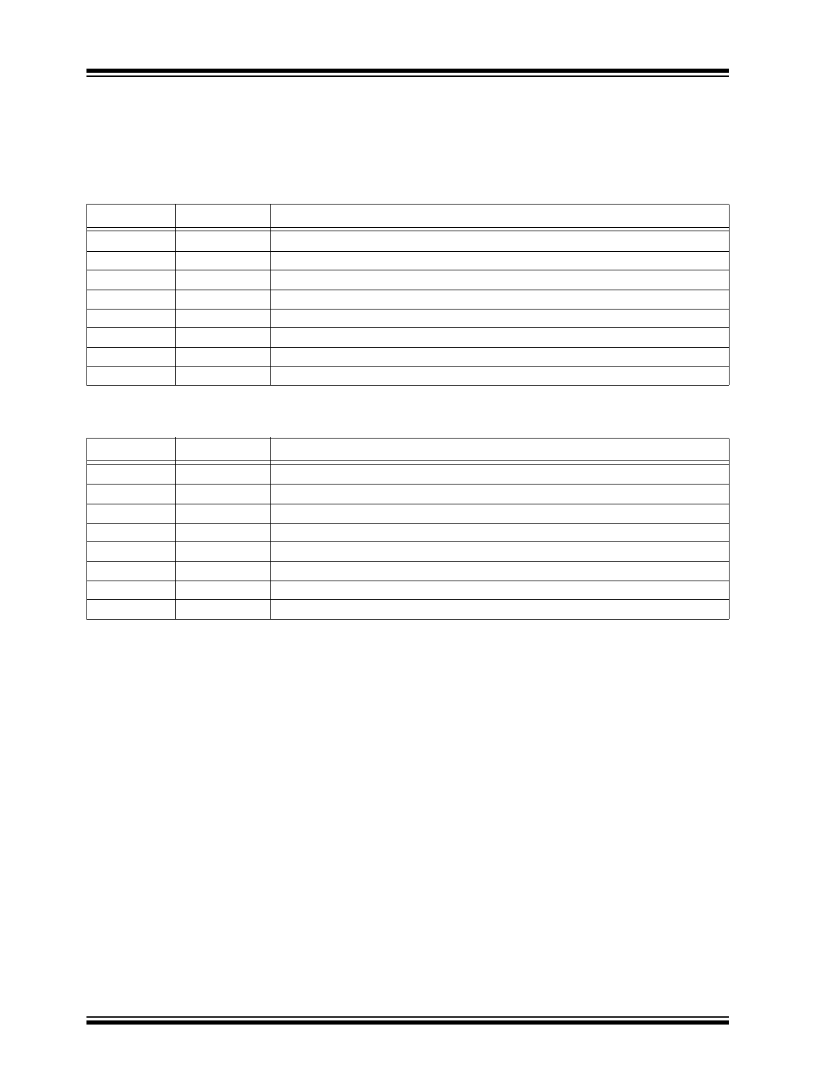
P-CHANNEL ELECTRICAL CHARACTERISTICS
Electrical Specifications: T
A
= T
J
= 25°C unless otherwise specified.
Parameter
Sym.
Min.
Typ.
Max.
Unit
Conditions
DC PARAMETER (
Note 1
unless otherwise specified)
Drain-to-source Breakdown Voltage
BV
DSS
–200
—
—
V
V
GS
= 0V, I
D
= –2 mA
Gate Threshold Voltage
V
GS(th)
–1
—
–2.4
V
V
GS
= V
DS
, I
D
= –1 mA
Change in V
GS(th)
with Temperature
∆V
GS(th)
—
—
4.5
mV/°C V
GS
= V
DS
, I
D
= –1 mA (
Note 2
)
Gate-to-source Shunt Resistor
R
GS
10
—
50
kΩ
I
GS
= 100 µA
Gate-to-Source Zener Voltage
VZ
GS
13.2
—
25
V
I
GS
= –2 mA
Zero-gate Voltage Drain Current
I
DSS
—
—
–10
µA
V
DS
= Maximum rating,
V
GS
= 0V
—
—
–1
mA
V
DS
= 0.8 Maximum rating,
V
GS
= 0V, T
A
= 125°C (
Note 2
)
On-state Drain Current
I
D(ON)
–1
—
—
A
V
GS
= –4.5V, V
DS
= –25V
–2
—
—
V
GS
= –10V, V
DS
= –25V
Static Drain-to-source On-state
Resistance
R
DS(ON)
—
—
10
Ω
V
GS
= –4.5V, I
D
= –150 mA
—
—
8
V
GS
= –10V, I
D
= –1A
Change in R
DS(ON)
with Temperature ∆R
DS(ON)
—
—
1
%/°C
V
GS
= –10V, I
D
= –200 mA (
Note 2
)
AC PARAMETER (
Note 2
)
Forward Transconductance
G
FS
400
—
—
mmho V
DS
= –25V, I
D
= –500 mA
Input Capacitance
C
ISS
—
—
200
pF
V
GS
= 0V,
V
DS
= –25V,
f = 1 MHz
Common Source Output
Capacitance
C
OSS
—
—
55
pF
Reverse Transfer Capacitance
C
RSS
—
—
30
pF
Turn-on Delay Time
t
d(ON)
—
—
10
ns
V
DD
= –25V,
I
D
= –1A,
R
GEN
= 25Ω
Rise Time
t
r
—
—
15
ns
Turn-off Delay Time
t
d(OFF)
—
—
20
ns
Fall Time
t
f
—
—
15
ns
DIODE PARAMETER
Diode Forward Voltage Drop
V
SD
—
—
–1.8
V
V
GS
= 0V, I
SD
= –500 mA (
Note 1
)
Reverse Recovery Time
t
rr
—
300
—
ns
V
GS
= 0V, I
SD
= –500 mA (
Note 2
)
Note 1: All DC parameters are 100% tested at 25°C unless otherwise stated. Pulse test: 300 µs pulse, 2% duty
cycle.
2: Specification is obtained by characterization and is not 100% tested.
TEMPERATURE SPECIFICATIONS
Electrical Characteristics: Unless otherwise specified, for all specifications T
A
=T
J
= +25°C.
Parameter
Sym.
Min.
Typ.
Max.
Unit
Conditions
TEMPERATURE RANGE
Operating Ambient Temperature
T
A
–55°C
—
+150
°C
Storage Temperature
T
S
–55°C
—
+150
°C
PACKAGE THERMAL RESISTANCE
8-lead DFN
JA
—
44
—
°C/W
Note 1
8-lead SOIC
JA
—
101
—
°C/W
Note 1
2017 Microchip Technology Inc.
DS20005697A-page 5
TC6320
Note 1: 1 oz., four-layer, 3” x 4” PCB
TC6320
DS20005697A-page 6
2017 Microchip Technology Inc.
2.0
PIN DESCRIPTION
Table 2-1
and
Table 2-2
show the description of pins in
TC6320 8-lead DFN and 8-lead SOIC, respectively.
Refer to
Package Types
for the location of pins.
TABLE 2-1:
8-LEAD DFN PIN FUNCTION TABLE
Pin Number
Pin Name
Description
1
SN
Source N-channel
2
GN
Gate N-channel
3
GP
Gate P-channel
4
SP
Source P-channel
5
DP
Drain P-channel
6
DP
Drain P-channel
7
DN
Drain N-channel
8
DN
Drain N-channel
TABLE 2-2:
8-LEAD SOIC FUNCTION TABLE
Pin Number
Pin Name
Description
1
SN
Source N-channel
2
GN
Gate N-channel
3
SP
Source P-channel
4
GP
Gate P-channel
5
DP
Drain P-channel
6
DP
Drain P-channel
7
DN
Drain N-channel
8
DN
Drain N-channel
2017 Microchip Technology Inc.
DS20005697A-page 7
TC6320
3.0
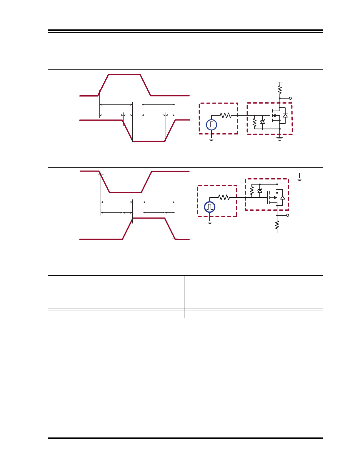
FUNCTIONAL DESCRIPTION
Figure 3-1
and
Figure 3-2
illustrate the switching
waveforms and test circuits for TC6320.
10V
0V
0V
VDD
Input
Output
10%
90%
90%
10%
90%
10%
R
GEN
Input
Pulse
Generator
V
DD
R
L
D.U.T
OUTPUT
t
r
t
f
t
d(ON)
t
(ON)
t
d(OFF)
t
(OFF)
FIGURE 3-1:
N-Channel Switching Waveforms and Test Circuit.
R
GEN
Input
Pulse
Generator
V
DD
R
L
D.U.T
OUTPUT
0V
-10V
0V
VDD
Input
Output
t
r
t
f
t
d(ON)
t
(ON)
90%
10%
90%
10%
10%
90%
t
d(OFF)
t
(OFF)
FIGURE 3-2:
P-Channel Switching Waveforms and Test Circuit.
PRODUCT SUMMARY
BV
DSS
/BV
DGS
(V)
R
DS(ON)
(Maximum)
(Ω)
N-Channel
P-Channel
N-Channel
P-Channel
200
–200
7
8
TC6320
DS20005697A-page 8
2017 Microchip Technology Inc.
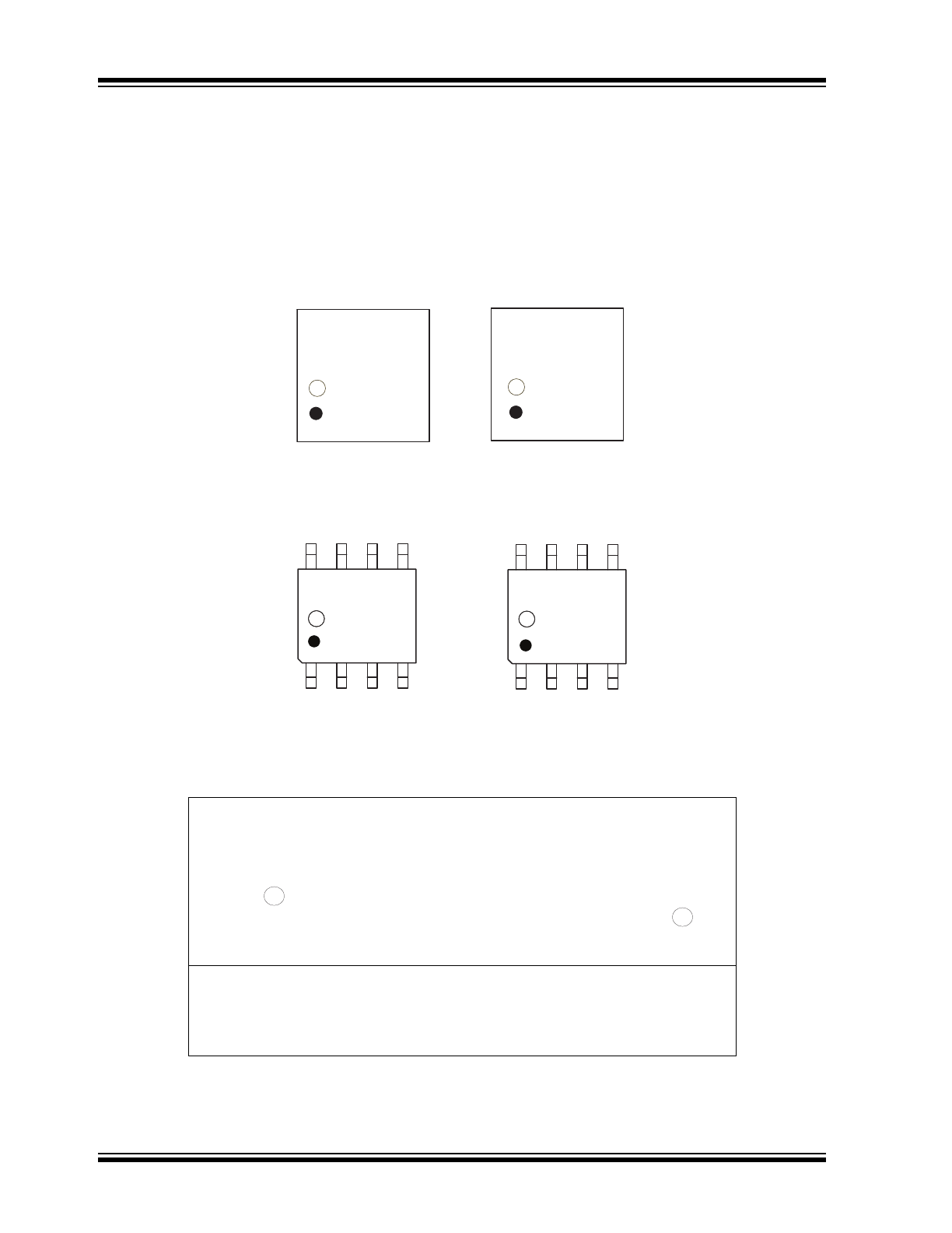
4.0
PACKAGING INFORMATION
4.1
Package Marking Information
Legend: XX...X
Product Code or Customer-specific information
Y
Year code (last digit of calendar year)
YY
Year code (last 2 digits of calendar year)
WW
Week code (week of January 1 is week ‘01’)
NNN
Alphanumeric traceability code
Pb-free
JEDEC
®
designator for Matte Tin (Sn)
*
This package is Pb-free. The Pb-free JEDEC designator ( )
can be found on the outer packaging for this package.
Note:
In the event the full Microchip part number cannot be marked on one line, it will
be carried over to the next line, thus limiting the number of available
characters for product code or customer-specific information. Package may or
not include the corporate logo.
3
e
3
e
8-lead DFN
Example
NNN
XXXXXXX
XXXXXXX
YYWW
e3
222
K6
TC6320
1715
e3
8-lead SOIC
Example
NNN
XXXXXXX
YYWW
555
TC6320TG
1727
e3
e3
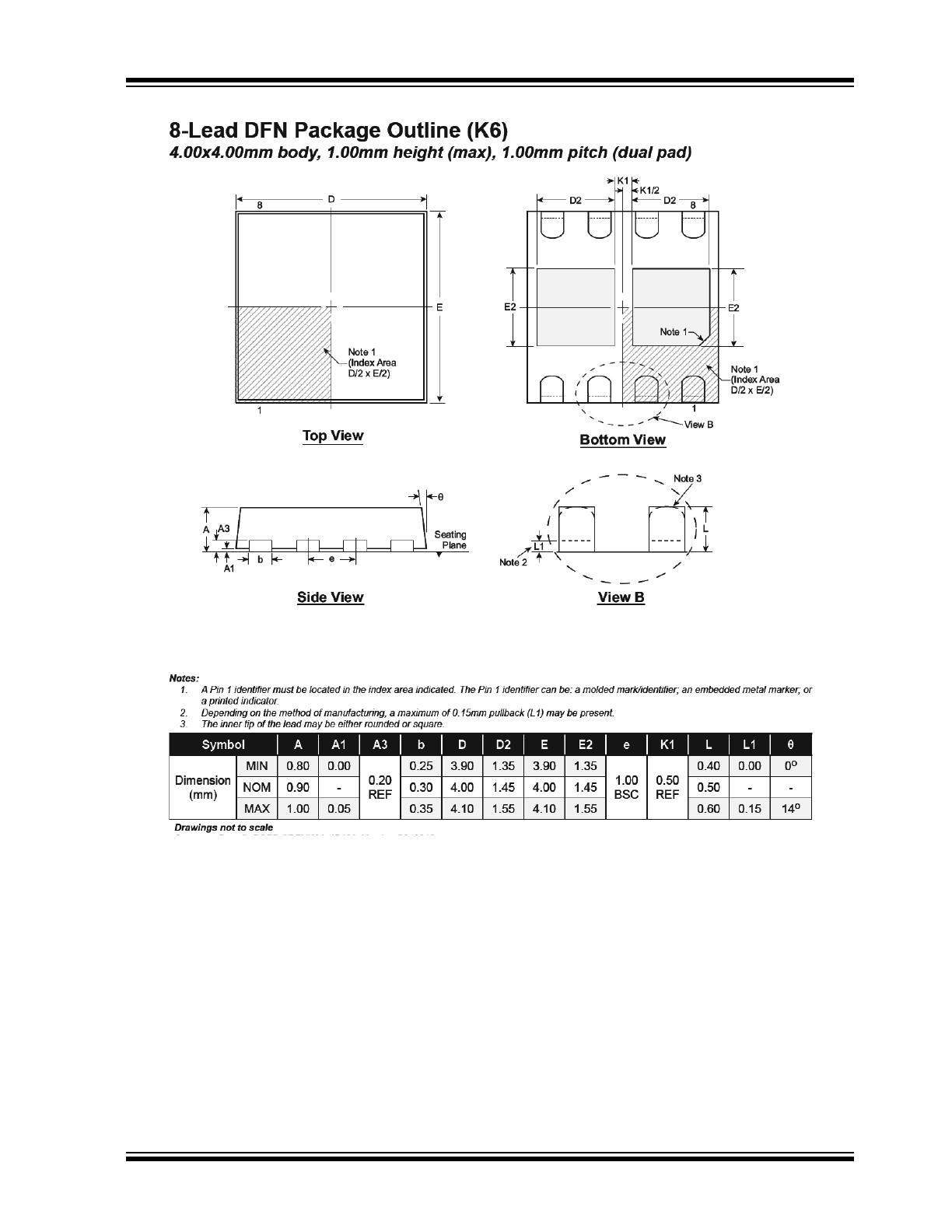
Note: For the most current package drawings, see the Microchip Packaging Specification at www.microchip.com/packaging.
2017 Microchip Technology Inc.
DS20005697A-page 9
TC6320
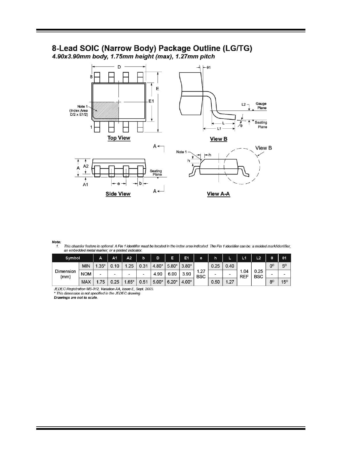
Note: For the most current package drawings, see the Microchip Packaging Specification at www.microchip.com/packaging.
TC6320
DS20005697A-page 10
2017 Microchip Technology Inc.