
2001-2014 Microchip Technology Inc.
DS20001434K-page 1
TC54
Features:
• ±2.0% Detection Thresholds
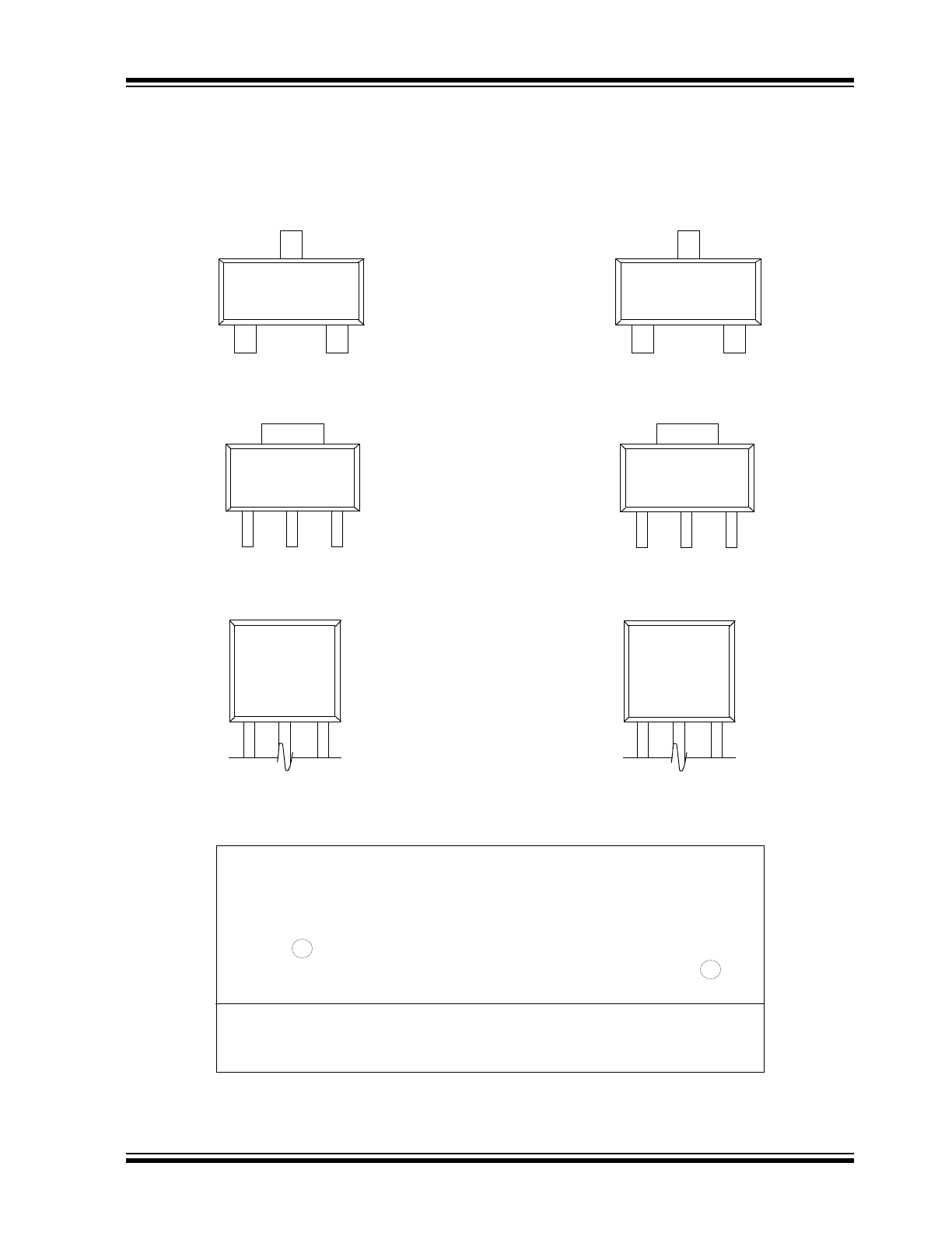
• Small Packages: 3-Pin SOT-23A, SOT-89, and
TO-92
• Low Current Drain: 1 µA, typical
• Wide Detection Range: 1.1V to 6.0V
• Wide Operating Voltage Range: 0.7V to 10V
Applications:
• Battery Voltage Monitoring
• Microprocessor Reset
• System Brown-Out Protection
• Switching Circuit in Battery Backup
• Level Discriminator
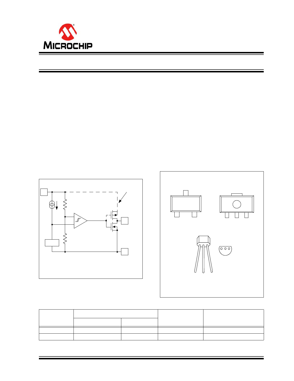
Functional Block Diagram
General Description:
The TC54 series are CMOS voltage detectors espe-
cially well-suited for battery-powered applications
because of their extremely low 1 µA operating current
and small surface-mount packaging. Each part is laser-
trimmed to the desired threshold voltage, which can be
specified from 1.4V to 6.0V with a 2% tolerance.
The TC54 is available with either an open-drain or com-
plementary output stage. During operation, the output
(V
OUT
) remains in the logic-high state as long as V
IN
is
greater than the specified threshold voltage (V
DET
–).
When V
IN
falls below V
DET
–, the output is driven to a
logic-low. V
OUT
remains low until V
IN
rises above
V
DET
– by an amount V
HYST
, when it resets to a logic-
high state.
Package Types
Device Features
V
OUT
V
SS
+
–
V
IN
V
REF
TC54VC only
TC54VN has open-drain output.
TC54VC has complementary (push-pull) output.
1
3
2
V
IN
V
SS
V
OUT
TC54
3-Pin SOT-89
Note:
3-Pin SOT-23A is equivalent to the
EIAJ SC-59.
3-Pin TO-92
1 2 3
V
SS
V
IN
V
OUT
V
IN
V
OUT
V
SS
3
1
2
TC54
3-Pin SOT-23A
V
IN
Device
Output
Reset Delay
Std. Trip Points
(
1
)
(typical)
Type
State
TC54VN
Open-Drain
Active Low
No
1.4V, 2.1V, 2.7V, 2.9V
TC54VC
Push-Pull
Active Low
No
3.0V, 4.2V, 4.3V
Note 1:
Custom Trip Points available. Minimum order requirement. Information available upon request.
Voltage Detector
TC54
DS20001434K-page 2
2001-2014 Microchip Technology Inc.
1.0
ELECTRICAL
CHARACTERISTICS
Absolute Maximum Ratings †
Input Voltage ...................................................................+12V
Output Current ..............................................................50 mA
Output Voltage: CMOS................(V
SS
– 0.3V) to (V
IN
+ 0.3V)
Open-Drain.....................(V
SS
– 0.3V) to 12V
Power Dissipation (T
A
70°C):
3-Pin SOT-23A .......................................................240 mW
3-Pin SOT-89..........................................................500 mW
3-Pin TO-92 ............................................................300 mW
Operating Temperature Range........................-40°C to +85°C
Storage Temperature Range .........................-65°C to +150°C
† Notice: Stresses above those listed under "Absolute Maxi-
mum Ratings" may cause permanent damage to the device.
These are stress ratings only and functional operation of the
device at these or any other conditions above those indicated
in the operation sections of the specifications is not implied.
Exposure to Absolute Maximum Rating conditions for
extended periods may affect device reliability.
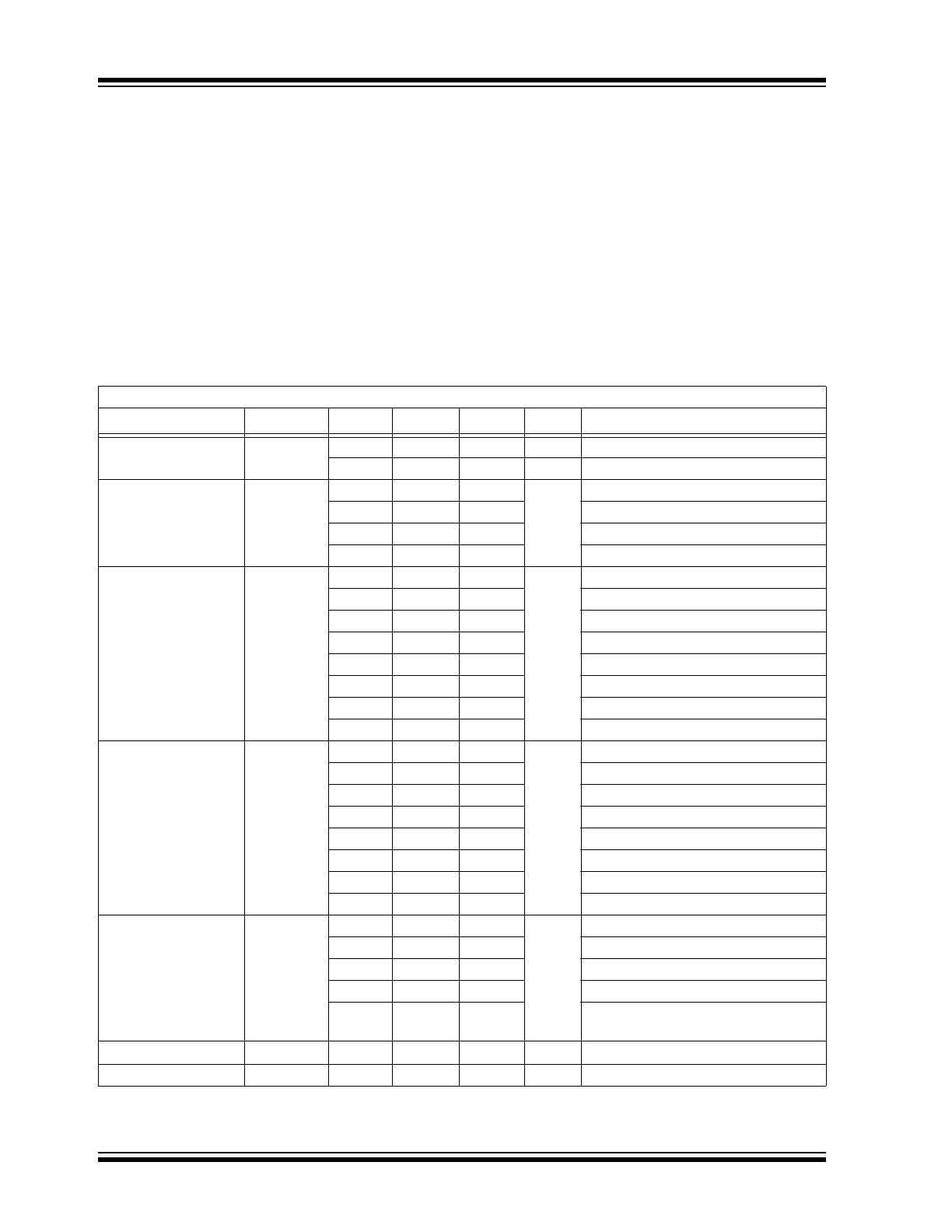
DC CHARACTERISTICS
Electrical Specifications: Unless otherwise noted, T
A
= +25°C.
Parameter
Symbol
Min.
Typ.
Max.
Units
Test Conditions
Operating Voltage
V
IN
0.7
—
10.0
V
(V
DET
–)
1.6V
0.7
—
6.0
V
(V
DET
–) < 1.6V
Quiescent Current
I
SS
—
0.8
2.7
µA
V
IN
= 2.0V
—
0.9
3.0
V
IN
= 3.0V
—
1.0
3.2
V
IN
= 4.0V
—
1.1
3.6
V
IN
= 5.0V
Threshold Voltage
(
Note 1
)
V
DET
–
1.37
1.4
1.43
V
TC54VX14
2.06
2.1
2.14
TC54VX21
2.65
2.7
2.75
TC54VX27
2.84
2.9
2.96
TC54VX29
2.94
3.0
3.06
TC54VX30
4.12
4.2
4.28
TC54VX42
4.21
4.3
4.39
TC54VX43
N.M-2%
N.M
N.M+2%
TC54VXNM (
Note 2
)
Hysteresis Voltage
V
HYST
28
70
112
mV
V
DET
= 1.4V (typical)
42
105
168
V
DET
= 2.1V (typical)
54
135
216
V
DET
= 2.7V (typical)
58
145
232
V
DET
= 2.9V (typical)
60
150
240
V
DET
= 3.0V (typical)
84
210
336
V
DET
= 4.2V (typical)
86
215
344
V
DET
= 4.3V (typical)
Q-60%
Q
Q+60%
V
DET
= (20*Q)V (typical) (
Note 2
)
Output Current
I
OUT
3.0
7.7
—
mA
V
OL
= 0.5V, V
IN
= 2.0V
5.0
10.1
—
V
OL
= 0.5V, V
IN
= 3.0V
6.0
11.5
—
V
OL
= 0.5V, V
IN
= 4.0V
7.0
13.0
—
V
OL
= 0.5V, V
IN
= 5.0V
—
-10.0
-2.0
TC54VC Only:
V
OH
= V
IN
– 2.1V, V
IN
= 8.0V
Tempco of (V
DET
–)
T
C
(V
DET
–)
—
±100
—
ppm/°C -40°C
T
A
85°C
Delay Time
t
DLY
—
—
0.2
ms
V
DET
–
V
OUT
inversion
Note 1:
For other voltage options, please contact your regional Microchip sales office.
2:
Represents all other custom Threshold Voltage options.
2001-2014 Microchip Technology Inc.
DS20001434K-page 3
TC54
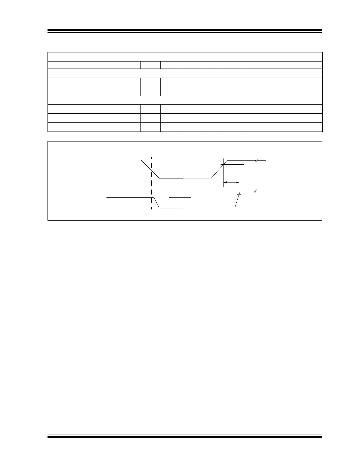
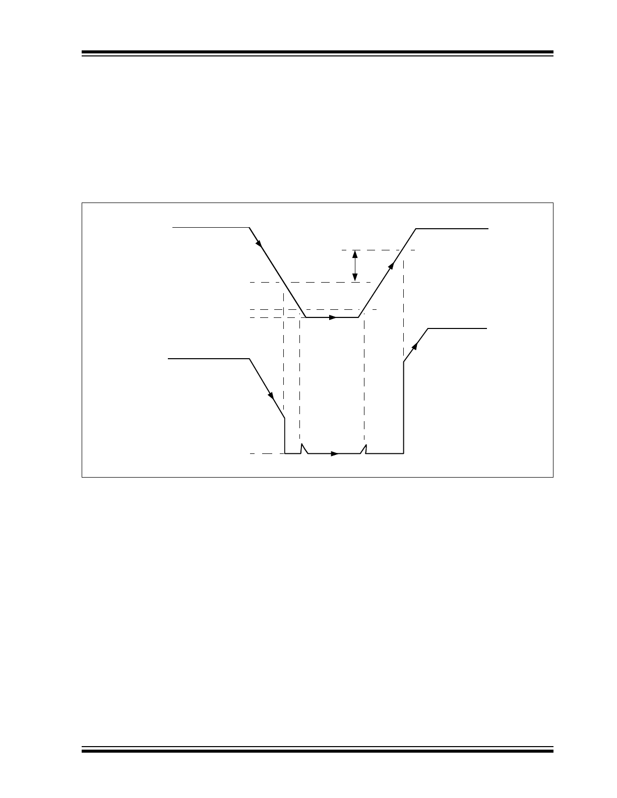
FIGURE 1-1:
Timing Diagram.
TEMPERATURE SPECIFICATIONS
Electrical Characteristics: Unless otherwise indicated, all limits are specified for: V
DD
=+1.8V to +5.5V, V
SS
= GND.
Parameters
Sym.
Min.
Typ.
Max.
Units
Conditions
Temperature Ranges
Operating Temperature Range
T
A
-40
—
+85
°C
Storage Temperature Range
T
A
-65
—
+150
°C
Thermal Package Resistances
Thermal Resistance, 3L-SOT-23A
JA
—
308
—
°C/W
Thermal Resistance, 3L-SOT-89
JA
—
131.7
—
°C/W
Thermal Resistance, 3L-TO-92
JA
—
146
—
°C/W
V
DD
OUTPUT
V
OH
t
DLY
V
DET –
+V
HYST
OUTPUT
V
DET
TC54
DS20001434K-page 4
2001-2014 Microchip Technology Inc.
2.0
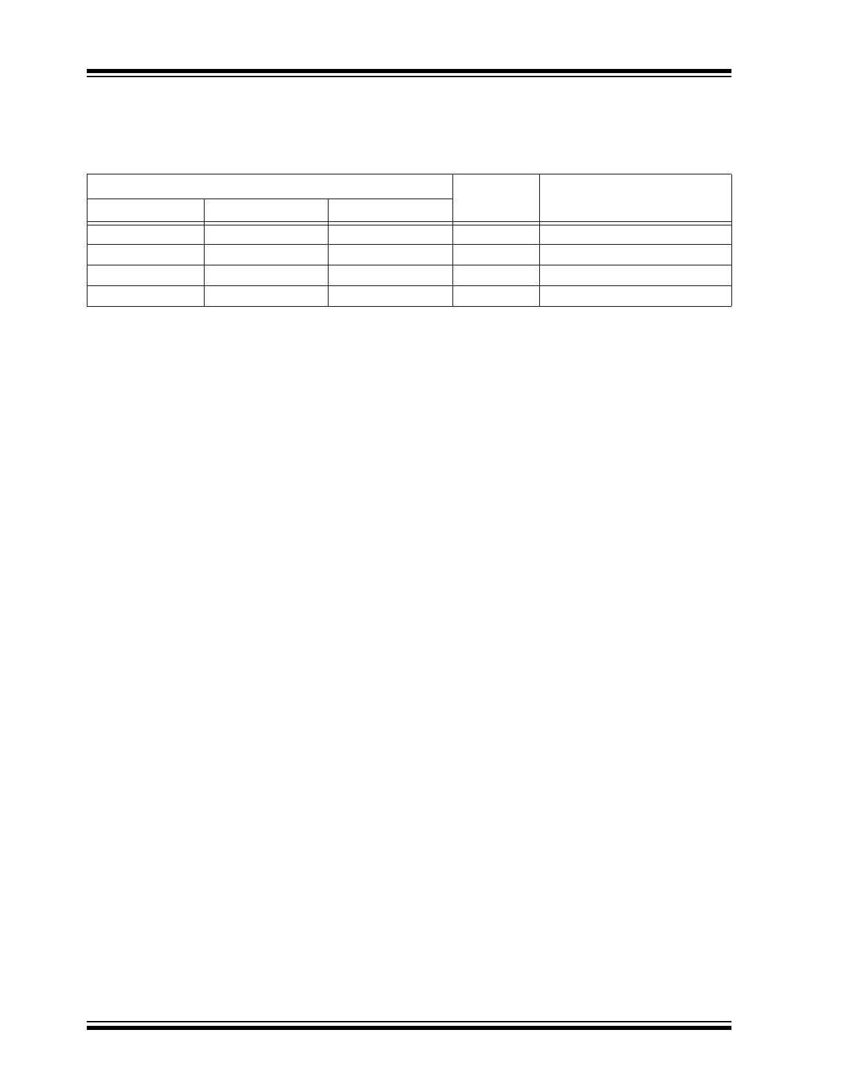
PIN DESCRIPTIONS
The descriptions of the pins are listed in
Table 2-1
.
TABLE 2-1:
PIN FUNCTION TABLE
2.1
Digital Output (V
OUT
)
V
OUT
goes low when V
IN
drops below V
DET
– and
returns high when V
IN
rises above V
DET
– + V
HYST
.
(See
Figure 3-1
).
2.2
Analog Input (V
IN
)
V
IN
can be used for power supply monitoring or a
voltage level that requires monitoring.
2.3
Ground Terminal (V
SS
)
V
SS
provides the negative reference for the analog
input voltage. Typically, the circuit ground is used.
TC54
Symbol
Description
SOT-23A
SOT-89
TO-92
1
1
1
V
OUT
Digital Output
3
2
2
V
IN
Analog Input
2
3
3
V
SS
Ground Terminal
—
Tab
—
V
IN
Analog Input
2001-2014 Microchip Technology Inc.
DS20001434K-page 5
TC54
3.0
DETAILED DESCRIPTION
In normal steady-state operation when V
IN
> V
DET
–,
the output will be at a logic-high (see
Figure 3-1
). In the
case of the TC54VN, this is an open-drain condition. If
the input falls below V
DET
–, the output will pull down
(Logic 0) to V
SS
. Generally, V
OUT
can pull down to
within 0.5V of V
SS
at rated output current and input
voltage. (See Section 1.0 “Electrical
Characteristics”).
The output (V
OUT
) will stay valid until the input voltage
falls below the minimum operating voltage (V
INMIN
) of
0.7V. Below this minimum operating voltage, the output
is undefined. During power-up (or anytime V
IN
has
fallen below V
INMIN
), V
OUT
will remain undefined until
V
IN
rises above V
INMIN
. When this occurs, the output
will become valid. V
OUT
will be in its Active-low state,
while V
INMIN
< V
IN
< V
DET
+ (therefore, V
DET
+ = V
DET
–
+ V
HYST
). If the input rises above V
DET
+, the output will
assume its Inactive state (high for TC54VC, open-drain
for TC54VN).
FIGURE 3-1:
Timing Diagram.
V
IN
Detect Voltage V
DET
–
Minimum Operating
Voltage
V
HYST
V
DET
+
Output Voltage
Release Voltage
or Reset Voltage
Ground Level
Ground Level
V
OUT
TC54
DS20001434K-page 6
2001-2014 Microchip Technology Inc.
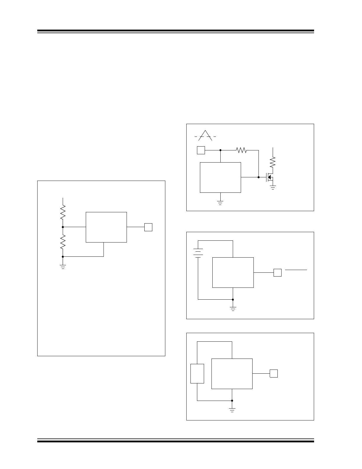
4.0
APPLICATIONS INFORMATION
4.1
Modifying the Trip Point, V
DET
–
Although the TC54 has a pre-programmed V
DET
–, it is
sometimes necessary to make adjustments during
prototyping. This can be accomplished by connecting
an external resistor divider to a TC54, which has a
V
DET
– lower than that of V
SOURCE
(
Figure 4-1
).
To maintain detector accuracy, the bleeder current
through the divider should be significantly higher than
the 1 µA operating current required by the TC54. A rea-
sonable value for this bleeder current is 100 µA (100
times the 1 µA required by the TC54). For example, if
V
DET
– = 2V and the desired trip point is 2.5V, the value
of R
1
+ R
2
is 25 k
(2.5V/100 µA). The value of
R
1
+ R
2
can be rounded to the nearest standard value
and plugged into the equation of
Figure 4-1
to calculate
values for R
1
and R
2
. 1% tolerance resistors are
recommended.
FIGURE 4-1:
Modify Trip-point of the
TC54 using External Resistor Divider.
4.2
Other Applications
Low operating power and small physical size make the
TC54 series ideal for many voltage detector applica-
tions, such as those shown in Figures
4-2
,
4-3
and
4-4
.
Figure 4-2
shows a low-voltage gate drive protection
circuit that prevents the overheating of the logic-level
MOSFET due to insufficient gate voltage. When the
input signal is below the threshold of the TC54VN, its
output grounds the gate of the MOSFET.
Figure 4-3
and
Figure
4-4
show the TC54 in conventional voltage
monitoring applications.
FIGURE 4-2:
MOSFET Low Drive
Protection.
FIGURE 4-3:
Battery Voltage Monitor.
FIGURE 4-4:
Power Good Monitor.
Note:
In this example, V
SOURCE
must be
greater than (V
DET
–)
V
SOURCE
R
1
R
1
R
2
+
--------------------
V
DET
-
=
V
IN
V
OUT
V
SS
R
1
V
SOURCE
R
2
Where:
V
SOURCE
= Voltage to be monitored
V
DET
– = Threshold Voltage setting of TC54
TC54
V
IN
V
OUT
V
SS
270
MTP3055EL
V
CC
R
L
4.3V
TC54VX
V
IN
V
OUT
V
SS
BATLOW
+
–
–
TC54VX
V
IN
V
OUT
V
SS
Power Good
+
–
Pwr.
Sply.
TC54VX
2001-2014 Microchip Technology Inc.
DS20001434K-page 7
TC54
5.0
PACKAGING INFORMATION
5.1
Package Marking Information
3-Lead SOT-23A
2NN
Example
C302
3-Lead SOT-89
XXXYYWW
@NNN
Example
E3
31
3-Lead TO-92
XXXXXX
XXXXXX
XXXXXX
YWWNNN
Example
54VN
3002
1256
Legend: XX...X
Customer-specific information
Y
Year code (last digit of calendar year)
YY
Year code (last 2 digits of calendar year)
WW
Week code (week of January 1 is week ‘01’)
NNN
Alphanumeric traceability code
Pb-free JEDEC
®
designator for Matte Tin (Sn)
*
This package is Pb-free. The Pb-free JEDEC designator ( )
can be found on the outer packaging for this package.
Note:
In the event the full Microchip part number cannot be marked on one line, it will
be carried over to the next line, thus limiting the number of available
characters for customer-specific information.
3
e
3
e
TC54
DS20001434K-page 8
2001-2014 Microchip Technology Inc.
)
Symbol
Output
Voltage
B
CMOS
1.
C
CMOS
2.
D
CMOS
3.
E
CMOS
4.
F
CMOS
5.
H
CMOS
6.
I
CMOS
7.
Symbol
Output
Voltage
L
N-Channel
1.
M
N-Channel
2.
N
N-Channel
3.
P
N-Channel
4.
R
N-Channel
5.
S
N-Channel
6.
T
N-Channel
7.
Symbol
Voltage
Symbol
Voltage
0
.0
6
.6
1
.1
7
.7
2
.2
8
.8
3
.3
9
.9
4
.4
5
.5
3-Pin SOT-23A
3-Pin SOT-89
1
1
2
2
4
3
4
3
1
represents output configuration (CMOS or Nch)
and first integer of voltage
Ex: CMOS 3.x =
D
2
represents first decimal of output voltage (0-9)
Ex: CMOS 3.x =
D 4
4
3
represent assembly lot code
and
Symbol
Output
C
CMOS
N
N-Channel
Symbol
Voltage
2
2.
3
3.
4
4.
5
5.
6
6.
Symbol
Voltage
Symbol
Voltage
0
.0
5
.5
1
.1
6
.6
2
.2
7
.7
3
.3
8
.8
4
.4
9
.9
Symbol
Delay Time
0
No Delay
Symbol
Accuracy
1
±1.0% (custom)
2
±2.0% (standard)
3-Pin TO-92
8
4
7
3
6
2
5
1
= 54X (fixed)
1 , 2 and
3
4
represents output configuration (CMOS or N-Ch)
Ex: CMOS 3.x =
C
5
represents first integer of detect voltage
6
represents first decimal of detect voltage
7
represents the output delay time
represents the device accuracy
8
2001-2014 Microchip Technology Inc.
DS20001434K-page 9
TC54
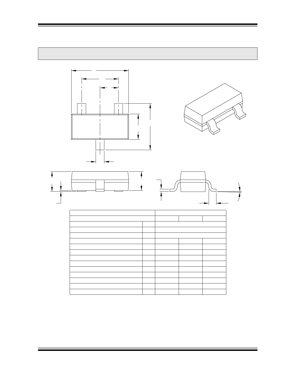
/HDG3ODVWLF6PDOO2XWOLQH7UDQVLVWRU&%>627$@
1RWHV
'LPHQVLRQV'DQG(GRQRWLQFOXGHPROGIODVKRUSURWUXVLRQV0ROGIODVKRUSURWUXVLRQVVKDOOQRWH[FHHGPPSHUVLGH
'LPHQVLRQLQJDQGWROHUDQFLQJSHU$60(<0
%6& %DVLF'LPHQVLRQ7KHRUHWLFDOO\H[DFWYDOXHVKRZQZLWKRXWWROHUDQFHV
1RWH
)RUWKHPRVWFXUUHQWSDFNDJHGUDZLQJVSOHDVHVHHWKH0LFURFKLS3DFNDJLQJ6SHFLILFDWLRQORFDWHGDW
KWWSZZZPLFURFKLSFRPSDFNDJLQJ
8QLWV0,//,0(7(56
'LPHQVLRQ/LPLWV
0,1
120
0$;
1XPEHURI3LQV1
/HDG3LWFK
H
%6&
2XWVLGH/HDG3LWFK
H
%6&
2YHUDOO+HLJKW
$
±
0ROGHG3DFNDJH7KLFNQHVV
$
±
6WDQGRII
$
±
2YHUDOO:LGWK
(
±
0ROGHG3DFNDJH:LGWK
(
±
2YHUDOO/HQJWK
'
±
)RRW/HQJWK
/
±
)RRW$QJOH
±
/HDG7KLFNQHVV
F
±
/HDG:LGWK
E
±
D
e
e1
2
1
E
E1
N
b
A
A1
A2
c
L
φ
0LFURFKLS 7HFKQRORJ\ 'UDZLQJ &%
TC54
DS20001434K-page 10
2001-2014 Microchip Technology Inc.
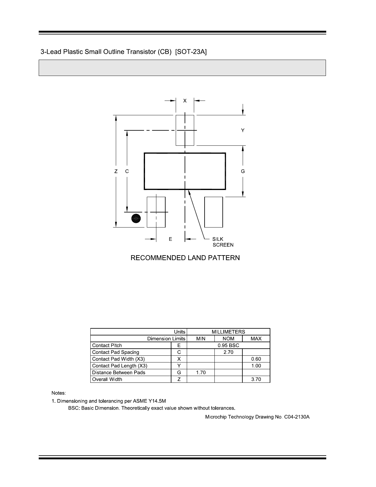
Note:
For the most current package drawings, please see the Microchip Packaging Specification located at
http://www.microchip.com/packaging