
2001-2011 Microchip Technology Inc.
DS21432D-page 1
TC53
Features:
• Highly Accurate: ±2%
• Low-Power Consumption: 1.0
A, Typ.
• Detect Voltage Range: 1.6V to 6.0V and 7.7V
• Operating Voltage: 1.5V to 10.0V
• Output Configuration: Open-Drain or CMOS
• Space-Saving 5-Pin SOT-23A Package
Typical Applications:
• Microprocessor Reset Circuits
• Battery Life Monitors and Recharge Voltage
Monitors
• Memory Battery Backup Circuitry
• Power-On Reset Circuits
• Power Failure Detection
• Delay Circuitry
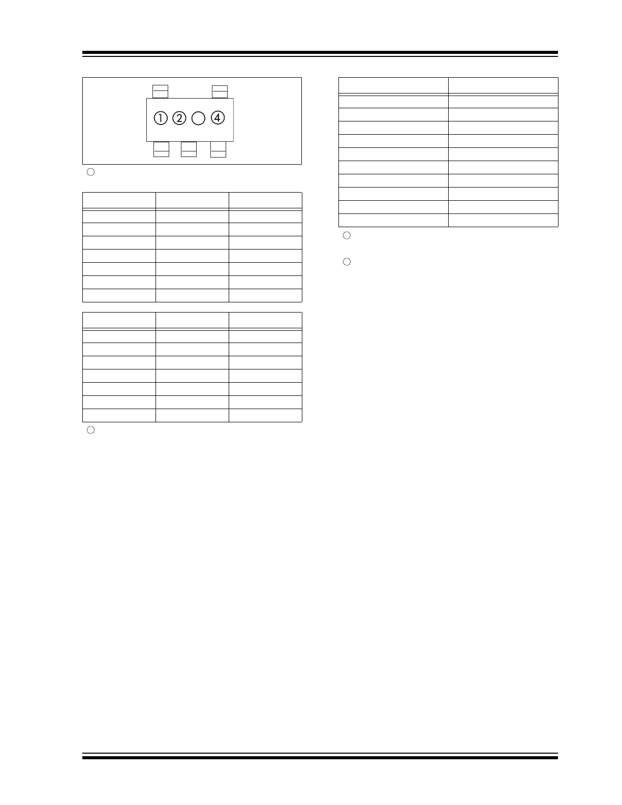
Device Selection Table
Other output voltages are available. Please contact
Microchip Technology Inc. for details.
Package Type
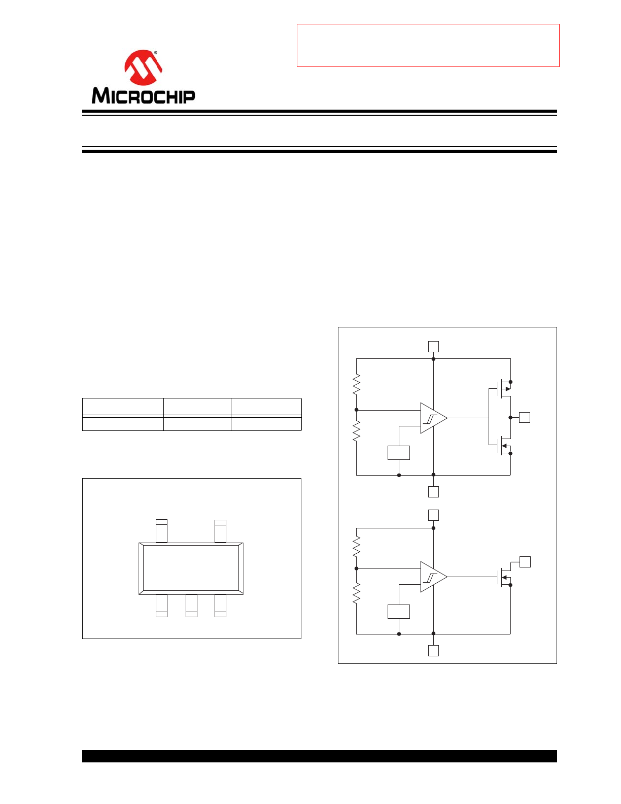
General Description:
The TC53 is a low-power voltage detector. Typical
supply current consumption is only 1
A at an input
voltage of 2V. The voltage detection threshold setting is
factory-programmed and ensured to ±2% accuracy.
Threshold settings are available over a range of 1.6V
to 6.0V. The TC53 has both complementary (CMOS)
and open drain (NMOS) output configuration options.
TC53 is the ideal voltage detector for precision
applications in which small size, low installed cost, high
accuracy and low supply current consumption are
critical.
Functional Block Diagram
Part Number
Package
Temp. Range
TC53-xxxxxxxxxx
5-Pin SOT-23A -40°C to +85°C
5
5-Pin SOT-23A
TC53
1
3
4
2
NC
V
OUT
V
IN
V
SS
NC
V
REF
V
SS
V
OUT
V
IN
V
REF
V
SS
V
OUT
V
IN
2) N-Channel
Open Drain Output
1) CMOS Output
Voltage Detector
Not recommended for new designs –
Please use MCP111/2
TC53
DS21432D-page 2
2001-2011 Microchip Technology Inc.
1.0
ELECTRICAL
CHARACTERISTICS
Absolute Maximum Ratings†
Input Voltage ........................................................+12V
Output Current ...................................................50 mA
Output Voltage.......................V
IN
+ 0.3V to V
SS
– 0.3V
Power Dissipation
5-Pin SOT-23A ..........................................240 mW
Operating Temperature Range............. -40°C to +85°C
Storage Temperature Range ..............-40°C to +125°C
†Stresses above those listed under “Absolute Maximum
Ratings” may cause permanent damage to the device. These
are stress ratings only and functional operation of the device
at these or any other conditions above those indicated in the
operation sections of the specifications is not implied.
Exposure to Absolute Maximum Rating conditions for
extended periods may affect device reliability.
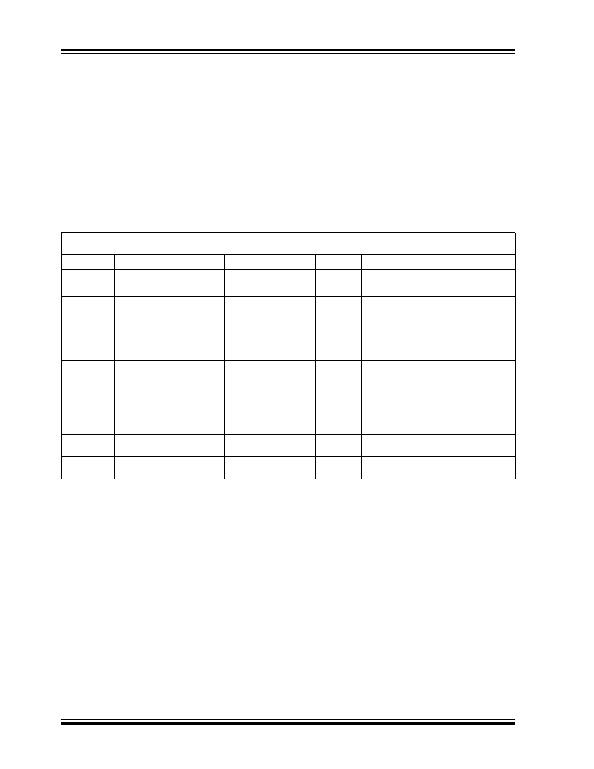
TC53 ELECTRICAL SPECIFICATIONS
Electrical Characteristics: T
A
= 25°C, unless otherwise specified.
Note 1
,
Note 2
.
Symbol
Parameter
Min
Typ
Max
Units
Test Conditions
V
DF
Detect Voltage
V
T
x 0.98
V
T
±0.5%
V
T
x 1.02
V
Note 3
V
HYS
Hysteresis Range
V
DF
x 0.02
V
DF
x 0.05
V
DF
x 0.08
V
I
SS
Supply Current
—
—
—
—
—
0.9
1.0
1.3
1.6
2.0
2.6
3.0
3.4
3.8
4.2
µA
V
IN
= 1.5V
V
IN
= 2.0V
V
IN
= 3.0V
V
IN
= 4.0V
V
IN
= 5.0V
V
IN
Operating Voltage
1.5
—
10.0
V
V
DF
= 2.1 to 6.0V
I
OUT
Output Current
—
—
—
—
—
2.2
7.7
10.1
11.5
13.0
—
—
—
—
—
mA
N-ch; V
DS
= 0.5V, V
IN
= 1.0V
V
IN
= 2.0V
V
IN
= 3.0V
V
IN
= 4.0V
V
IN
= 5.0V
—
-10.0
—
P-ch; V
DS
= 2.1V, V
IN
= 8.0V
(CMOS Output)
V
DF
/
(
T
OPR
V
DF
)
Temperature Characteristics
—
±100
—
ppm/°C
t
DLY
Delay Time
(V
DR
V
OUT
Inversion)
—
—
0.2
ms
Note
1:
An additional resistor between the V
IN
pin and the supply voltage may alter the electrical characteristics due to the increasing values of
V
DR
.
2:
The power consumption during power-start to output being stable (release operation) is 2
A greater than it is after that period
(completion of release operation) because of rush current in the delay circuit.
3:
V
T
is the factory-programmed voltage detection threshold.
2001-2011 Microchip Technology Inc.
DS21432D-page 3
TC53
2.0
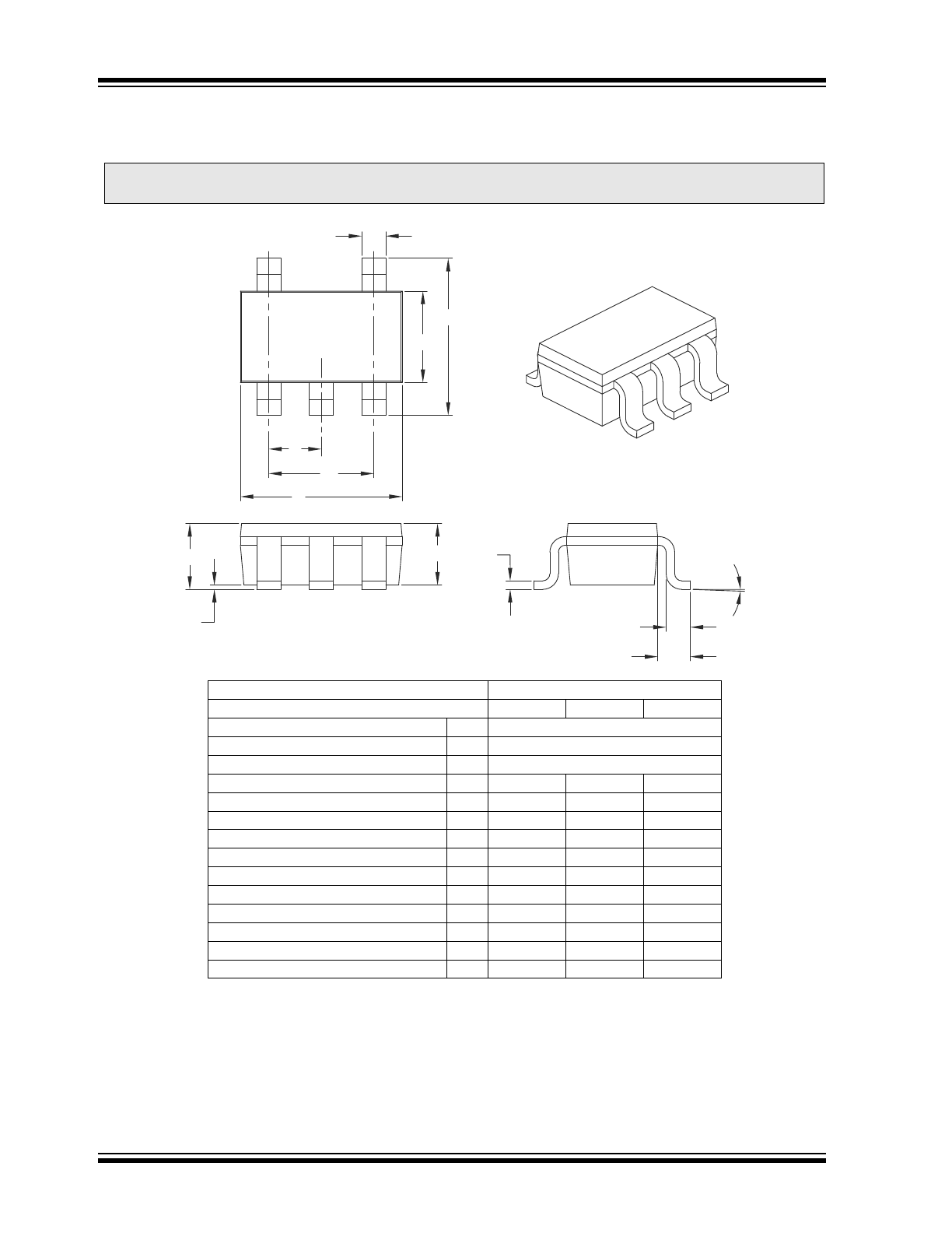
PIN DESCRIPTIONS
The descriptions of the pins are listed in
Table 2-1
.
TABLE 2-1:
PIN FUNCTION TABLE
3.0
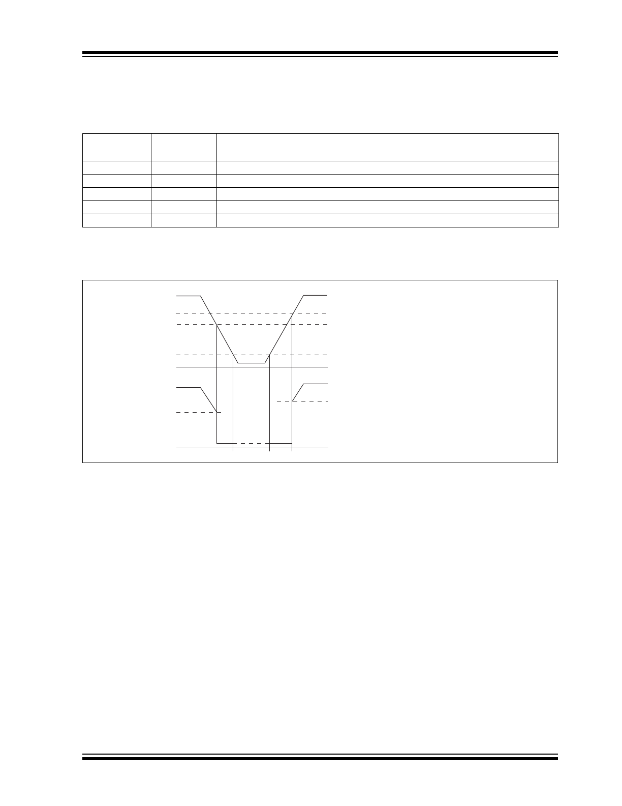
DETAILED DESCRIPTION
FIGURE 3-1:
TIMING DIAGRAM
Pin No.
(5-Pin SOT-23A)
Symbol
Description
1
V
OUT1
Output.
2
V
IN
Supply voltage input.
3
V
SS
Ground terminal.
4
NC
Not connected.
5
NC
Not connected.
Input Voltage (V
IN
)
Detect Release Voltage (V
DR
)
Detect Voltage (V
DF
)
Minimum Operating Voltage (V
MIN
)
Ground Voltage (V
SS
)
Output Voltage (V
OUT
)
Ground Voltage (V
SS
)
TC53
DS21432D-page 4
2001-2011 Microchip Technology Inc.
4.0
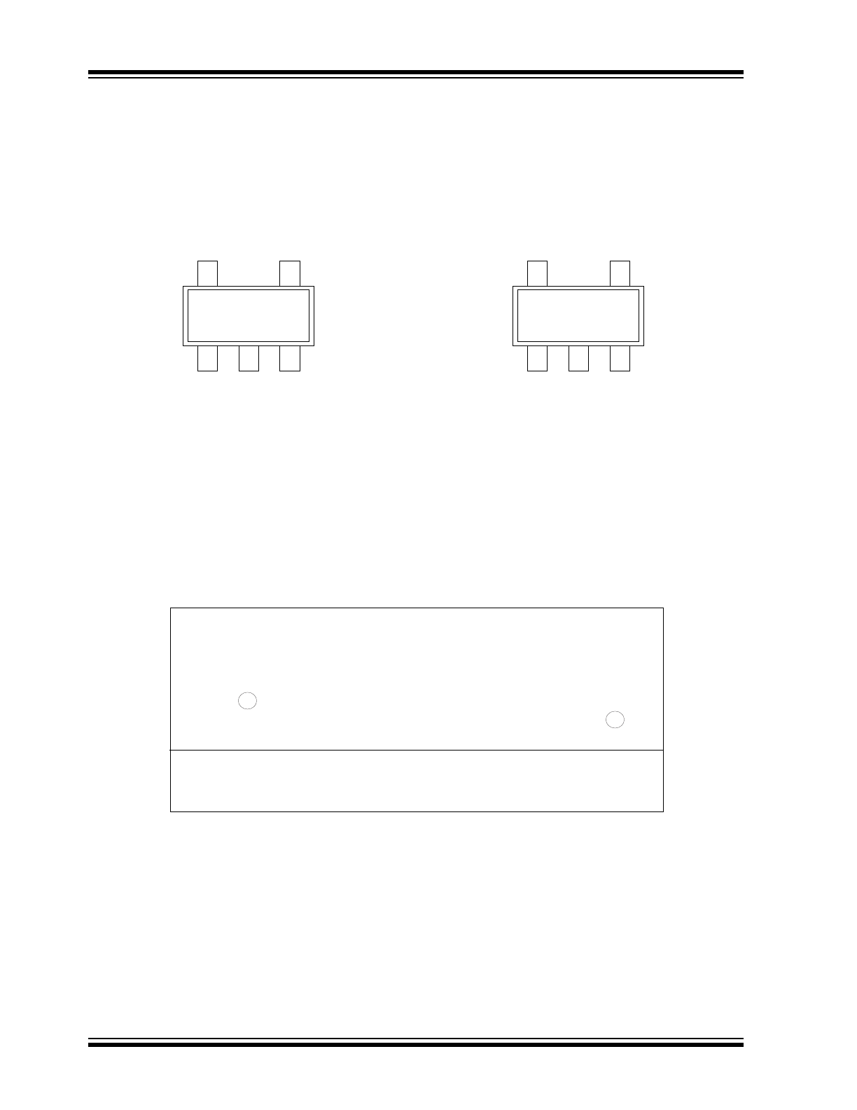
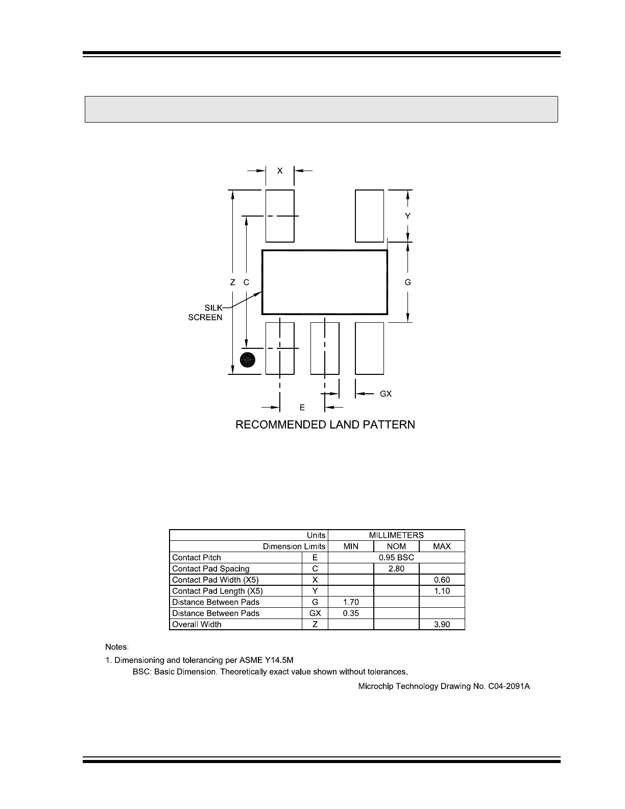
PACKAGING INFORMATION
4.1
Package Marking Information
Legend: XX...X
Customer-specific information
Y
Year code (last digit of calendar year)
YY
Year code (last 2 digits of calendar year)
WW
Week code (week of January 1 is week ‘01’)
NNN
Alphanumeric traceability code
Pb-free JEDEC designator for Matte Tin (Sn)
*
This package is Pb-free. The Pb-free JEDEC designator ( )
can be found on the outer packaging for this package.
Note:
In the event the full Microchip part number cannot be marked on one line, it will
be carried over to the next line, thus limiting the number of available
characters for customer-specific information.
3
e
3
e
5-Lead SOT-23A
XXNN
Example
L852
2001-2011 Microchip Technology Inc.
DS21432D-page 5
TC53
Symbol
Output
Voltage
A
CMOS
0.
B
CMOS
1.
C
CMOS
2.
D
CMOS
3.
E
CMOS
4.
F
CMOS
5.
H
CMOS
6.
Symbol
Output
Voltage
K
Nch
0.
L
Nch
1.
M
Nch
2.
N
Nch
3.
P
Nch
4.
R
Nch
5.
S
Nch
6.
3
1
represents output configuration and first integer
of voltage
2
represents first decimal of output voltage
Symbol
Voltage
0
.0
1
.1
2
.2
3
.3
4
.4
5
.5
6
.6
7
.7
8
.8
9
.9
4
represents assembly lot code
3
represents delay function and delay time
3 = no delay function
TC53
DS21432D-page 6
2001-2011 Microchip Technology Inc.
/HDG3ODVWLF6PDOO2XWOLQH7UDQVLVWRU&7>627@
1RWHV
'LPHQVLRQV'DQG(GRQRWLQFOXGHPROGIODVKRUSURWUXVLRQV0ROGIODVKRUSURWUXVLRQVVKDOOQRWH[FHHGPPSHUVLGH
'LPHQVLRQLQJDQGWROHUDQFLQJSHU$60(<0
%6& %DVLF'LPHQVLRQ7KHRUHWLFDOO\H[DFWYDOXHVKRZQZLWKRXWWROHUDQFHV
1RWH
)RUWKHPRVWFXUUHQWSDFNDJHGUDZLQJVSOHDVHVHHWKH0LFURFKLS3DFNDJLQJ6SHFLILFDWLRQORFDWHGDW
KWWSZZZPLFURFKLSFRPSDFNDJLQJ
8QLWV
0,//,0(7(56
'LPHQVLRQ/LPLWV
0,1
120
0$;
1XPEHURI3LQV
1
/HDG3LWFK
H
%6&
2XWVLGH/HDG3LWFK
H
%6&
2YHUDOO+HLJKW
$
±
0ROGHG3DFNDJH7KLFNQHVV
$
±
6WDQGRII
$
±
2YHUDOO:LGWK
(
±
0ROGHG3DFNDJH:LGWK
(
±
2YHUDOO/HQJWK
'
±
)RRW/HQJWK
/
±
)RRWSULQW
/
±
)RRW$QJOH
±
/HDG7KLFNQHVV
F
±
/HDG:LGWK
E
±
φ
N
b
E
E1
D
1
2
3
e
e1
A
A1
A2
c
L
L1
0LFURFKLS 7HFKQRORJ\ 'UDZLQJ &%
2001-2011 Microchip Technology Inc.
DS21432D-page 7
TC53
5-Lead Plastic Small Outline Transistor (CT) [SOT-23]
Note:
For the most current package drawings, please see the Microchip Packaging Specification located at
http://www.microchip.com/packaging

TC53
DS21432D-page 8
2001-2011 Microchip Technology Inc.
NOTES:

2001-2011 Microchip Technology Inc.
DS21432D-page 9
TC53
APPENDIX A:
REVISION HISTORY
Revision D (August 2011)
• Changed status from active to end-of-life (EOL)
Revision C (July 2002
• Undocumented changes
Revision B (May 2002)
• Undocumented changes
Revision A (March 2001)
• Original Release of this Document.

TC53
DS21432D-page 10
2001-2011 Microchip Technology Inc.
NOTES: