
2001-2015 Microchip Technology Inc.
DS20001430E-page 1
TC52
Features
• Two Independent Voltage Detectors in One
Package
• Highly Accurate: ±2%
• Low Power Consumption: 2.0 μA, typical
• Channel 1 Detect Voltage: 3.0V, 4.5V
• Channel 2 Detect Voltage: 2.7V
• Operating Voltage: 1.5V to 10.0V
• Output Configuration: N-Channel Open-Drain
• Space-Saving 5-Pin SOT-23 Package
Typical Applications
• Battery Life Monitors and Recharge Voltage
Monitors
• Memory Battery Backup Circuitry
• Power-On Reset Circuits
• Power Failure Detection
• Delay Circuitry
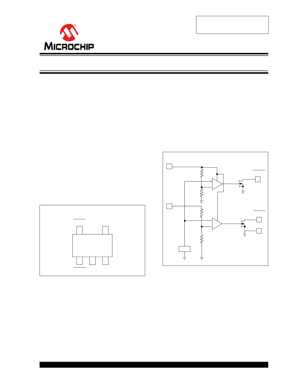
Package Type
Description
The TC52 consists of two independent low-power
voltage detectors in a space-saving 5-pin SOT-23
package. Typical supply current consumption is only
2 μA at an input voltage of 2V. The voltage detection
threshold settings are factory-programmed and
guaranteed to ±2% accuracy. The TC52 is available
with open drain (NMOS) configurations. Small-size,
high-precision, low-supply current, and low installed
cost makes the TC52 the ideal voltage detector for a
wide variety of voltage monitoring applications.
Functional Block Diagram
5-Pin SOT-23
1
2
3
5
4
V
IN1
V
IN2
GND
V
OUT2
V
OUT1
+
–
+
–
V
IN1
V
IN2
V
REF
V
OUT1
V
OUT2
GND
Dual-Channel Voltage Detector
Obsolete Device
TC52
DS20001430E-page 2
2001-2015 Microchip Technology Inc.
1.0
ELECTRICAL
CHARACTERISTICS
Absolute Maximum Ratings*
Input Voltage ........................................................+12V
Output Current ...................................................50 mA
Output Voltage.......................V
IN
+ 0.3V to V
SS
– 0.3V
Power Dissipation
5-Pin SOT-23 ............................................100 mW
Operating Temperature Range.............-40°C to +85°C
Storage Temperature Range ..............-40°C to +125°C
† Notice:
Stresses above those listed under "Absolute
Maximum Ratings" may cause permanent damage to
the device. These are stress ratings only and functional
operation of the device at these or any other conditions
above those indicated in the operation sections of the
specifications is not implied. Exposure to Absolute
Maximum Rating conditions for extended periods may
affect device reliability.
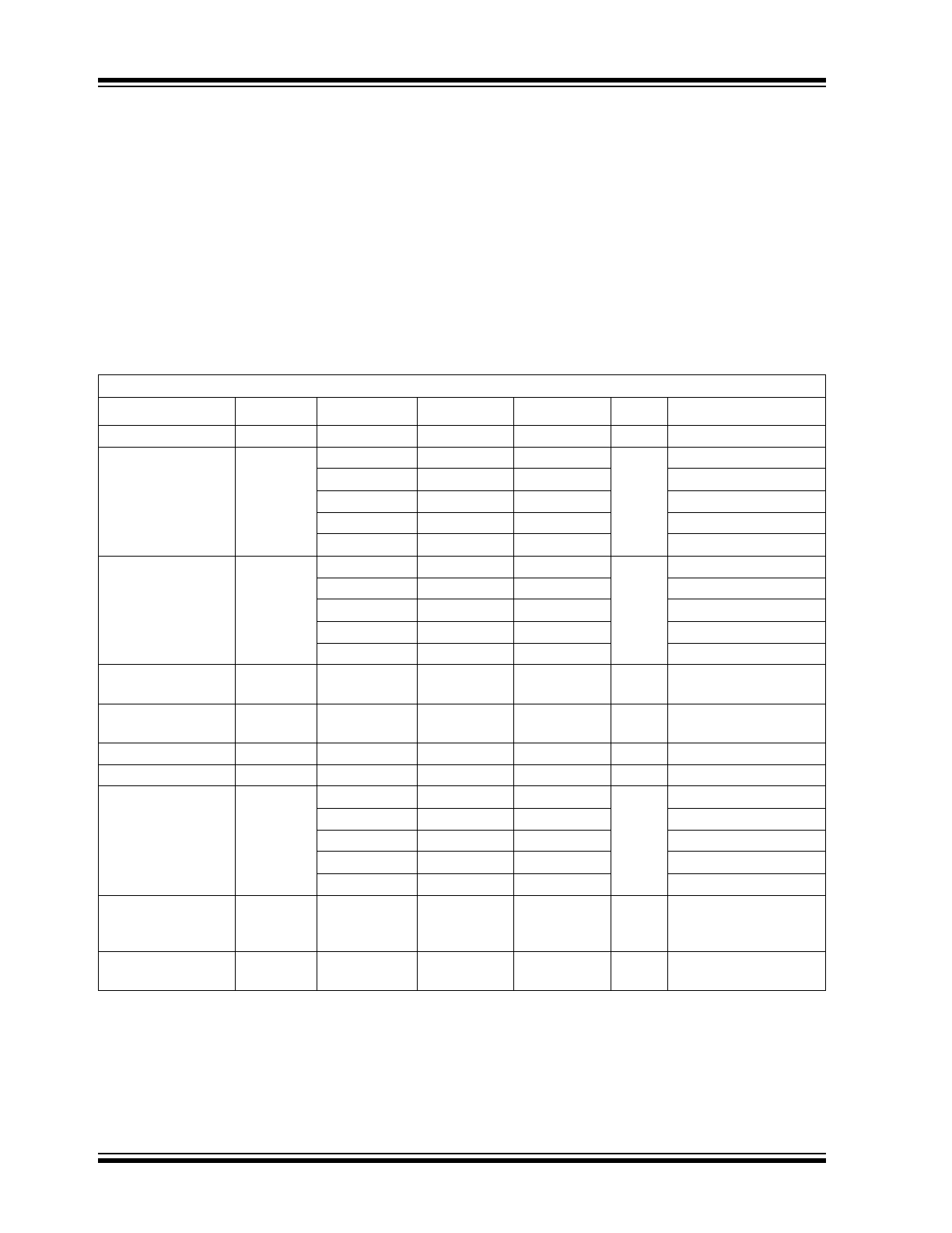
DC ELECTRICAL CHARACTERISTICS
Electrical Specifications:
T
A
= 25°C, unless otherwise specified. Note 1.
Parameter
Sym.
Min.
Typ.
Max.
Units
Conditions
Operating Voltage
V
IN
1.5
—
10.0
V
V
DF
(T) = 1.5 to 5.0V
Supply Current
I
SS
—
1.35
3.90
μA
V
IN1
= 1.5V
—
1.50
4.50
V
IN1
= 2.0V
—
1.95
5.10
V
IN1
= 3.0V
—
2.40
5.70
V
IN1
= 4.0V
—
3.00
6.30
V
IN1
= 5.0V
Input Current V
IN2
I
IN2
—
0.45
1.30
μA
V
IN1
= 1.5V
—
0.50
1.50
V
IN1
= 2.0V
—
0.65
1.70
V
IN1
= 3.0V
—
0.80
1.90
V
IN1
= 4.0V
—
1.00
2.10
V
IN1
= 5.0V
Channel 1
Detect Voltage
V
DET1
-
V
T1
x 0.98
V
T1
± 0.5%
V
T1
x 1.02
V
Note 2
Channel 2
Detect Voltage
V
DET2
-
V
T2
x 0.98
V
T2
± 0.5%
V
T2
x 1.02
V
Note 2
Hysteresis Range 1
V
HYS1
V
DET1
- x 0.02 V
DET1
- x 0.05 V
DET1
- x 0.08
V
Hysteresis Range 2
V
HYS2
V
DET2
- x 0.02 V
DET2
- x 0.05 V
DET2
- x 0.08
V
Output Current
I
OUT
0.3
2.2
—
mA
V
OL
= 0.5V, V
IN1
= 1.0V
3.0
7.7
—
V
OL
= 0.5V, V
IN1
= 2.0V
5.0
10.1
—
V
OL
= 0.5V, V
IN1
= 3.0V
6.0
11.5
—
V
OL
= 0.5V, V
IN1
= 4.0V
7.0
13.0
—
V
OL
= 0.5V, V
IN1
= 5.0V
Temperature
Characteristics
ΔV
DET
-/
(
ΔT
OPR
V
DET
-)
—
±100
—
ppm/°C -40°C
≤ T
OPR
≤ 85°C
Detection Time
t
DLY
—
—
0.2
msec
Time from V
IN
= V
DET
-
to V
OUT
= V
OL
Note 1:
Additional resistance between the V
IN1
pin and the supply voltage may alter the electrical characteristics.
2:
V
T1
, V
T2
are the factory-programmed voltage detection thresholds.
2001-2015 Microchip Technology Inc.
DS20001430E-page 3
TC52
2.0
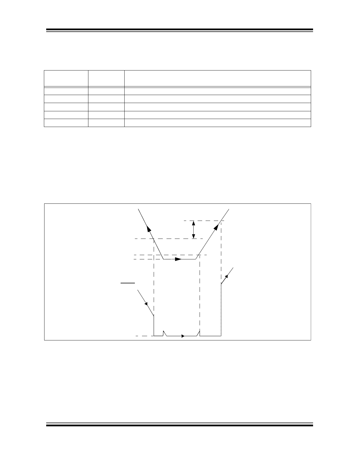
PIN DESCRIPTIONS
The descriptions of the pins are listed in
Table 2-1
.
3.0
DETAILED DESCRIPTION
In normal steady-state operation and for either
channel, when V
IN
> V
DET
-, the output is high, see
Figure 3-1
. (In the case of the TC52N, this is an open-
drain condition.) If and when the input falls below
V
DET
-, the output pulls down (Logic 0) to V
SS
.
Generally, V
OUT
can pull down to within 0.5V of V
SS
at
rated output current and input voltages. (Also see
Section 1.0, Electrical Characteristics
).
The output, V
OUT
, stays valid until the input voltage falls
below the minimum operating voltage, V
IN
MIN
, of 0.7V.
Below this minimum operating voltage, the output is
undefined. During power-up or anytime V
IN
has fallen
below V
IN
MIN
, V
OUT
will remain undefined until V
IN
rises
above V
IN
MIN
, at which time the output becomes valid.
V
OUT
is maintained in its active low state while
V
IN
MIN
< V
IN
< V
DET
+. (V
DET
+ = V
DET
- + V
HYST
). If and
when the input rises above V
DET
+, the output will
assume its inactive state (open-drain for TC52N).
FIGURE 3-1:
Timing Diagram.
TABLE 2-1:
PIN FUNCTION TABLE
Pin No.
(5-Pin SOT-23)
Symbol
Description
1
V
OUT1
Detector #1 output
2
V
IN
Supply voltage input, detect voltage 1
3
GND
Ground terminal
4
V
IN2
Detect voltage 2
5
V
OUT2
Detector #2 output
V
INx
Detect Voltage V
DET
–
Minimum Operating
Voltage
Ground Level
V
OUTx
Output Voltage
Ground Level
V
DET
+
V
HYST
Release Voltage
or RESET Voltage

TC52
DS20001430E-page 4
2001-2015 Microchip Technology Inc.
4.0
APPLICATION INFORMATION
Pin 2 (V
IN1
) acts as both the input to Voltage Detector
#1 and the power supply input for the chip. As such,
always assign V
IN1
to monitor voltages between 1.5V
and 10V. Failure to do this will result in unreliable
detector operation due to an out-of-tolerance supply
voltage. In high-noise environments, it may be
necessary to install a small input bypass capacitor
(0.01 μF to 0.1 μF) from V
IN1
to ground to minimize on-
chip power supply noise.
2001-2015 Microchip Technology Inc.
DS20001430E-page 5
TC52
5.0
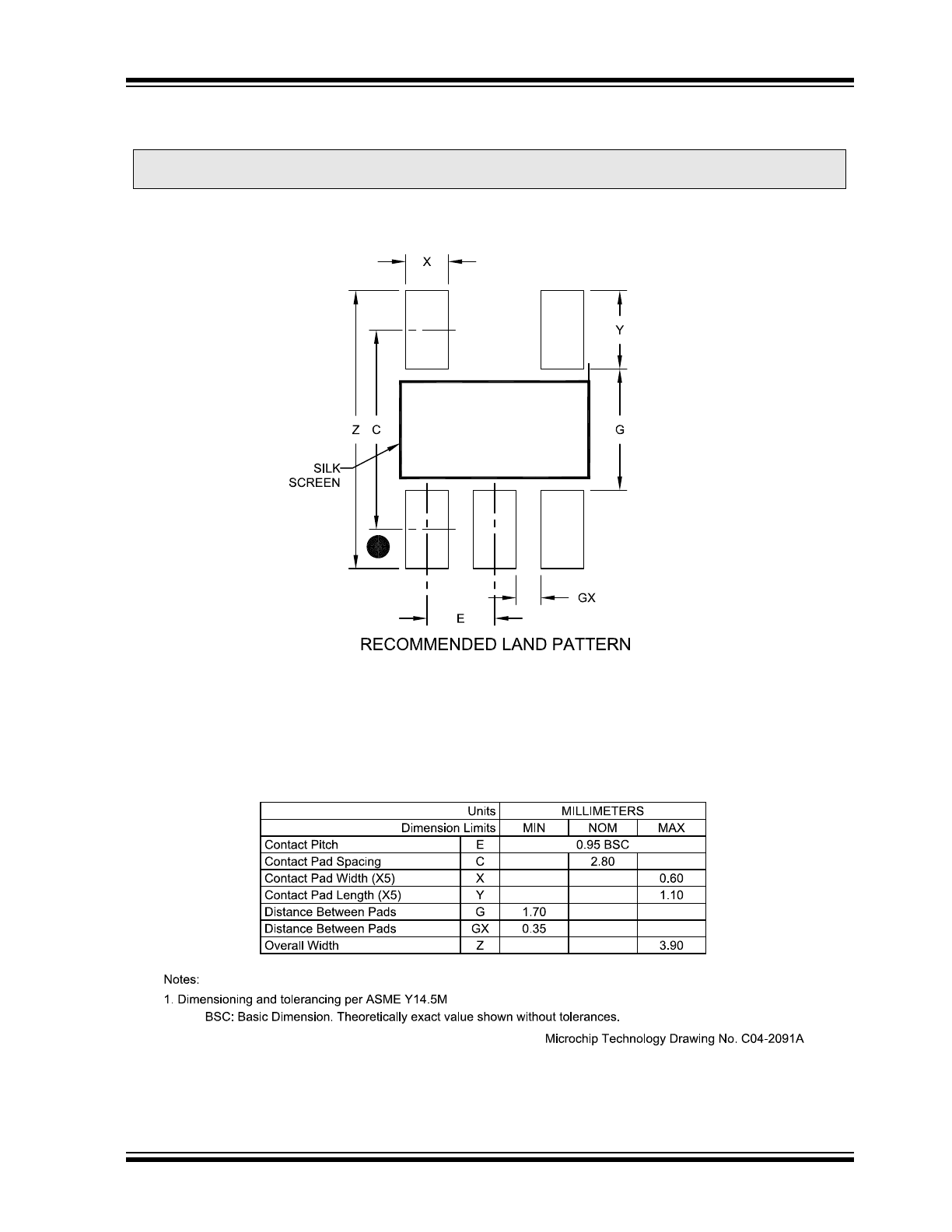
PACKAGING INFORMATION
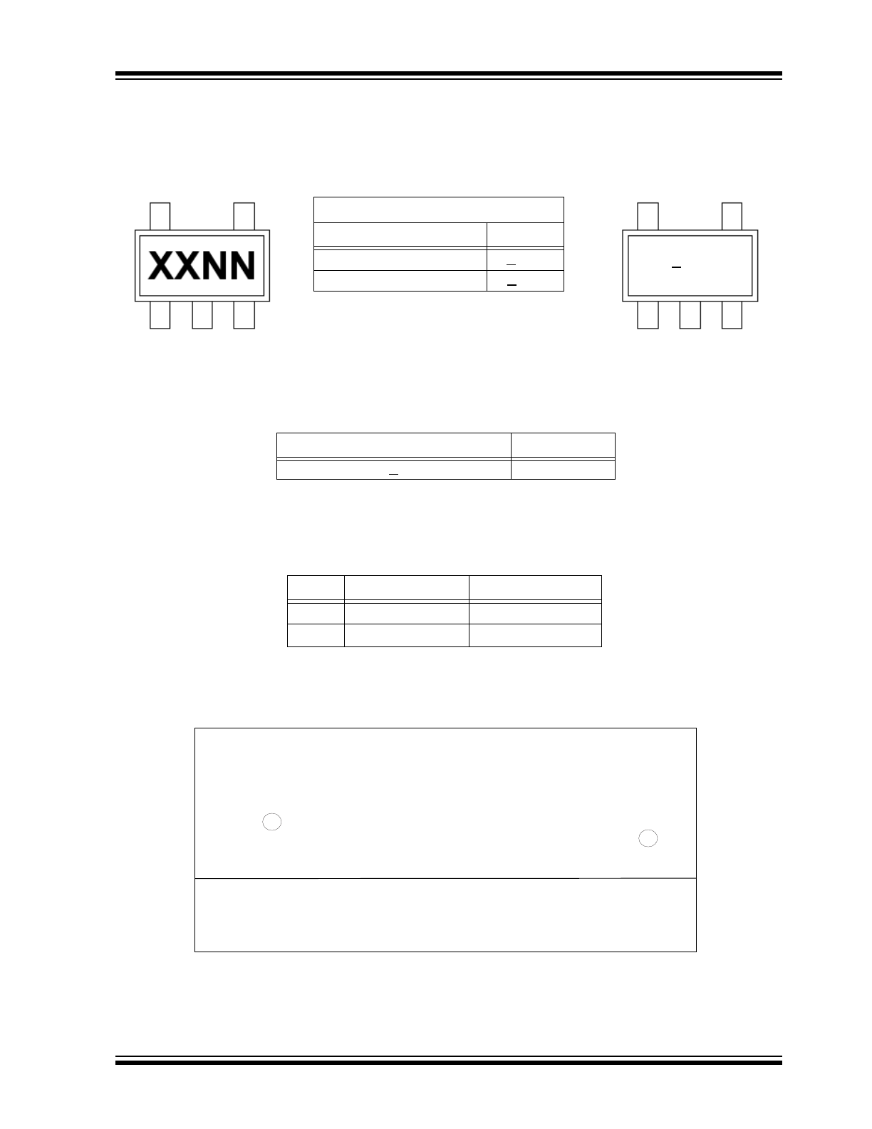
5.1
Package Marking Information
5-Lead SOT-23
Example
N0C2
Standard Markings for SOT-23
Part Number
Code
TC52N3027ECTTR
N0C#
TC52N4527ECTTR
N0P#
Note
:
In the event the full Microchip part number cannot be marked on one line, it will
be carried over to the next line, thus limiting the number of available
characters for customer-specific information.
Legend:
XX...X
Customer-specific information
Y
Year code (last digit of calendar year)
YY
Year code (last 2 digits of calendar year)
WW
Week code (week of January 1 is week ‘01’)
NNN
Alphanumeric traceability code
Pb-free JEDEC designator for Matte Tin (Sn)
*
This package is Pb-free. The Pb-free JEDEC designator ( )
can be found on the outer packaging for this package.
3
e
3
e
N-channel Indication and Integer Part of Output Voltage
Symbol
Output
N
Nch
Registration Serial Number
Symbol Detected Voltage 1
Detected Voltage 2
0C
3.0
2.7
0P
4.5
2.7
TC52
DS20001430E-page 6
2001-2015 Microchip Technology Inc.
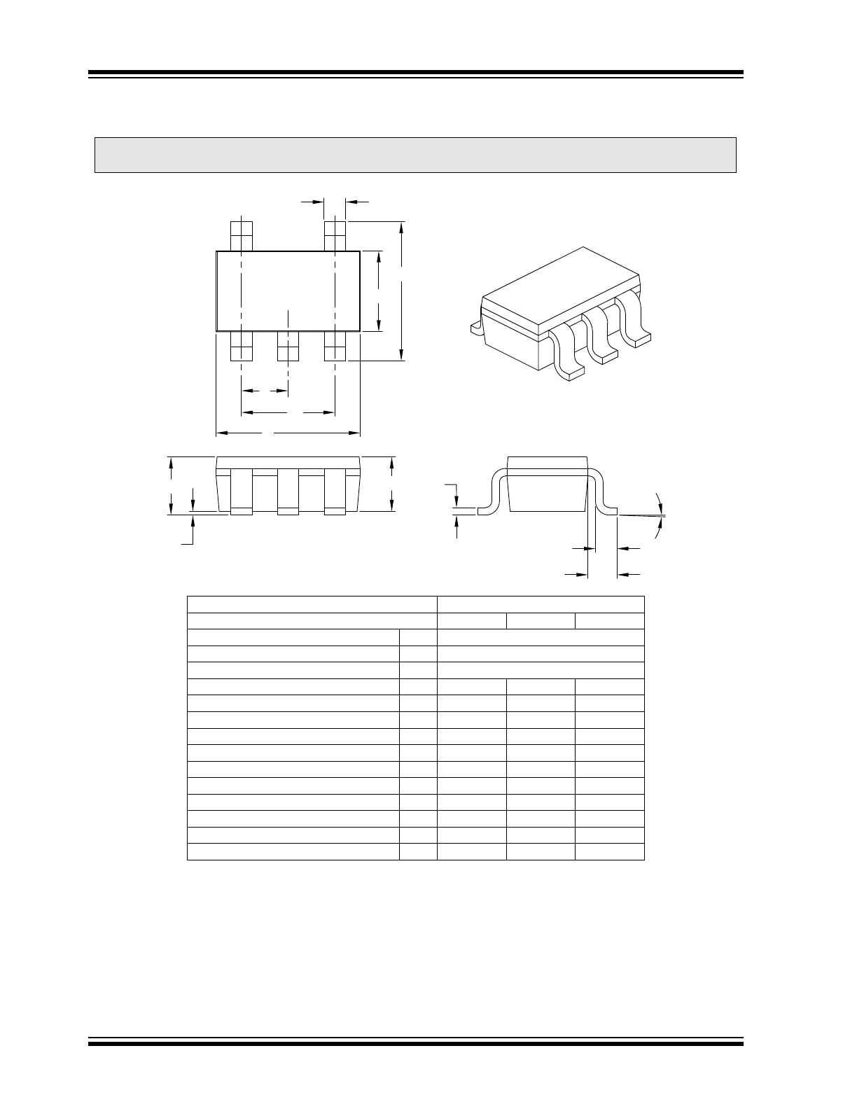
/HDG3ODVWLF6PDOO2XWOLQH7UDQVLVWRU&7>627@
1RWHV
'LPHQVLRQV'DQG(GRQRWLQFOXGHPROGIODVKRUSURWUXVLRQV0ROGIODVKRUSURWUXVLRQVVKDOOQRWH[FHHGPPSHUVLGH
'LPHQVLRQLQJDQGWROHUDQFLQJSHU$60(<0
%6& %DVLF'LPHQVLRQ7KHRUHWLFDOO\H[DFWYDOXHVKRZQZLWKRXWWROHUDQFHV
1RWH
)RUWKHPRVWFXUUHQWSDFNDJHGUDZLQJVSOHDVHVHHWKH0LFURFKLS3DFNDJLQJ6SHFLILFDWLRQORFDWHGDW
KWWSZZZPLFURFKLSFRPSDFNDJLQJ
8QLWV
0,//,0(7(56
'LPHQVLRQ/LPLWV
0,1
120
0$;
1XPEHURI3LQV
1
/HDG3LWFK
H
%6&
2XWVLGH/HDG3LWFK
H
%6&
2YHUDOO+HLJKW
$
±
0ROGHG3DFNDJH7KLFNQHVV
$
±
6WDQGRII
$
±
2YHUDOO:LGWK
(
±
0ROGHG3DFNDJH:LGWK
(
±
2YHUDOO/HQJWK
'
±
)RRW/HQJWK
/
±
)RRWSULQW
/
±
)RRW$QJOH
I
±
/HDG7KLFNQHVV
F
±
/HDG:LGWK
E
±
φ
N
b
E
E1
D
1
2
3
e
e1
A
A1
A2
c
L
L1
0LFURFKLS 7HFKQRORJ\ 'UDZLQJ &%
2001-2015 Microchip Technology Inc.
DS20001430E-page 7
TC52
5-Lead Plastic Small Outline Transistor (CT) [SOT-23]
Note:
For the most current package drawings, please see the Microchip Packaging Specification located at
http://www.microchip.com/packaging

TC52
DS20001430E-page 8
2001-2015 Microchip Technology Inc.
NOTES:

2001-2015 Microchip Technology Inc.
DS20001430E-page 9
TC52
APPENDIX A:
REVISION HISTORY
Revision E (February 2015)
• Updated device status to Obsolete.
Revision D (August 2013)
The following is the list of modifications:
1.
Updated the detect voltage values in
“Features”
.
2.
Updated the
“Package Type”
drawing.
3.
Updated
Section 5.0, "Packaging Informa-
tion"
with the latest package specification draw-
ings.
4.
Updated the
"Product Identification System"
section.
Revision C (December 2012)
• Added a note to each package outline drawing.
Revision B (May 2002)
• Undocumented changes.
Revision A (March 2001)
• Original Release of this Document.

2001-2015 Microchip Technology Inc.
DS20001430E-page 10
TC52
PRODUCT IDENTIFICATION SYSTEM
To order or obtain information, e.g., on pricing or delivery, refer to the factory or the listed sales office
.
PART NO.
-X
XX
Package
Temperature
Range
Device
Device:
TC52N3027ECTTR: 3.0V and 2.7V Dual Channel Voltage
Detector (Tape and Reel)
TC52N4527ECTTR: 4.5V and 2.7V Dual Channel Voltage
Detector (Tape and Reel)
Output Configuration:
N = Open Drain
Detected Voltage 1:
30 = 3.0V
45 = 4.5V
Detected Voltage 2:
27 = 2.7V
Temperature Range:
E = -40
°C to +125°C
Package:
CT = Plastic Small Outline Transistor (CT), 5-Lead
Examples:
a) TC52N3027ECTTR: 3.0V and 2.7V
Dual Channel Voltage Detector,
5LD SOT-23 package,
Tape and Reel
b) TC52N4527ECTTR: 4.5V and 2.7V
Dual Channel Voltage Detector,
5LD SOT-23 package,
Tape and Reel
XX
Tape and Reel
XX
Detected
Voltage 1
XX
Detected
Voltage 2
X
Output
Configuration