
2001-2014 Microchip Technology Inc.
DS20001426D-page 1
TC4626/TC4627
Features:
• Power Driver With On-Board Voltage Booster
• Low I
DD
: < 4 mA
• Small Package: 8-Pin PDIP
• Undervoltage Circuitry
• Fast Rise/Fall Time: <40 ns @1000 pF
• Below-Rail Input Protection
Applications:
• Raises 5V to drive higher – Vgs (ON) MOSFETs
• Eliminates one system power supply
General Description:
The TC4626/TC4627 are single CMOS high-speed
drivers with an on-board voltage boost circuit. These
parts work with an input supply voltage from 4 to 6 volts.
The internal voltage booster will produce a V
BOOST
potential up to 12 volts above V
IN
. This V
BOOST
is not
regulated, so its voltage is dependent on the input V
DD
voltage and output drive loading requirements. An
internal undervoltage lockout circuit keeps the output in
a low state when V
BOOST
drops below 7.8 volts. Output
is enabled when V
BOOST
is above 11.3 volts.
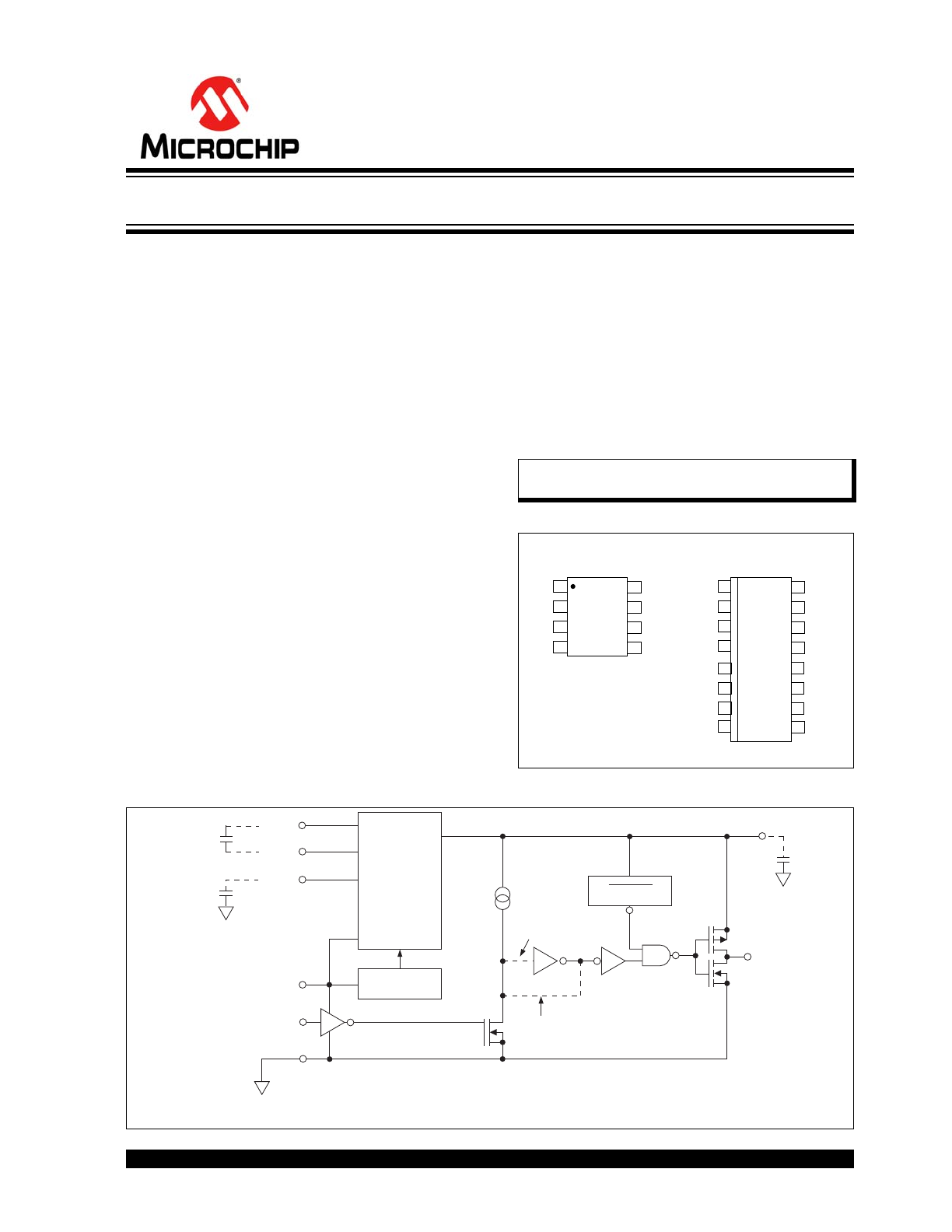
Package Type
Functional Block Diagram
Note:
Check the Microchip web site for available
package types and package information.
C2
C1
+
GND
1
2
3
4
8
7
6
5
C1
-
V
DD
IN
V
BOOST
OUT
C1
+
NC
IN
1
2
3
4
16
15
14
13
C1
-
NC
V
DD
NC
NC
12
11
10
5
6
7
NC
NC
C2
NC
V
BOOST
NC
PDIP/CERDIP
SOIC
8
9
GND
OUT
TC4626
TC4627
TC4626
TC4627
Voltage
Booster
Clock
C1+
C1-
C2
I
0
GND
EXT
Output
V
BOOST
EXT
V = 2 x V
DD
V
DD
1
2
3
8
7
4
6
5
C
3
Noninverting
4#
Inverting
4#
(Unregulated 3 x V
DD
)
UV LOCK
C
2
EXT
C
1
+
+
+
NOTE: Pin numbers correspond to 8-pin package.
Power CMOS Drivers With Voltage Tripler
TC4626/TC4627
DS20001426D-page 2
2001-2014 Microchip Technology Inc.
1.0
ELECTRICAL
CHARACTERISTICS
Absolute Maximum Ratings†
Supply Voltage ......................................................6.2V
Input Voltage, Any Terminal
..................................... V
S
+ 0.3V to GND – 0.3V
Package Power Dissipation (T
A
70°C)
PDIP........................................................730 mW
CERDIP...................................................800 mW
SOIC .......................................................760 mW
Derating Factor PDIP .......5.6 mW/°C Above 36°C
CERDIP...............................................6.0 mW/°C
Operating Temperature Range (Ambient)
C Version......................................... 0°C to +70°C
E Version......................................-40°C to +85°C
M Version ...................................-55°C to +125°C
Storage Temperature Range ..............-65°C to +150°C
† Notice
: Stresses above those listed under “Absolute Maxi-
mum Ratings” may cause permanent damage to the device.
These are stress ratings only and functional operation of the
device at these or any other conditions above those indicated
in the operation sections of the specifications is not implied.
Exposure to Absolute Maximum Rating conditions for
extended periods may affect device reliability.
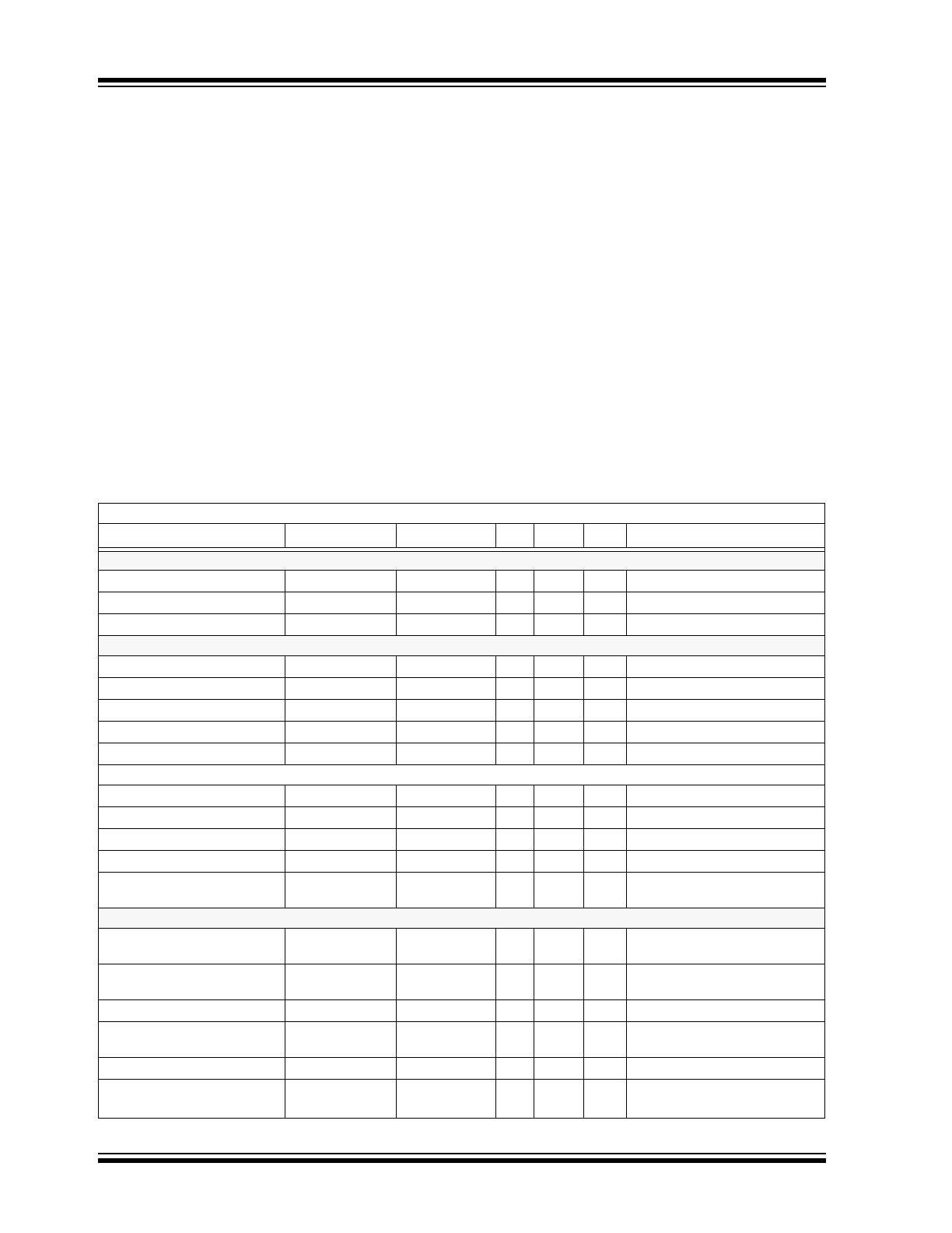
TC4626/TC4627 ELECTRICAL SPECIFICATIONS
Electrical Characteristics:
T
A
= +25°C, V
DD
= 5V, C
1
= C
2
= C
3
10µF unless otherwise noted.
Parameter
Symbol
Min.
Typ.
Max.
Units
Test Conditions
Input
Logic ‘1’, High Input Voltage
V
IH
2.4
—
—
V
Logic ‘0’, Low Input Voltage
V
IL
—
—
0.8
V
Input Current
I
IN
-1
—
+1
µA
0V
V
IN
V
DRIVE
Output
High Output Voltage
V
OH
V
BOOST
– 0.025
—
—
V
Low Output Voltage
V
OL
—
—
0.025
V
Output Resistance, High
R
O
—
10
15
Ω
I
OUT
= 10 mA, V
DD
= 5V
Output Resistance, Low
R
O
—
8
10
Ω
I
OUT
= 10 mA, V
DD
= 5V
Peak Output Current
I
PK
—
1.5
—
A
Switching Time
Rise Time
t
R
—
33
40
ns
Figure 3-1
,
Figure 3-2
Fall Time
t
F
—
27
35
ns
Figure 3-1
,
Figure 3-2
Delay Time
t
D1
—
35
45
ns
Figure 3-1
,
Figure 3-2
Delay Time
t
D2
—
45
55
ns
Figure 3-1
,
Figure 3-2
Maximum Switching Frequency
F
MAX
1.0
—
—
MHz V
DD
= 5V, V
BOOST
> 8.5V,
Figure 3-1
Voltage Booster
Voltage Tripler Output
Source Resistance
R
3
—
300
400
Ω
I
L
= 10mA, V
DD
= 5V
Voltage Doubler Output
Source Resistance
R
2
—
120
200
Ω
Oscillator Frequency
F
OSC
12
—
28
kHz
Oscillator Amplitude Measured
at C1-
V
OSC
4.5
—
10
V
R
LOAD
= 10 kΩ
Undervoltage Threshold
UV @V
BOOST
7.0
7.8
8.5
V
Start-Up Voltage
V
START
@V
BOOST
10.5
11.3
12
V
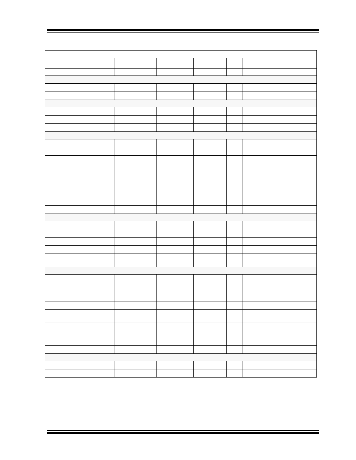
2001-2014 Microchip Technology Inc.
DS20001426D-page 3
TC4626/TC4627
@V
DD
= 5V
V
BOOST
14.6
—
—
V
No Load
Power Supply
Power Supply Current
I
DD
—
—
2.5
mA
V
IN
= Low or High
Supply Voltage
V
DD
4.0
—
6.0
V
Input
Logic 1, High Input Voltage
V
IH
2.4
—
—
V
Logic 0, Low Input Voltage
V
IL
—
—
0.8
V
Input Current
I
IN
-10
—
1
µA
0V
V
IN
V
BOOST
Output
High Output Voltage
V
OH
V
DRIVE
– 0.025
—
—
V
Low Output Voltage
V
OL
—
—
0.025
V
Output Resistance, High
R
O
—
15
15
20
25
Ω
I
OUT
= 10 mA, V
DD
= 5V
C & E Version
(T
A
= +70°C or +85°C)
M Version (T
A
= +125°C)
Output Resistance, Low
R
O
—
10
10
13
15
Ω
I
OUT
= 10 mA, V
DD
= 5V
C & E Version
(T
A
= +70°C or +85°C)
M Version (T
A
= +125°C)
Peak Output Current
I
PK
—
1.5
—
A
Switching Time
Rise Time
t
R
—
—
55
ns
Figure 3-1
,
Figure 3-2
Fall Time
t
F
—
—
50
ns
Figure 3-1
,
Figure 3-2
Delay Time
t
D1
—
—
60
ns
Figure 3-1
,
Figure 3-2
Delay Time
t
D2
—
—
70
ns
Figure 3-1
,
Figure 3-2
Maximum Switching Frequency
F
MAX
750
—
—
kHz
V
DD
= 5V, V
BOOST
> 8.5V,
Figure 3-1
Voltage Booster
Voltage Boost Output
Source Resistance
R
3
—
400
500
Ω
I
L
= 10 mA, V
DD
= 5V
Voltage Doubler Output
Source Resistance
R
2
—
170
300
Ω
Oscillator Frequency
F
OSC
5
—
50
kHz
Oscillator Amplitude
Measured at C1-
V
OSC
4.5
—
10
V
R
LOAD
= 10 kΩ
Undervoltage Threshold
UV @V
BOOST
7.0
7.8
8.5
V
Start-Up Voltage
V
START
@V
BOOST
10.5
11.3
12
V
@V
DD
= 5V
V
BOOST
14.6
—
—
V
No Load
Power Supply
Power Supply Current
I
DD
—
—
4
mA
V
IN
= Low or High
Supply Voltage
V
DD
4.0
—
6.0
V
TC4626/TC4627 ELECTRICAL SPECIFICATIONS (CONTINUED)
Electrical Characteristics:
T
A
= +25°C, V
DD
= 5V, C
1
= C
2
= C
3
10µF unless otherwise noted.
Parameter
Symbol
Min.
Typ.
Max.
Units
Test Conditions
TC4626/TC4627
DS20001426D-page 4
2001-2014 Microchip Technology Inc.
2.0
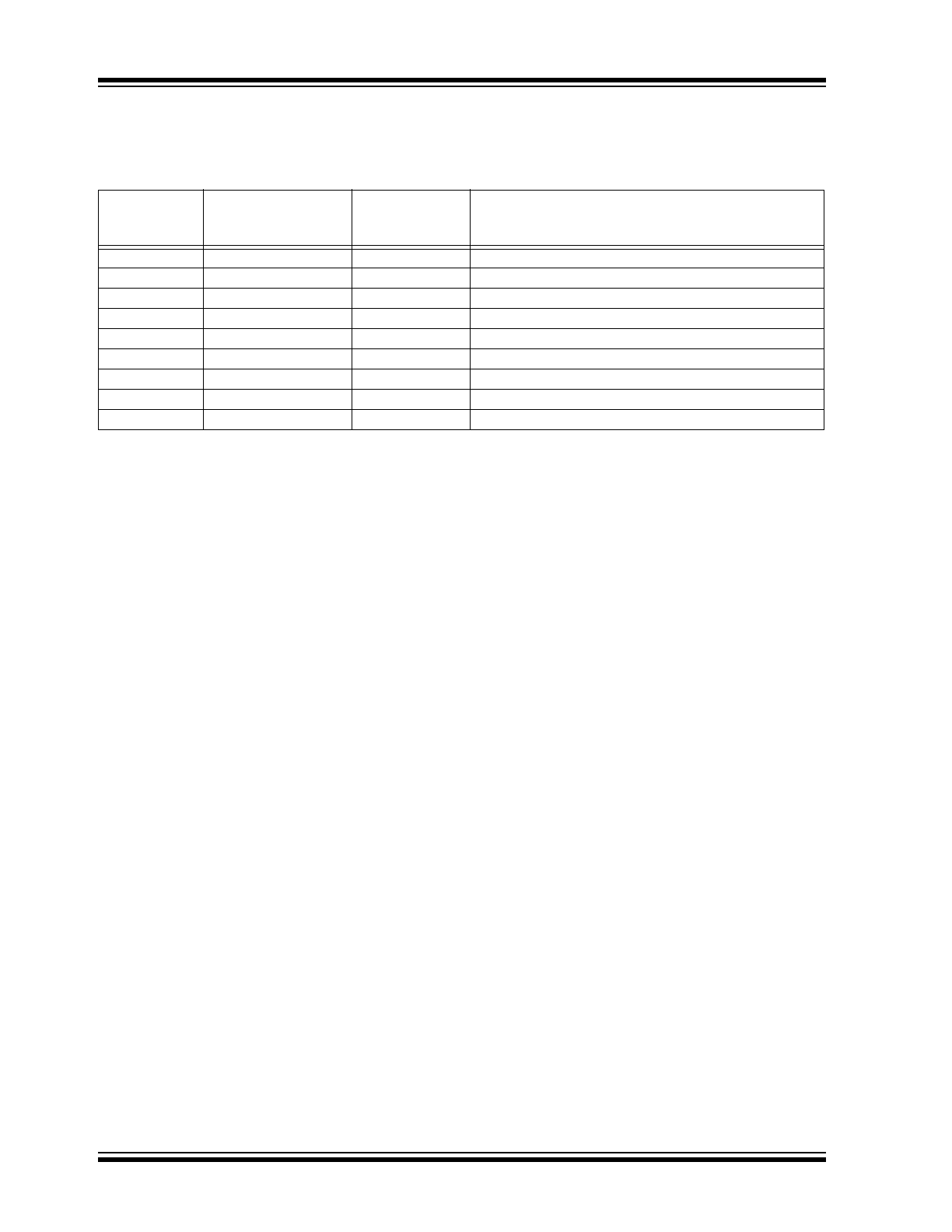
PIN DESCRIPTIONS
The descriptions of the pins are listed in
Table 2-1
.
TABLE 2-1:
PIN FUNCTION TABLE
Pin No.
(8-Pin PDIP,
CERDIP)
Pin No.
(16-Pin SOIC Wide)
Symbol
Description
1
1
C1-
See Section 3.1 “Booster Function” for description
2
3
C1+
See Section 3.1 “Booster Function” for description
3
5
C2
See Section 3.1 “Booster Function” for description
4
8
GND
Ground.
5
9
OUT
Output
6
11
V
BOOST
See Section 3.1 “Booster Function” for description
7
13
IN
Control Input
8
16
V
DD
Supply Input
—
2, 4, 6, 7, 10, 12, 14, 15
NC
Not connected.
2001-2014 Microchip Technology Inc.
DS20001426D-page 5
TC4626/TC4627
3.0
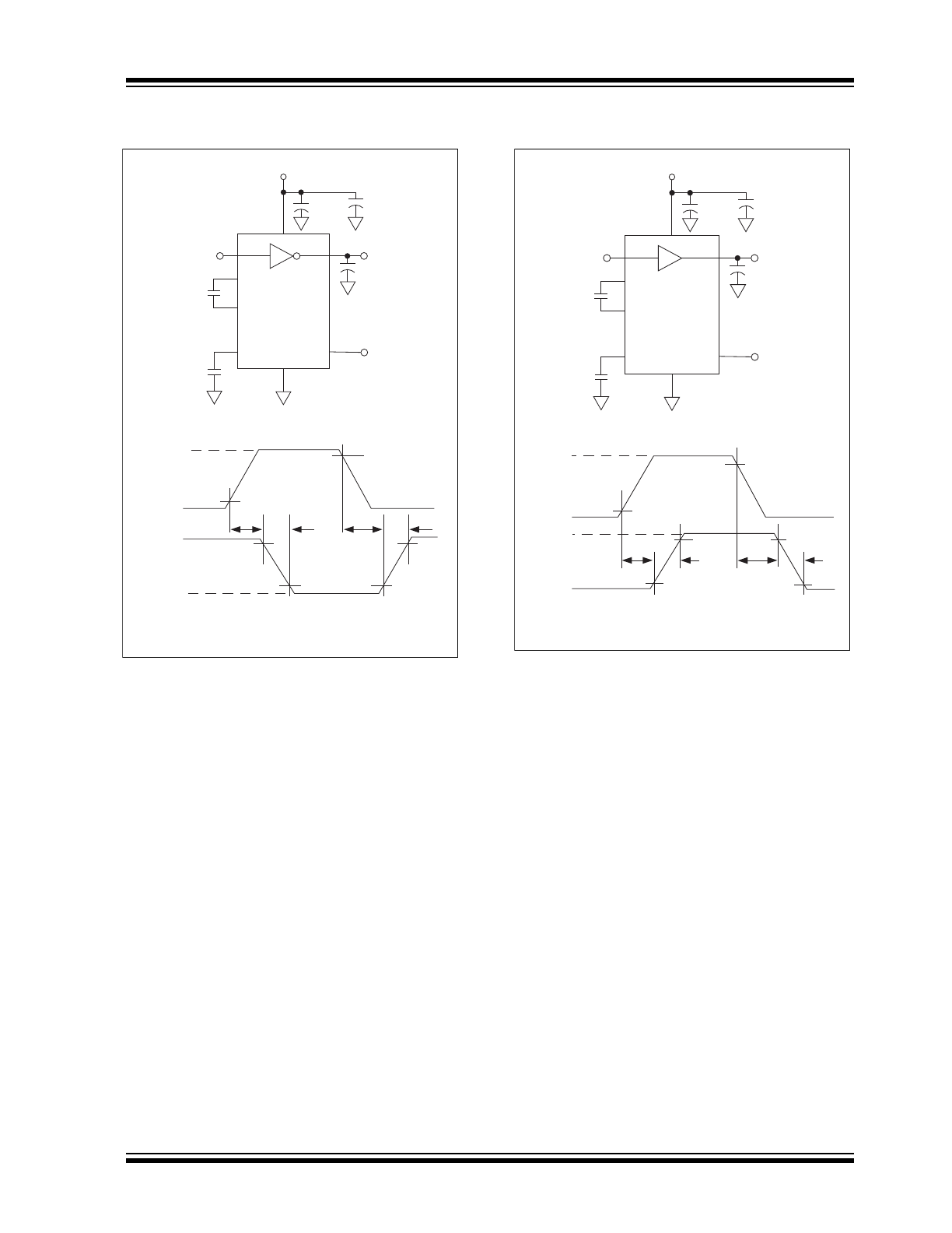
APPLICATIONS INFORMATION
FIGURE 3-1:
Inverting Driver Switching
Time.
FIGURE 3-2:
Noninverting Driver
Switching Time.
0.1
ȝF Ceramic
V
BOOST
+5V
10%
90%
10%
90%
10%
90%
0V
0V
TC4626
C1+
C1-
V
DD
= 5V
C
2
V
BOOST
3
8
7
1
6
5
2
4
C
L
= 1000
pF
Input
Input
Output
t
D1
t
F
t
D2
Input: 100kHz,
square wave,
t
RISE
= t
FALL
≤ 10ns
Output
t
R
C
1
10
ȝF
C
2
10
ȝF
C
3
10
ȝF
0.1
ȝF Ceramic
V
BOOST
+5V
TC4627
C1+
C1-
V
DD
= 5V
C
2
V
BOOST
3
8
7
1
6
5
2
4
C
L
= 1000
pF
Input
Input
Output
t
D1
t
F
t
D2
Input: 100kHz,
square wave,
t
RISE
= t
FALL
≤ 10ns
Output
t
R
C
1
10
ȝF
C
2
10
ȝF
C
3
10
ȝF
90%
10%
10%
10%
90%
0V
0V
90%
TC4626/TC4627
DS20001426D-page 6
2001-2014 Microchip Technology Inc.
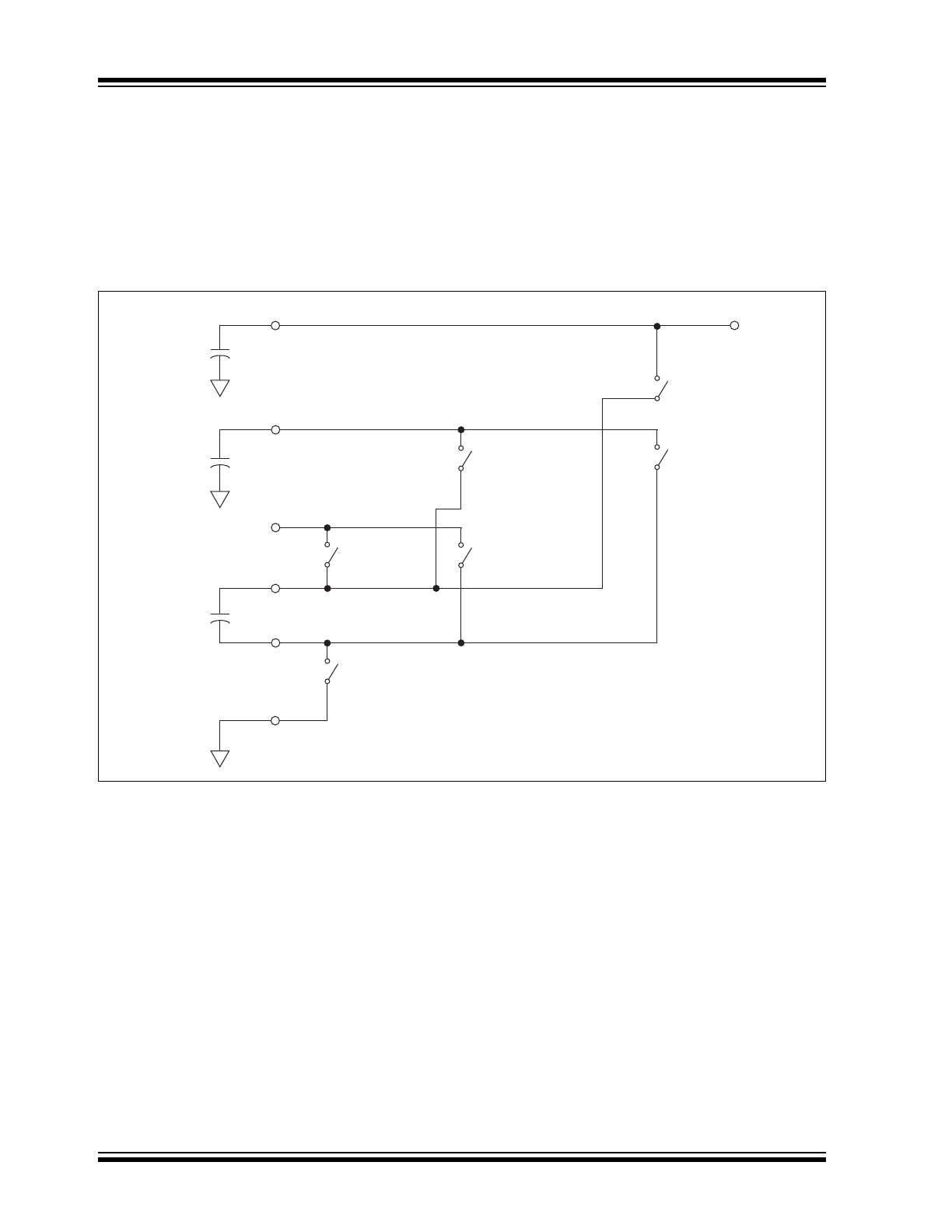
3.1
BOOSTER FUNCTION
The voltage booster is an unregulated voltage tripler
circuit. The tripler consists of three sets of internal
switches and three external capacitors. S1a and S1b
charge capacitor C1 to V
DD
potential. S2a and S2b add
C1 potential to V
DD
input to charge C2 to 2 x V
DD
. S3a
and S3b add C1 potential to C2 to charge C3 to 3 x
V
DD
. The position of the switches is controlled by the
internal four-phase clock.
FIGURE 3-3:
Voltage Booster.
C
3
C
2
6
3
8
2
C
1
S1a
S1b
GND
4
S2a
S2b
2 x V
DD
3 x V
DD
, V
BOOST
6
S3b
S3a
1
(4 to 6V)
V
DD
+
+
+
2001-2014 Microchip Technology Inc.
DS20001426D-page 7
TC4626/TC4627
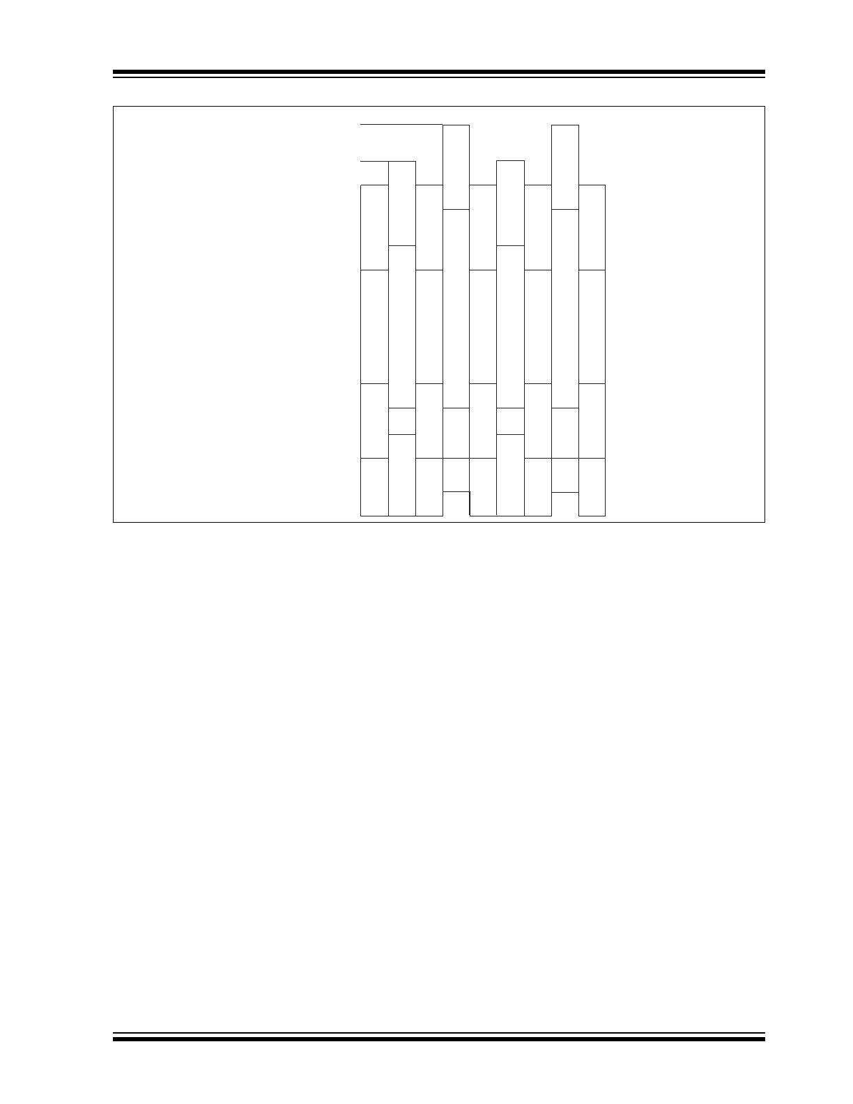
FIGURE 3-4:
Position of Switches.
Pin 2
Voltage
Pin 1
Voltage
3 x V
DD
2 x V
DD
V
DD
2 x V
DD
V
DD
0
On
Off
S1
On
Off
S2
On
Off
S3
Pin 1
CPF 2 Waveforms
TC4626/TC4627
DS20001426D-page 8
2001-2014 Microchip Technology Inc.
4.0
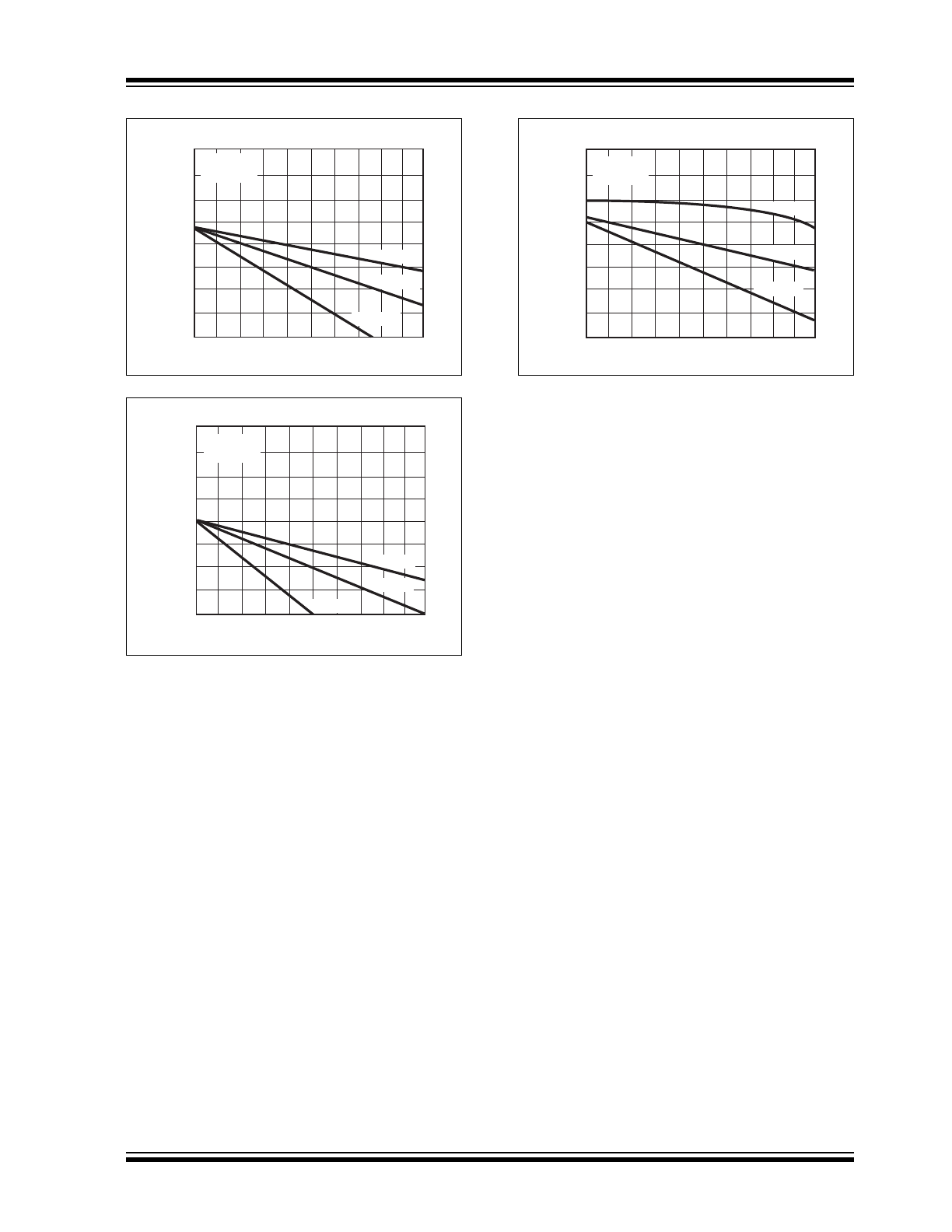
TYPICAL CHARACTERISTICS
Note:
The graphs and tables provided following this note are a statistical summary based on a limited number of
samples and are provided for informational purposes only. The performance characteristics listed herein
are not tested or guaranteed. In some graphs or tables, the data presented may be outside the specified
operating range (e.g., outside specified power supply range) and therefore outside the warranted range.
V
OUT
HI (Volts)
TC4626 V
OH
vs. Frequency
5
500 1,000 1,500 2,000 2,500
3,000 3,500
16
14
12
10
8
6
4
2
0
FREQUENCY (kHz)
470
2200
1000
V
S
= 5V
T
A
= -55°C
FREQUENCY (kHz)
TC4626 V
OH
vs. Frequency
5
500 1,000 1,500 2,000 2,500
3,000 3,500
14
12
10
8
6
4
2
0
470
2200
1000
V
OUT
HI (Volts)
V
S
= 5V
T
A
= 125°C
Time (nsec)
-40
-20
0
20
40
60
80
60
50
40
30
20
0
100
10
120
Delay Time vs. Temperature
V
S
= 5V
C
LOAD
= 1000
Input = 0-5V;
T
R
& T
F
<10
@ <20kHz
TEMPERATURE (
°C)
t
D2
t
D1
t
RISE
t
FALL
V
OUT
HI (Volts)
14
12
10
8
6
4
2
0
10
500 1,000 1,500 2,000 2,500
3,000 3,500
FREQUENCY (kHz)
470
2200
1000
V
S
= 5V
T
A
= 25°C
TC4626 V
OH
vs. Frequency
Time (nsec)
-40 -20
0
20
40
60
80
100
80
60
40
20
0
Delay Time vs. Temperature
100
120
Input = 0-5V;
T
R
& T
F
<10
@ <20
V
S
= 4V
C
LOAD
= 1000
TEMPERATURE (
°C)
t
D2
t
D1
t
RISE
t
FALL
Time (nsec)
-40
-20
0
20
40
60
80
50
40
30
20
0
100
10
120
Delay Time vs. Temperature
V
S
= 6V
C
LOAD
= 1000
Input = 0-5V;
T
R
& T
F
<10
@ <20kHz
TEMPERATURE (
°C)
t
D2
t
D1
t
RISE
t
FALL
2001-2014 Microchip Technology Inc.
DS20001426D-page 9
TC4626/TC4627
V
OUT
HI (Volts)
1
2
3
4
5
6
7
13
12
11
10
9
8
8
FREQUENCY x 100 kHz
9
10
0
14
15
16
2,200
470
1,000
TC4626 V
OH
vs. Frequency
V
S
= 5V
T
A
= 25°C
V
OUT
HI (Volts)
1
2
3
4
5
6
7
13
12
11
10
9
8
8
FREQUENCY x 100 kHz
9
10
0
14
15
16
470
2,200
1,000
V
S
= 5V
T
A
= 125°C
TC4626 V
OH
vs. Frequency
1
2
3
4
5
6
7
13
12
11
10
9
8
8
FREQUENCY x 100 kHz
9
10
0
14
15
16
2,200
470
1,000
V
S
= 5V
T
A
= -55°C
TC4626 V
OH
vs. Frequency
V
OUT
HI (Volts)
TC4626/TC4627
DS20001426D-page 10
2001-2014 Microchip Technology Inc.
5.0
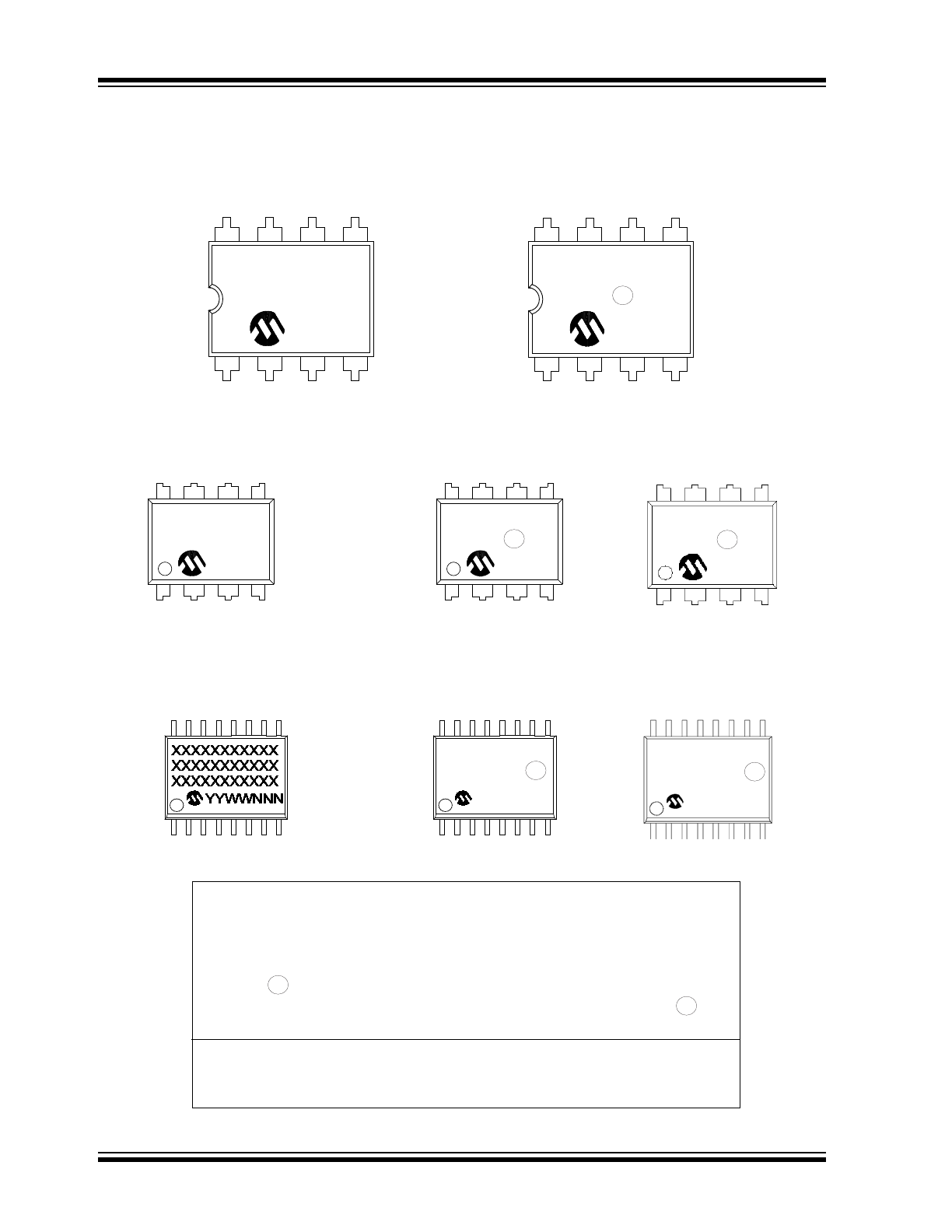
PACKAGING INFORMATION
5.1
Package Marking Information
8-Lead CERDIP (.300”) (TC4627 Only) Example
XXXXXNNN
XXXXXXXX
YYWW
8-Lead PDIP (300 mil)
Example
XXXXXXXX
XXXXXNNN
YYWW
16-Lead SOIC (7.50 mm)
Example
Legend:
XX...X
Customer-specific information
Y
Year code (last digit of calendar year)
YY
Year code (last 2 digits of calendar year)
WW
Week code (week of January 1 is week ‘01’)
NNN
Alphanumeric traceability code
Pb-free JEDEC
®
designator for Matte Tin (Sn)
*
This package is Pb-free. The Pb-free JEDEC designator ( )
can be found on the outer packaging for this package.
Note
:
In the event the full Microchip part number cannot be marked on one line, it will
be carried over to the next line, thus limiting the number of available
characters for customer-specific information.
3
e
3
e
TC4627
MJA ^^256
1423
3
e
TC4626
CPA ^^256
1423
TC4626
EPA ^^256
1423
3
e
3
e
OR
TC4627EOE
^^
1423256
3
e
TC4627COE
^^
1423256
3
e
OR