
2002-2013 Microchip Technology Inc.
DS20001420F-page 1
TC4421/TC4422
Features:
• High Peak Output Current: 9A
• Wide Input Supply Voltage Operating Range:
- 4.5V to 18V
• High Continuous Output Current: 2A Maximum
• Fast Rise and Fall Times:
- 30 ns with 4,700 pF Load
- 180 ns with 47,000 pF Load
• Short Propagation Delays: 30 ns (Typical)
• Low Supply Current:
- With Logic ‘1’ Input – 200 µA (Typical)
- With Logic ‘0’ Input – 55 µA (Typical)
• Low Output Impedance: 1.4
(Typical)
• Latch-Up Protected: Will Withstand 1.5A Output
Reverse Current
• Input Will Withstand Negative Inputs up to 5V
• Pin-Compatible with the TC4420/TC4429
6A MOSFET Driver
• Space-saving 8-Pin 6x5 DFN-S Package
Applications:
• Line Drivers for Extra Heavily-Loaded Lines
• Pulse Generators
• Driving the Largest MOSFETs and IGBTs
• Local Power ON/OFF Switch
• Motor and Solenoid Driver
General Description:
TC4421/TC4422 are high-current buffers/drivers
capable of driving large MOSFETs and IGBTs.
These devices are essentially immune to any form of
upset, except direct overvoltage or over-dissipation.
They cannot be latched under any conditions within
their power and voltage ratings. These parts are not
subject to damage or improper operation when up to
5V of ground bounce is present on their ground
terminals. They can accept, without damage or logic
upset, more than 1A inductive current of either polarity
being forced back into their outputs. In addition, all
terminals are fully protected against up to 4 kV of
electrostatic discharge.
The TC4421/TC4422 inputs may be driven directly
from either TTL or CMOS (3V to 18V). In addition,
300 mV of hysteresis is built into the input, providing
noise immunity and allowing the device to be driven
from slowly rising or falling waveforms.
With both surface-mount and pin-through-hole
packages and four operating temperature range
offerings, the TC4421/TC4422 family of 9A MOSFET
drivers fits into any application where high gate/line
capacitance drive is required.
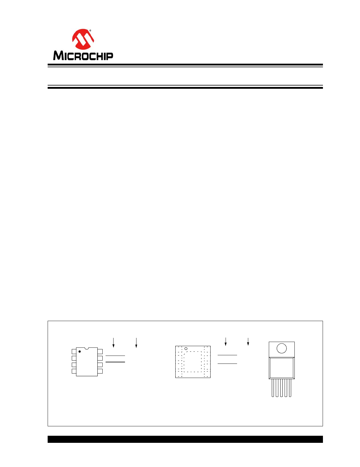
Package Types
(
1
)
V
DD
5
6
7
8
OUTPUT
GND
OUTPUT
TC4421
8-Pin PDIP/
1
2
3
4
V
DD
INPUT
NC
GND
5-Pin TO-220
V
DD
GND
INP
U
T
GND
OUTP
UT
TC4421
TC4422
Tab is
Common
to V
DD
Note 1: Duplicate pins must both be connected for proper operation.
2: Includes electrically isolated Exposed Thermal Pad (EP), see
Table 3-1
.
TC4422
V
DD
OUTPUT
GND
OUTPUT
SOIJ
8-Pin 6x5 DFN-S
(
2
)
V
DD
INPUT
NC
GND
V
DD
OUTPUT
GND
OUTPUT
TC4421 TC4422
V
DD
OUTPUT
GND
OUTPUT
1
2
3
4
8
7
6
5
EP
9
9A High-Speed MOSFET Drivers
TC4421/TC4422
DS20001420F-page 2
2002-2013 Microchip Technology Inc.
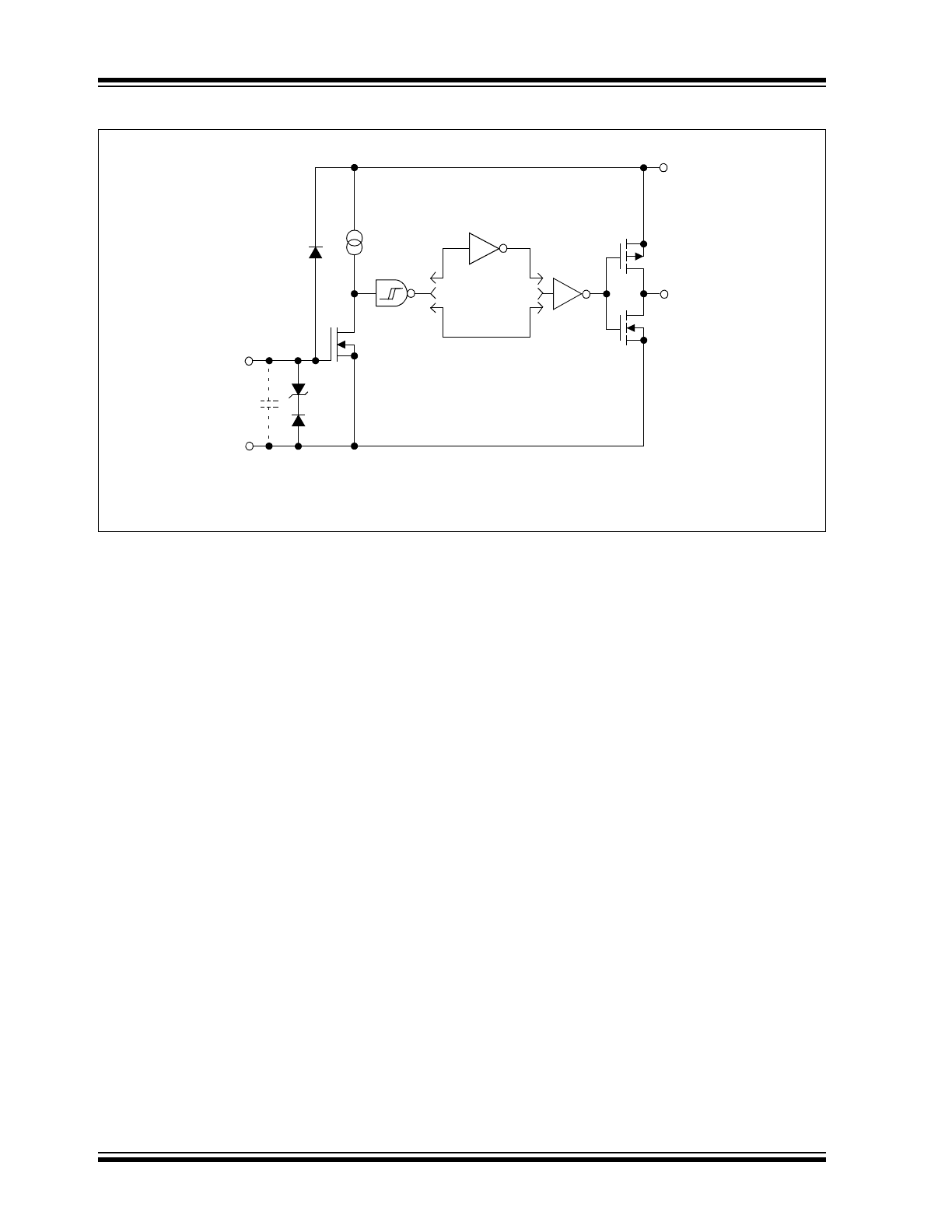
Functional Block Diagram
Effective
Input
Output
Input
GND
V
DD
300 mV
4.7V
C = 25 pF
Inverting
Non-Inverting
200 µA
TC4421
TC4422
2002-2013 Microchip Technology Inc.
DS20001420F-page 3
TC4421/TC4422
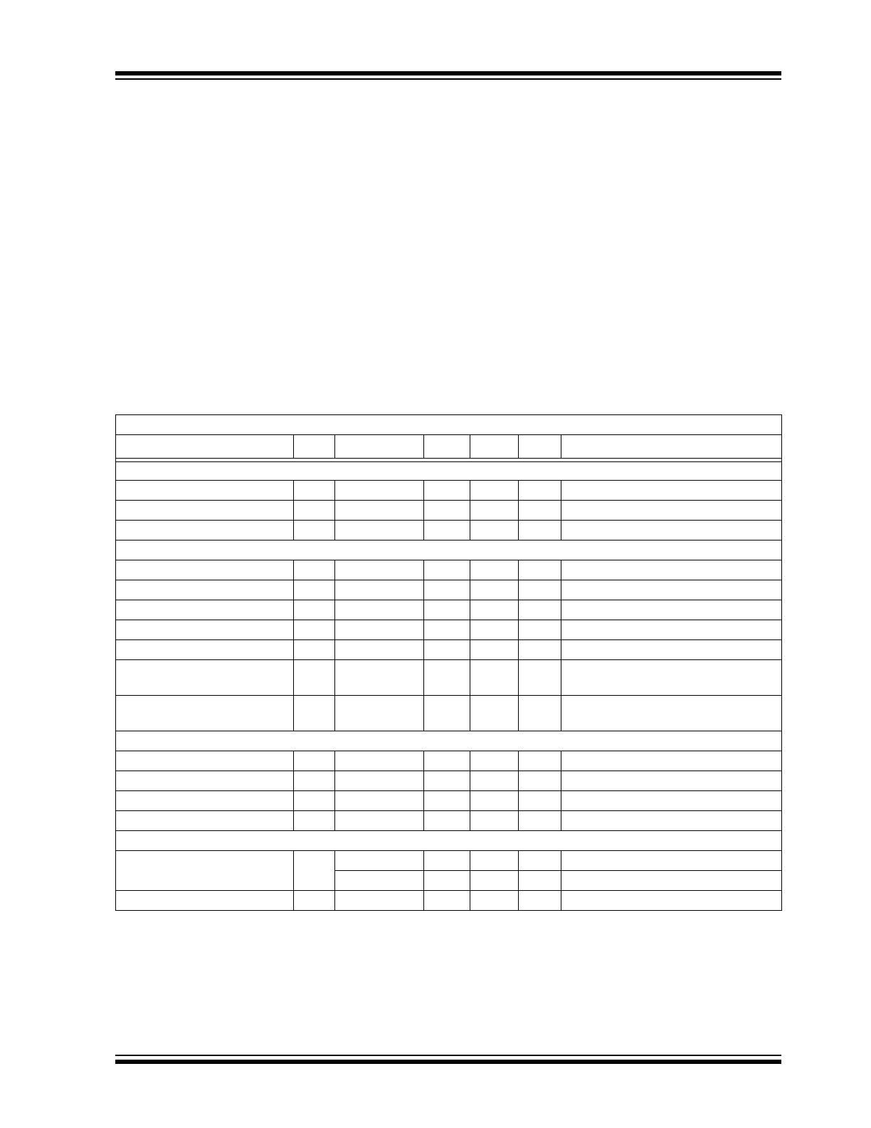
1.0
ELECTRICAL
CHARACTERISTICS
Absolute Maximum Ratings†
Supply Voltage ..................................................... +20V
Input Voltage .................... (V
DD
+ 0.3V) to (GND – 5V)
Input Current (V
IN
> V
DD
)................................... 50 mA
Package Power Dissipation (T
A
70°C)
5-Pin TO-220 .................................................... 1.6W
DFN-S ..........................................................
Note 2
PDIP ............................................................ 730 mW
SOIJ ............................................................ 750 mW
Package Power Dissipation (T
A
25°C)
5-Pin TO-220 (with heatsink) .......................... 12.5W
Thermal Impedances (to case)
5-Pin TO-220 R
J-C
...................................... 10°C/W
† Notice: Stresses above those listed under “Absolute
Maximum Ratings” may cause permanent damage to
the device. These are stress ratings only and functional
operation of the device at these or any other conditions
above those indicated in the operation sections of the
specifications is not implied. Exposure to Absolute
Maximum Rating conditions for extended periods may
affect device reliability.
DC CHARACTERISTICS
Electrical Specifications: Unless otherwise noted, T
A
= +25°C with 4.5V
V
DD
18V.
Parameters
Sym
Min
Typ
Max
Units
Conditions
Input
Logic ‘1’, High-Input Voltage
V
IH
2.4
1.8
—
V
Logic ‘0’, Low-Input Voltage
V
IL
—
1.3
0.8
V
Input Current
I
IN
–10
—
+10
µA
0V
V
IN
V
DD
Output
High-Output Voltage
V
OH
V
DD
– 0.025
—
—
V
DC test
Low-Output Voltage
V
OL
—
—
0.025
V
DC test
Output Resistance, High
R
OH
—
1.4
—
I
OUT
= 10 mA, V
DD
= 18V
Output Resistance, Low
R
OL
—
0.9
1.7
I
OUT
= 10 mA, V
DD
= 18V
Peak Output Current
I
PK
—
9.0
—
A
V
DD
= 18V
Continuous Output Current
I
DC
2
—
—
A
10V
V
DD
18V, T
A
= +25°C
(TC4421/TC4422 CAT only) (
Note 3
)
Latch-Up Protection
Withstand Reverse Current
I
REV
—
> 1.5
—
A
Duty cycle
2%, t 300 µsec
Switching Time (
Note 1
)
Rise Time
t
R
—
60
75
ns
Figure 4-1
, C
L
= 10,000 pF
Fall Time
t
F
—
60
75
ns
Figure 4-1
, C
L
= 10,000 pF
Delay Time
t
D1
—
30
60
ns
Figure 4-1
Delay Time
t
D2
—
33
60
ns
Figure 4-1
Power Supply
Power Supply Current
I
S
—
0.2
1.5
mA
V
IN
= 3V
—
55
150
µA
V
IN
= 0V
Operating Input Voltage
V
DD
4.5
—
18
V
Note 1:
Switching times ensured by design.
2:
Package power dissipation is dependent on the copper pad area on the PCB.
3:
Tested during characterization, not production tested.
TC4421/TC4422
DS20001420F-page 4
2002-2013 Microchip Technology Inc.
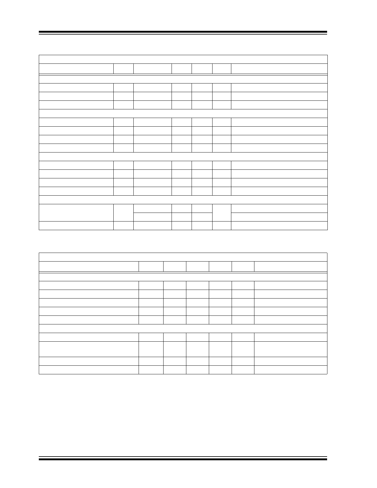
DC CHARACTERISTICS (OVER OPERATING TEMPERATURE RANGE)
Electrical Specifications: Unless otherwise noted, over the operating temperature range with 4.5V
V
DD
18V.
Parameters
Sym
Min
Typ
Max
Units
Conditions
Input
Logic ‘1’, High-Input Voltage
V
IH
2.4
—
—
V
Logic ‘0’, Low-Input Voltage
V
IL
—
—
0.8
V
Input Current
I
IN
–10
—
+10
µA
0V
V
IN
V
DD
Output
High-Output Voltage
V
OH
V
DD
– 0.025
—
—
V
DC TEST
Low-Output Voltage
V
OL
—
—
0.025
V
DC TEST
Output Resistance, High
R
OH
—
2.4
3.6
I
OUT
= 10 mA, V
DD
= 18V
Output Resistance, Low
R
OL
—
1.8
2.7
I
OUT
= 10 mA, V
DD
= 18V
Switching Time (
Note 1
)
Rise Time
t
R
—
60
120
ns
Figure 4-1
, C
L
= 10,000 pF
Fall Time
t
F
—
60
120
ns
Figure 4-1
, C
L
= 10,000 pF
Delay Time
t
D1
—
50
80
ns
Figure 4-1
Delay Time
t
D2
—
65
80
ns
Figure 4-1
Power Supply
Power Supply Current
I
S
—
—
3
mA
V
IN
= 3V
—
—
0.2
V
IN
= 0V
Operating Input Voltage
V
DD
4.5
—
18
V
Note 1:
Switching times ensured by design.
TEMPERATURE CHARACTERISTICS
Electrical Specifications: Unless otherwise noted, all parameters apply with 4.5V
V
DD
18V.
Parameters
Sym
Min
Typ
Max
Units
Conditions
Temperature Ranges
Specified Temperature Range (C)
T
A
0
—
+70
°C
Specified Temperature Range (E)
T
A
–40
—
+85
°C
Specified Temperature Range (V)
T
A
–40
—
+125
°C
Maximum Junction Temperature
T
J
—
—
+150
°C
Storage Temperature Range
T
A
–65
—
+150
°C
Package Thermal Resistances
Thermal Resistance, 5L-TO-220
JA
—
39.5
—
°C/W
Thermal Resistance, 8L-6x5 DFN-S
JA
—
35.7
—
°C/W
Typical 4-layer board with
vias to ground plane
Thermal Resistance, 8L-PDIP
JA
—
89.3
—
°C/W
Thermal Resistance, 8L-SOIJ
JA
—
117
—
°C/W
2002-2013 Microchip Technology Inc.
DS20001420F-page 5
TC4421/TC4422
2.0
TYPICAL PERFORMANCE CURVES
Note: Unless otherwise indicated, T
A
= +25°C with 4.5V
V
DD
18V.
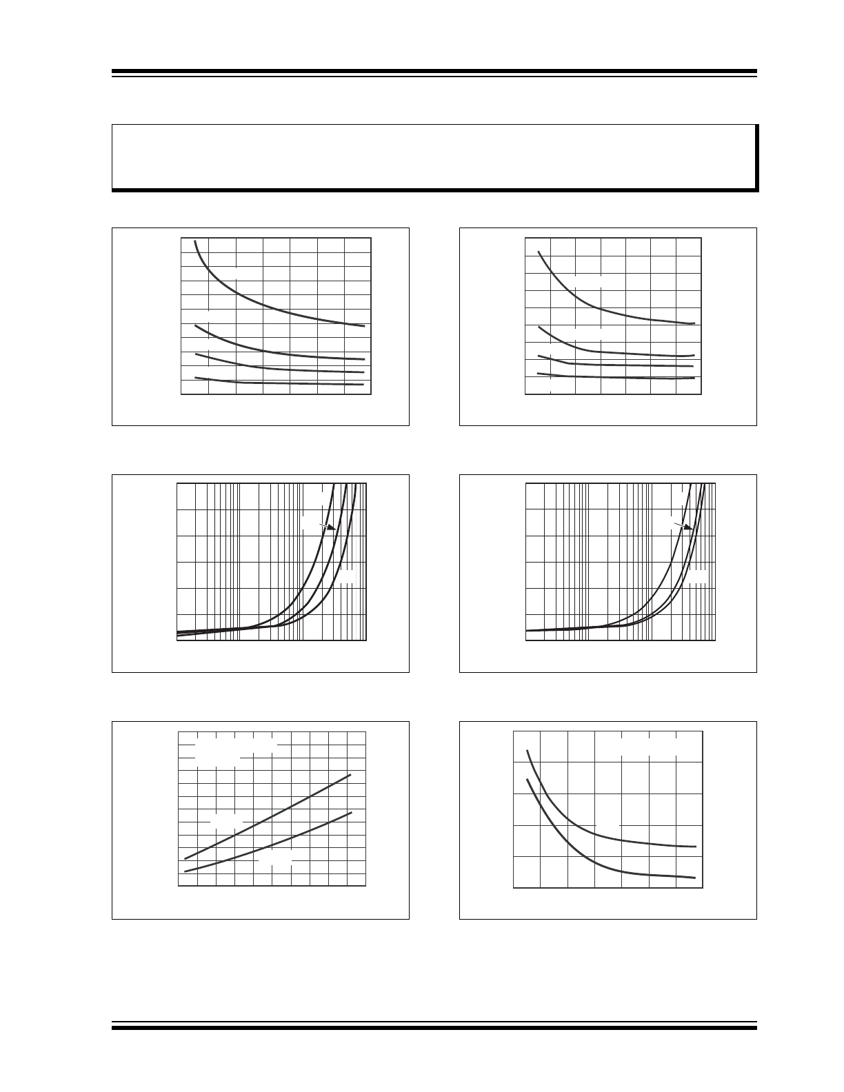
FIGURE 2-1:
Rise Time vs. Supply
Voltage.
FIGURE 2-2:
Rise Time vs. Capacitive
Load.
FIGURE 2-3:
Rise and Fall Times vs.
Temperature.
FIGURE 2-4:
Fall Time vs. Supply
Voltage.
FIGURE 2-5:
Fall Time vs. Capacitive
Load.
FIGURE 2-6:
Propagation Delay vs.
Supply Voltage.
Note:
The graphs and tables provided following this note are a statistical summary based on a limited number of
samples and are provided for informational purposes only. The performance characteristics listed herein
are not tested or guaranteed. In some graphs or tables, the data presented may be outside the specified
operating range (e.g., outside specified power supply range) and therefore outside the warranted range.
220
200
180
160
140
120
100
80
60
40
20
0
4
6
8
10
12
14
16
18
1000 pF
4700 pF
10,000 pF
22,000 pF
t
RISE
(nsec)
V
DD
(V)
t
RISE
(nsec)
5V
15V
300
250
200
150
100
50
0
100
1000
10,000
100,000
10V
C
LOAD
(pF)
90
60
40
30
70
50
80
-40
0
40
80
120
Time (nsec)
T
A
(
°
C)
C
LOAD
= 10,000 pF
V
DD
= 15V
t
FALL
t
RISE
180
160
140
120
100
80
60
40
20
0
4
6
8
10
12
14
16
18
1000 pF
4700 pF
10,000 pF
22,000 pF
t
FALL
(nsec)
V
DD
(V)
t
FALL
(nsec)
300
250
200
150
100
50
0
100
1000
10,000
5V
10V
15V
100,000
C
LOAD
(pF)
50
8
10
12
14
16
18
4
Time (nsec)
45
40
35
30
25
6
V
DD
(V)
C
LOAD
= 1000 pF
t
D1
t
D2
TC4421/TC4422
DS20001420F-page 6
2002-2013 Microchip Technology Inc.
Note: Unless otherwise indicated, T
A
= +25°C with 4.5V
V
DD
18V.
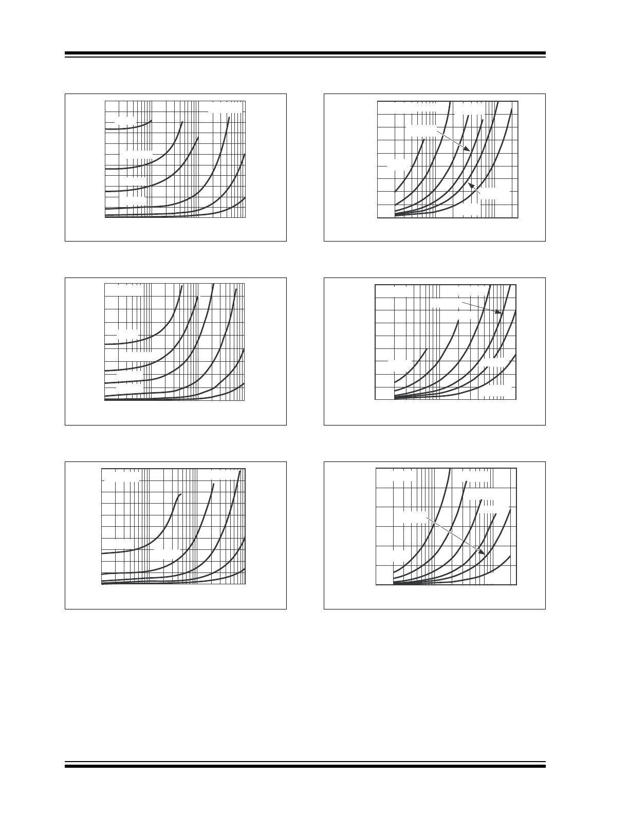
FIGURE 2-7:
Supply Current vs.
Capacitive Load (V
DD
= 18V).
FIGURE 2-8:
Supply Current vs.
Capacitive Load (V
DD
= 12V).
FIGURE 2-9:
Supply Current vs.
Capacitive Load (V
DD
= 6V).
FIGURE 2-10:
Supply Current vs.
Frequency (V
DD
= 18V).
FIGURE 2-11:
Supply Current vs.
Frequency (V
DD
= 12V).
FIGURE 2-12:
Supply Current vs.
Frequency (V
DD
= 6V).
220
100
200
180
160
140
120
100
80
60
40
20
0
100,000
10,000
1000
1.125 MHz
632 kHz
200 kHz
20 kHz
2 MHz
63.2 kHz
I
SUPPLY
(mA)
C
LOAD
(pF)
V
DD
= 18V
I
SUPPLY
(mA)
180
160
140
120
100
60
0
80
40
20
1.125 MHz
63.2 kHz
20 kHz
632 kHz
200 kHz
2 MHz
100
100,000
10,000
1000
V
DD
= 12V
C
LOAD
(pF)
I
SUPPLY
(mA)
100
90
80
70
60
50
40
30
20
10
0
20 kHz
632 kHz
200 kHz
2 MHz
63.2 kHz
100
100,000
10,000
1000
V
DD
= 6V
C
LOAD
(pF)
Frequency (kHz)
180
100
80
60
40
20
0
120
140
160
22,000 pF
470 pF
10,000 pF
0.1 µF
4700 pF
10
100
1000
47,000 pF
I
SUPPLY
(mA)
V
DD
= 18V
I
SUPPLY
(mA)
Frequency (kHz)
180
100
80
60
40
20
0
120
140
160
470 pF
22,000 pF
4700 pF
10,000 pF
47,000 pF
10
100
1000
V
DD
= 12V
0.1 µF
I
SUPPLY
(mA)
47,000 pF
120
40
20
0
100
4700 pF
10
Frequency (kHz)
100
1000
60
80
22,000 pF
470 pF
10,000 pF
10
100
1000
V
DD
= 6V
0.1 µF
2002-2013 Microchip Technology Inc.
DS20001420F-page 7
TC4421/TC4422
Note: Unless otherwise indicated, T
A
= +25°C with 4.5V
V
DD
18V.
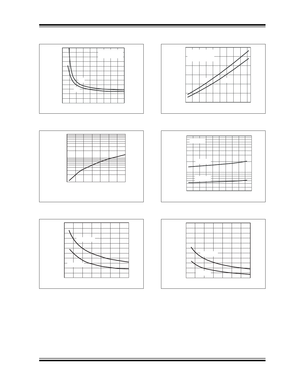
FIGURE 2-13:
Propagation Delay vs. Input
Amplitude.
FIGURE 2-14:
Crossover Energy vs.
Supply Voltage.
FIGURE 2-15:
High-State Output
Resistance vs. Supply Voltage.
FIGURE 2-16:
Propagation Delay vs.
Temperature.
FIGURE 2-17:
Quiescent Supply Current
vs. Temperature.
FIGURE 2-18:
Low-State Output
Resistance vs. Supply Voltage.
120
Time (nsec)
110
100
90
80
70
60
50
40
30
20
10
0
1
2
3
4
5
6
7
8
9
10
Input Amplitude (V)
V
DD
= 10V
C
LOAD
= 10,000 pF
t
D1
t
D2
10-7
10-6
A•sec
NOTE:
The values on this graph represent the loss seen
by the driver during a complete cycle. For the loss
in a single transition, divide the stated value by 2.
4
6
8
10
12
14
16
18
V
DD
(V)
10-8
6
4
6
8
10
12
14
16
18
5.5
5
4.5
4
3.5
3
2.5
2
1.5
1
0.5
V
DD
(V)
T
J
= 150°C
T
J
= 25°C
R
DS(ON)
(
Ω
)
50
–40 –20
0
20
40
60
80
100 120
–60
Time (nsec)
45
40
35
30
25
20
T
A
(
°
C)
t
D1
t
D2
V
DD
= 18V
C
LOAD
= 10,000 pF
V
IN
= 5V
10
2
-40 -20
0
20
40
60
80 100 120
-60
V
DD
= 18V
Input = 1
Input = 0
I
QUIESCENT
(µ
A)
T
J
(°C)
10
3
R
DS(ON)
(
Ω
)
4
6
8
10
12
14
16
18
6
5.5
5
4.5
4
3.5
3
2.5
2
1.5
1
0.5
V
DD
(V)
T
J
= 150°C
T
J
= 25°C
TC4421/TC4422
DS20001420F-page 8
2002-2013 Microchip Technology Inc.
3.0
PIN DESCRIPTIONS
The descriptions of the pins are listed in
Table 3-1
.
3.1
Supply Input (V
DD
)
The V
DD
input is the bias supply for the MOSFET driver
and is rated for 4.5V to 18V with respect to the ground
pin. The V
DD
input should be bypassed to ground with
a local ceramic capacitor. The value of the capacitor
should be chosen based on the capacitive load that is
being driven. A minimum value of 1.0 µF is suggested.
3.2
Control Input (INPUT)
The MOSFET driver input is a high-impedance,
TTL/CMOS compatible input. The input also has
300 mV of hysteresis between the high and low
thresholds that prevents output glitching even when the
rise and fall time of the input signal is very slow.
3.3
CMOS Push-Pull Output (OUTPUT,
OUTPUT)
The MOSFET driver output is a low-impedance,
CMOS, push-pull style output capable of driving a
capacitive load with 9.0A peak currents. The MOSFET
driver output is capable of withstanding 1.5A peak
reverse currents of either polarity.
3.4
Ground (GND)
The ground pins are the return path for the bias current
and for the high peak currents that discharge the load
capacitor. The ground pins should be tied into a ground
plane or have very short traces to the bias supply
source return.
3.5
Exposed Thermal Pad (EP)
The exposed thermal pad of the 6x5 DFN-S package is
not internally connected to any potential. Therefore,
this pad can be connected to a ground plane or other
copper plane on a printed circuit board to aid in heat
removal from the package.
TABLE 3-1:
PIN FUNCTION TABLE
Pin No.
PDIP, SOIJ
Pin No.
6x5 DFN-S
Pin No.
TO-220
Symbol
Description
1
1
—
V
DD
Supply input, 4.5V to 18V
2
2
1
INPUT
Control input, TTL/CMOS compatible input
3
3
—
NC
No connection
4
4
2
GND
Ground
5
5
4
GND
Ground
6
6
5
OUTPUT/OUTPUT
CMOS push-pull output
7
7
—
OUTPUT/OUTPUT
CMOS push-pull output
8
8
3
V
DD
Supply input, 4.5V to 18V
—
9
—
EP
Exposed thermal pad
—
—
TAB
V
DD
Thermal tab is at the V
DD
potential
2002-2013 Microchip Technology Inc.
DS20001420F-page 9
TC4421/TC4422
4.0
APPLICATIONS INFORMATION
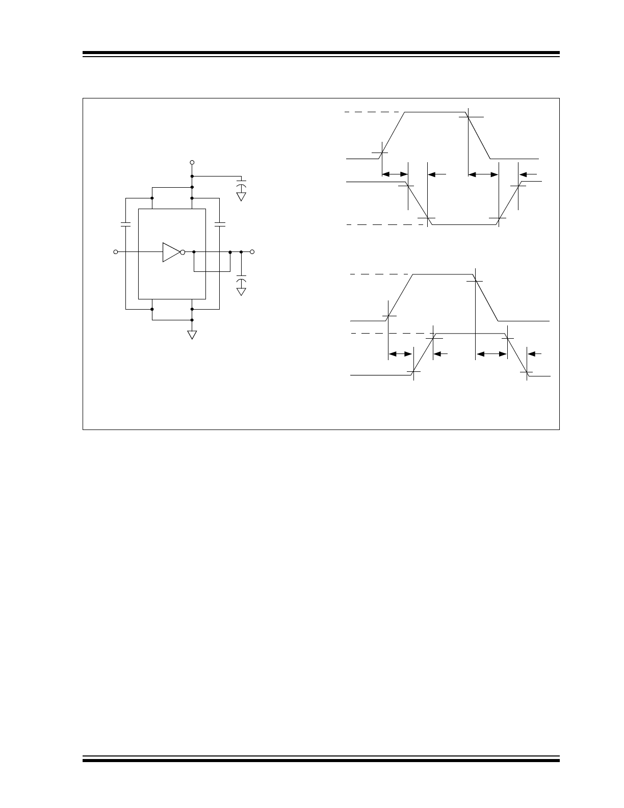
FIGURE 4-1:
Switching Time Test Circuits.
Inverting Driver
Non-Inverting Driver
Input
t
D1
t
F
t
R
t
D2
Input: 100 kHz,
square wave,
t
RISE
= t
FALL
10 nsec
Output
Input
Output
t
D1
t
F
t
R
t
D2
+5V
10%
90%
10%
90%
10%
90%
+18V
0V
90%
10%
10%
10%
90%
+5V
+18V
0V
0V
0V
90%
2
6
7
5
4
1
8
C
L
= 10,000 pF
0.1 µF
4.7 µF
Input
V
DD
= 18V
Output
0.1 µF
Note: Pinout shown is for the DFN-S, PDIP and SOIJ packages.
TC4421
TC4422
TC4421/TC4422
DS20001420F-page 10
2002-2013 Microchip Technology Inc.
5.0
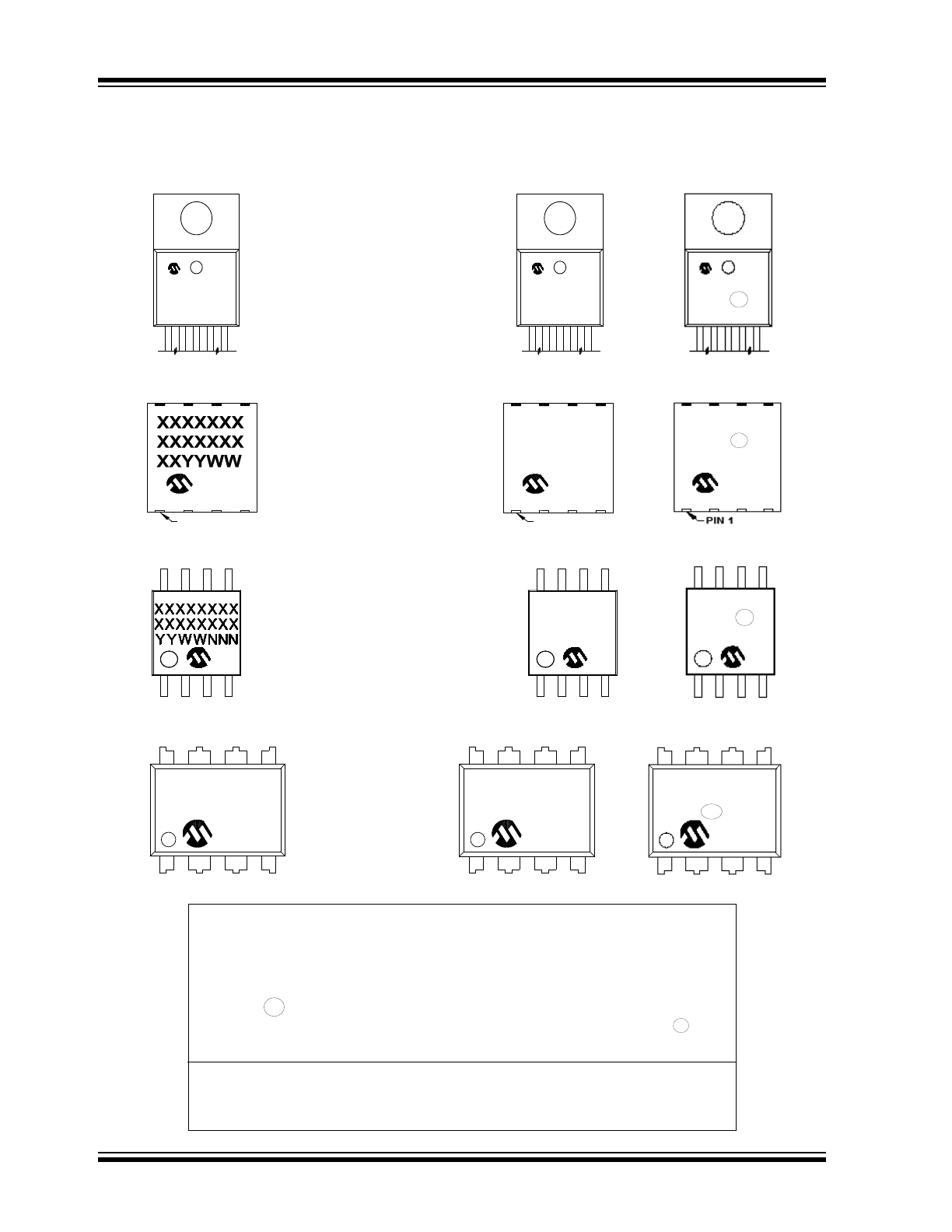
PACKAGING INFORMATION
5.1
Package Marking Information
YYWWNNN
XXXXXXXXX
XXXXXXXXX
Legend: XX...X
Customer-specific information
Y
Year code (last digit of calendar year)
YY
Year code (last 2 digits of calendar year)
WW
Week code (week of January 1 is week ‘01’)
NNN
Alphanumeric traceability code
Pb-free JEDEC designator for Matte Tin (Sn)
*
This package is Pb-free. The Pb-free JEDEC designator ( )
can be found on the outer packaging for this package.
Note:
In the event the full Microchip part number cannot be marked on one line, it will
be carried over to the next line, thus limiting the number of available
characters for customer-specific information.
3
e
3
e
5-Lead TO-220
Example
TC4421CAT
1318256
OR
8-Lead DFN-S (6x5x0.9 mm)
Example
PIN 1
NNN
PIN 1
TC4421
EMF
1318
256
OR
8-Lead PDIP (300 mil)
Example
XXXXXXXX
XXXXXNNN
YYWW
TC4421
CPA256
OR
8-Lead SOIJ (5.28 mm)
Example
TC4421
ESM
1318256
TC4421
ESM ^^
1318256
3
e
OR
TC4421
CPA^^ 256
1318
3
e
TC4421
CAT ^^
1318256
3
e
TC4421
EMF ^^
1318
256
3
e