
2005-2012 Microchip Technology Inc.
DS21933B-page 1
TC4420M/TC4429M
Features
• Latch-Up Protected: Will Withstand >1.5A
Reverse Output Current
• Logic Input: Will Withstand Negative Swing
Up To 5V
• ESD Protected: 4 kV
• Matched Rise and Fall Times:
- 25 ns (2500 pF load)
• High Peak Output Current: 6A
• Wide Input Supply Voltage Operating Range:
- 4.5V to 18V
• High Capacitive Load Drive Capability: 10,000 pF
• Short Delay Time: 55 ns (typical)
• CMOS/TTL-Compatible Input
• Low Supply Current With Logic ‘1’ Input:
- 450 µA (typical)
• Low Output Impedance: 2.5
• Output Voltage Swing to Within 25 mV of Ground
or V
DD
• Wide Operating Temperature Range:
- -55°C to +125°C
• See TC4420/TC4429 Data Sheet (DS21419) for
additional temperature range and package
offerings.
Applications
• Switch-mode Power Supplies
• Motor Controls
• Pulse Transformer Driver
• Class D Switching Amplifiers
General Description
The TC4420M/TC4429M are 6A (peak), single-output
MOSFET drivers. The TC4429M is an inverting driver
(pin-compatible with the TC429M), while the TC4420M
is a non-inverting driver. These drivers are fabricated in
CMOS for lower power and more efficient operation
versus bipolar drivers.
Both devices have TTL/CMOS-compatible inputs,
which can be driven as high as V
DD
+ 0.3V or as low as
-5V without upset or damage to the device. This elimi-
nates the need for external level-shifting circuitry and
its associated cost and size. The output swing is rail-to-
rail, ensuring better drive voltage margin, especially
during power-up/power-down sequencing. The propa-
gational delay time is only 55 ns (typical), while the out-
put rise and fall times are only 25 ns (typical) into
2500 pF across the usable power supply range.
Unlike other drivers, the TC4420M/TC4429M are virtu-
ally latch-up proof. They replace three or more discrete
components, saving PCB area and parts while
improving overall system reliability.
Package Types:
8-Pin CERDIP
1
2
3
4
V
DD
5
6
7
8
OUTPUT
GND
V
DD
INPUT
NC
GND
OUTPUT
TC4420M
Note: Duplicate pins must both be connected for
proper operation.
TC4429M
6A High-Speed MOSFET Drivers
1
2
3
4
5
6
7
8
V
DD
INPUT
NC
GND
V
DD
OUTPUT
GND
OUTPUT
TC4420M/TC4429M
DS21933B-page 2
2005-2012 Microchip Technology Inc.
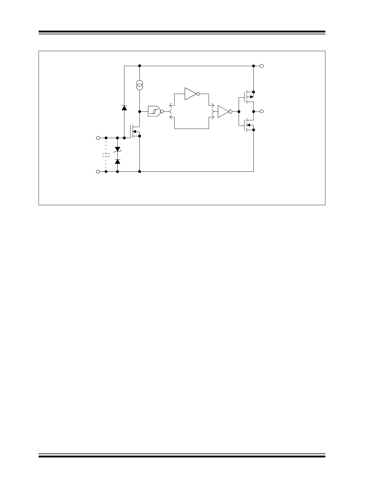
Functional Block Diagram
Effective
Input
Output
Input
GND
V
DD
300 mV
4.7V
C = 38 pF
500 µA
TC4429M
Inverting
TC4420M
Non-Inverting
2005-2012 Microchip Technology Inc.
DS21933B-page 3
TC4420M/TC4429M
1.0
ELECTRICAL
CHARACTERISTICS
Absolute Maximum Ratings†
Supply Voltage .....................................................+20V
Input Voltage ....................................-5V to V
DD
+ 0.3V
Input Current (V
IN
> V
DD
)................................... 50 mA
† Notice: Stresses above those listed under “Absolute
Maximum Ratings” may cause permanent damage to
the device. These are stress ratings only and functional
operation of the device at these or any other conditions
above those indicated in the operation sections of the
specifications is not implied. Exposure to Absolute
Maximum Rating conditions for extended periods may
affect device reliability.
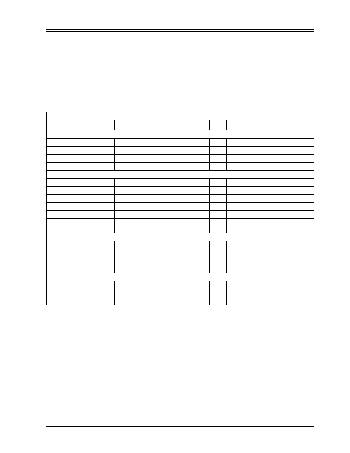
DC CHARACTERISTICS
Electrical Specifications: Unless otherwise noted, T
A
= +25°C with 4.5V
V
DD
18V.
Parameters
Sym
Min
Typ
Max
Units
Conditions
Input
Logic ‘1’, High Input Voltage
V
IH
2.4
1.8
—
V
Logic ‘0’, Low Input Voltage
V
IL
—
1.3
0.8
V
Input Voltage Range
V
IN
- 5
—
V
DD
+ 0.3
V
Input Current
I
IN
-10
—
+10
µA
0V
V
IN
V
DD
Output
High Output Voltage
V
OH
V
DD
– 0.025
—
—
V
DC TEST
Low Output Voltage
V
OL
—
—
0.025
V
DC TEST
Output Resistance, High
R
OH
—
2.1
2.8
I
OUT
= 10 mA, V
DD
= 18V
Output Resistance, Low
R
OL
—
1.5
2.5
I
OUT
= 10 mA, V
DD
= 18V
Peak Output Current
I
PK
—
6.0
—
A
V
DD
= 18V
Latch-Up Protection
Withstand Reverse Current
I
REV
—
> 1.5
—
A
Duty cycle
2%, t 300 µs
Switching Time (
Note 1
)
Rise Time
t
R
—
25
35
ns.
Figure 4-1
, C
L
= 2,500 pF
Fall Time
t
F
—
25
35
ns.
Figure 4-1
, C
L
= 2,500 pF
Delay Time
t
D1
—
55
75
ns.
Figure 4-1
Delay Time
t
D2
—
55
75
ns.
Figure 4-1
Power Supply
Power Supply Current
I
S
—
0.45
1.5
mA
V
IN
= 3V
—
55
150
µA
V
IN
= 0V
Operating Input Voltage
V
DD
4.5
—
18
V
Note 1:
Switching times ensured by design.
TC4420M/TC4429M
DS21933B-page 4
2005-2012 Microchip Technology Inc.
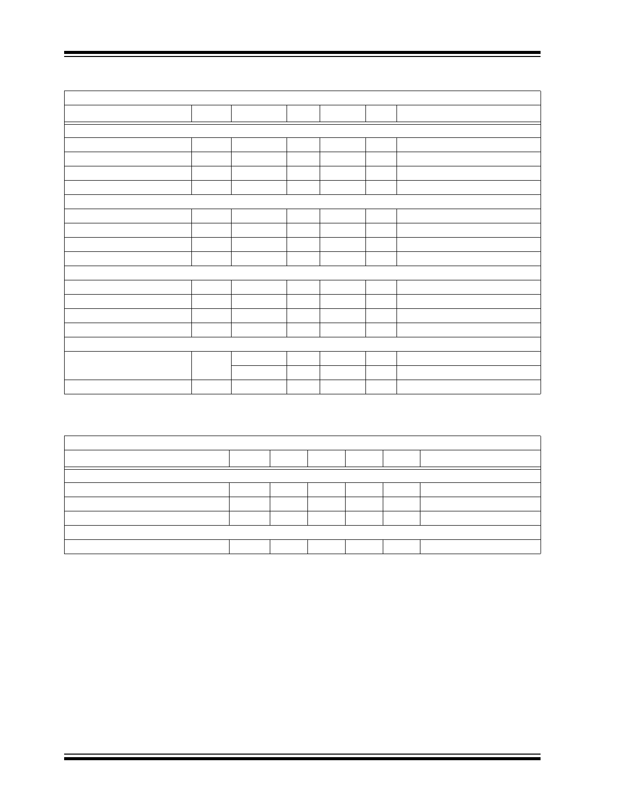
DC CHARACTERISTICS (OVER OPERATING TEMPERATURE RANGE)
Electrical Specifications: Unless otherwise noted, over operating temperature range with 4.5V
V
DD
18V.
Parameters
Sym
Min
Typ
Max
Units
Conditions
Input
Logic ‘1’, High Input Voltage
V
IH
2.4
—
—
V
Logic ‘0’, Low Input Voltage
V
IL
—
—
0.8
V
Input Voltage Range
V
IN
-5
—
V
DD
+ 0.3
V
Input Current
I
IN
-10
—
+10
µA
0V
V
IN
V
DD
Output
High Output Voltage
V
OH
V
DD
– 0.025
—
—
V
DC TEST
Low Output Voltage
V
OL
—
—
0.025
V
DC TEST
Output Resistance, High
R
OH
—
3
5
I
OUT
= 10 mA, V
DD
= 18V
Output Resistance, Low
R
OL
—
2.3
5
I
OUT
= 10 mA, V
DD
= 18V
Switching Time (
Note 1
)
Rise Time
t
R
—
32
60
ns.
Figure 4-1
, C
L
= 2,500 pF
Fall Time
t
F
—
34
60
ns.
Figure 4-1
, C
L
= 2,500 pF
Delay Time
t
D1
—
50
100
ns.
Figure 4-1
Delay Time
t
D2
—
65
100
ns.
Figure 4-1
Power Supply
Power Supply Current
I
S
—
0.45
3
mA
V
IN
= 3V
—
60
400
µA
V
IN
= 0V
Operating Input Voltage
V
DD
4.5
—
18
V
Note 1:
Switching times ensured by design.
TEMPERATURE CHARACTERISTICS
Electrical Specifications: Unless otherwise noted, all parameters apply with 4.5V
V
DD
18V.
Parameters
Sym
Min
Typ
Max
Units
Conditions
Temperature Ranges
Specified Temperature Range (M)
T
A
-55
—
+125
°C
Maximum Junction Temperature
T
J
—
—
+150
°C
Storage Temperature Range
T
A
-65
—
+150
°C
Package Thermal Resistances
Thermal Resistance, 8L-CERDIP
JA
—
150
—
°C/W
2005-2012 Microchip Technology Inc.
DS21933B-page 5
TC4420M/TC4429M
2.0
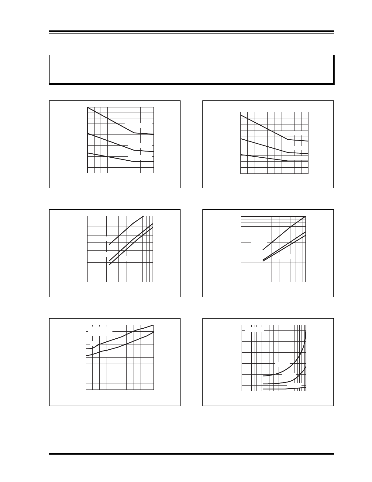
TYPICAL PERFORMANCE CURVES
Note: Unless otherwise indicated, T
A
= +25°C with 4.5V
V
DD
18V.
FIGURE 2-1:
Rise Time vs. Supply
Voltage.
FIGURE 2-2:
Rise Time vs. Capacitive
Load.
FIGURE 2-3:
Propagation Delay Time vs.
Temperature.
FIGURE 2-4:
Fall Time vs. Supply
Voltage.
FIGURE 2-5:
Fall Time vs. Capacitive
Load.
FIGURE 2-6:
Supply Current vs.
Capacitive Load.
Note:
The graphs and tables provided following this note are a statistical summary based on a limited number of
samples and are provided for informational purposes only. The performance characteristics listed herein
are not tested or guaranteed. In some graphs or tables, the data presented may be outside the specified
operating range (e.g., outside specified power supply range) and therefore outside the warranted range.
5
7
9
11
13
15
SUPPLY VOLTAGE (V)
C = 2200 pF
L
120
100
80
60
40
20
0
TIME (nsec)
C = 4700 pF
L
C = 10,000 pF
L
V = 12V
DD
V = 5V
DD
60
40
20
10
1000
10,000
CAPACITIVE LOAD (pF)
V = 18V
DD
80
100
TIME (nsec)
50
40
30
20
10
0
–60
–20
20
60
100
140
TA (°C)
DELAY TIME (nsec)
D1
t
D2
t
C = 2200 pF
L
V = 18V
DD
5
7
9
11
13
15
SUPPLY VOLTAGE (V)
C = 2200 pF
L
TIME (nsec)
C = 4700 pF
L
C = 10,000 pF
L
100
80
60
40
20
0
60
40
20
10
1000
10,000
CAPACITIVE LOAD (pF)
TIME (nsec)
V = 18V
DD
80
100
V = 12V
DD
V = 5V
DD
0
100
1000
10,000
CAPACITIVE LOAD (pF)
SUPPLY CURRENT (mA)
84
70
56
42
28
14
0
500 kHz
200 kHz
20 kHz
V = 15V
DD
TC4420M/TC4429M
DS21933B-page 6
2005-2012 Microchip Technology Inc.
Note: Unless otherwise indicated, T
A
= +25°C with 4.5V
V
DD
18V.
FIGURE 2-7:
Rise and Fall Times vs.
Temperature.
FIGURE 2-8:
Propagation Delay Time vs.
Supply Voltage.
FIGURE 2-9:
Supply Current vs.
Frequency.
FIGURE 2-10:
High-State Output
Resistance vs. Supply Voltage.
FIGURE 2-11:
Effect of Input Amplitude on
Propagation Delay.
FIGURE 2-12:
Low-State Output
Resistance vs. Supply Voltage.
–60
–20
20
60
100
140
TA (°C)
t
RISE
t
50
40
30
20
10
0
TIME (nsec)
C = 2200 pF
V = 18V
DD
FALL
L
65
60
55
50
45
40
35
DELAY TIME (nsec)
4
6
8
10
12
14
16
18
SUPPLY VOLTAGE (V)
t
D2
t
D1
100
0
0
100
1000
10,000
FREQUENCY (kHz)
SUPPLY CURRENT (mA)
10
1000
18V
10V
5V
C = 2200 pF
L
5
4
3
2
5
9
13
SUPPLY VOLTAGE (V)
R ( )
Ω
OUT
100 mA
50 mA
10 mA
7
11
15
200
160
120
80
40
0
DELAY TIME (nsec)
5 6 7
11
13
15
LOAD = 2200 pF
INPUT 2.4V
INPUT 3V
INPUT 5V
INPUT 8V AND 10V
8
9 10
12
14
V (V)
DD
2.5
2
1.5
1
5
9
13
SUPPLY VOLTAGE (V)
R ( )
Ω
OUT
100 mA
50 mA
10 mA
7
11
15
2005-2012 Microchip Technology Inc.
DS21933B-page 7
TC4420M/TC4429M
Note: Unless otherwise indicated, T
A
= +25°C with 4.5V
V
DD
18V.
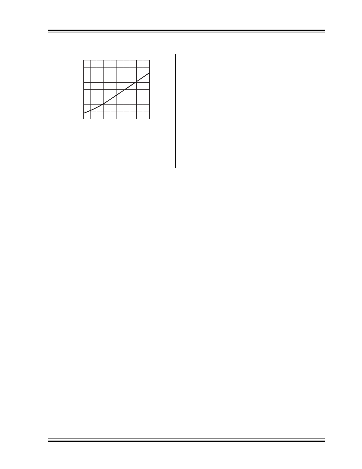
FIGURE 2-13:
Crossover Energy*.
4
3
2
1
0
Crossover Area (A•S) x 10
-8
5
6
7
11
13
15
8
9 10
12
14
SUPPLY VOLTAGE (V)
* The values on this graph represent the loss seen
by the driver during one complete cycle. For a
single transition, divide the value by 2.

TC4420M/TC4429M
DS21933B-page 8
2005-2012 Microchip Technology Inc.
3.0
PIN DESCRIPTIONS
The descriptions of the pins are listed in
Table 3-1
.
3.1
Supply Input (V
DD
)
The V
DD
input is the bias supply for the MOSFET driver
and is rated for 4.5V to 18V with respect to the ground
pins. The V
DD
input should be bypassed to ground with
a local ceramic capacitor. The value of the capacitor
should be chosen based on the capacitive load that is
being driven. A minimum value of 1.0 µF is suggested.
3.2
Control Input
The MOSFET driver input is a high-impedance,
TTL/CMOS-compatible input. The input circuitry of the
TC4420M/TC4429M MOSFET driver also has a
“speed-up” capacitor. This helps to decrease the prop-
agation delay times of the driver. Because of this, input
signals with slow rising or falling edges should not be
used, as this can result in double-pulsing of the
MOSFET driver output.
3.3
CMOS Push-Pull Output
The MOSFET driver output is a low-impedance,
CMOS, push-pull style output capable of driving a
capacitive load with 6.0A peak currents. The MOSFET
driver output is capable of withstanding 1.5A peak
reverse currents of either polarity.
3.4
Ground
The ground pins are the return path for the bias current
and the high peak currents that discharge the load
capacitor. The ground pins should be tied into a ground
plane or have very short traces to the bias supply
source return.
TABLE 3-1:
PIN FUNCTION TABLE
Pin No.
8-Pin CERDIP
Symbol
Description
1
V
DD
Supply input, 4.5V to 18V
2
INPUT
Control input, TTL/CMOS compatible input
3
NC
No Connection
4
GND
Ground
5
GND
Ground
6
OUTPUT
CMOS push-pull output
7
OUTPUT
CMOS push-pull output
8
V
DD
Supply input, 4.5V to 18V
2005-2012 Microchip Technology Inc.
DS21933B-page 9
TC4420M/TC4429M
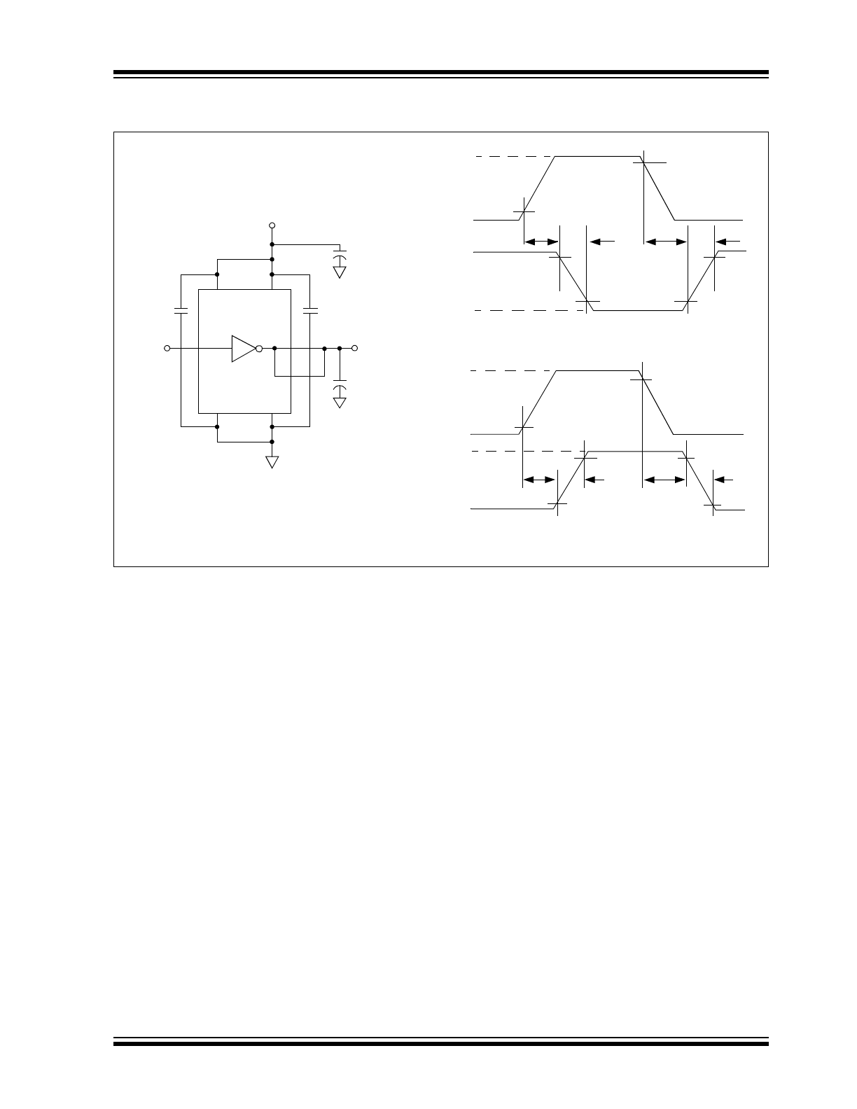
4.0
APPLICATIONS INFORMATION
FIGURE 4-1:
Switching Time Test Circuits.
Inverting Driver
Non-Inverting Driver
Input
t
D1
t
F
t
R
t
D2
Input: 100 kHz,
square wave,
t
RISE
= t
FALL
10 ns
Output
Input
Output
t
D1
t
F
t
R
t
D2
+5V
10%
90%
10%
90%
10%
90%
+18V
0V
90%
10%
10%
10%
90%
+5V
+18V
0V
0V
0V
90%
2
6
7
5
4
1
8
C
L
= 2,500 pF
0.1 µF
4.7 µF
Input
V
DD
= 18V
Output
0.1 µF
TC4420M
TC4429M
TC4420M/TC4429M
DS21933B-page 10
2005-2012 Microchip Technology Inc.
5.0
PACKAGING INFORMATION
5.1
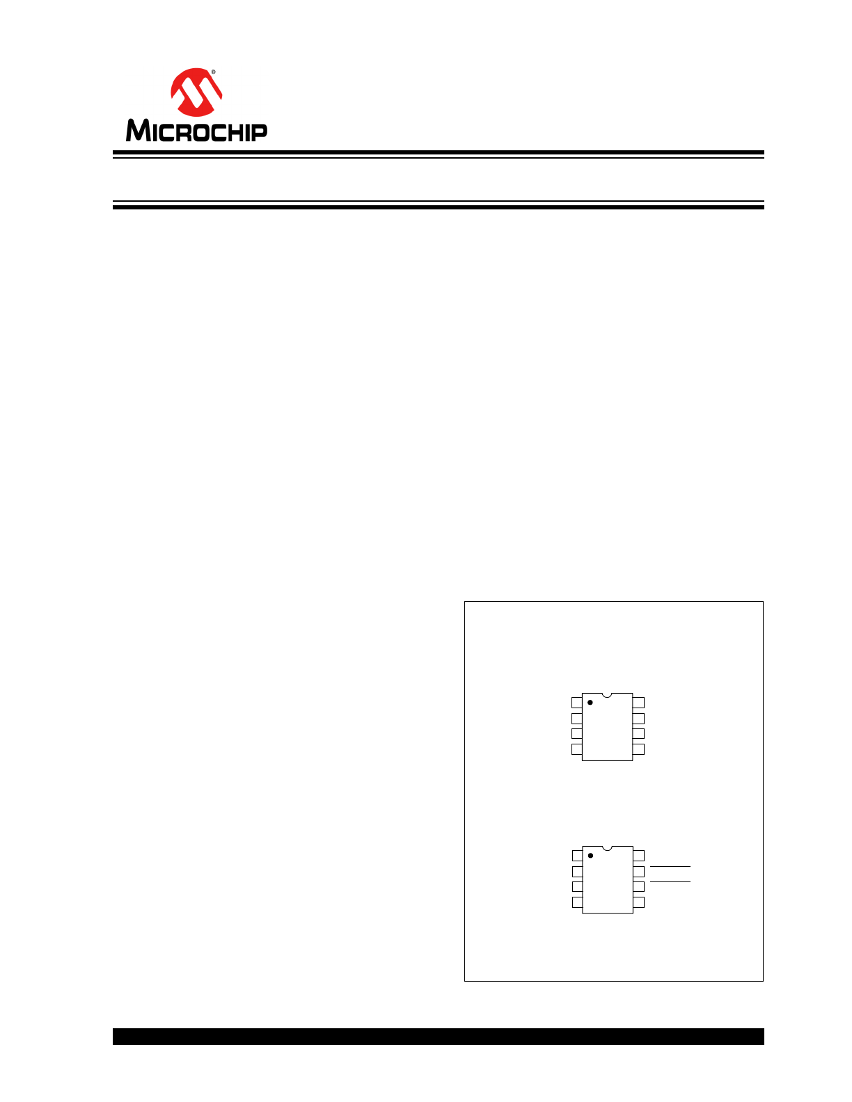
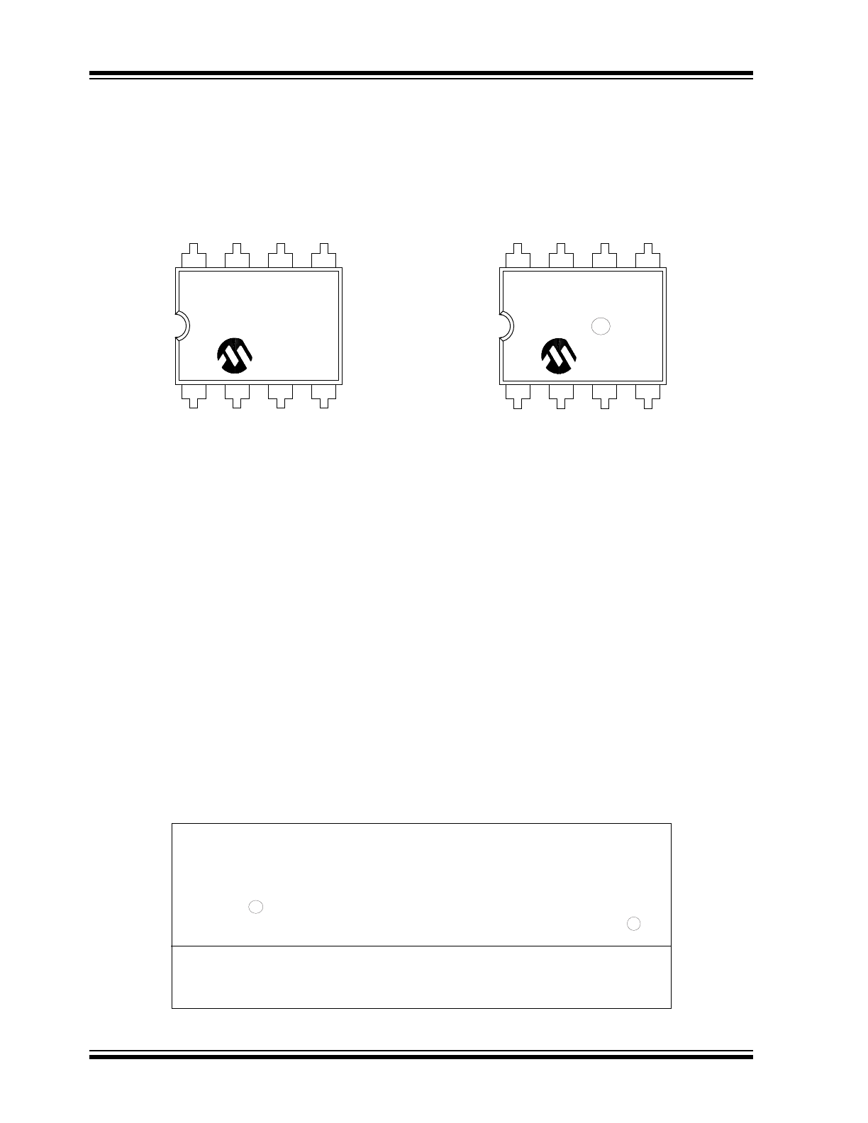
Package Marking Information
Note:
In the event the full Microchip part number cannot be marked on one line, it will
be carried over to the next line, thus limiting the number of available
characters for customer-specific information.
8-Lead CERDIP (.300”)
Example
XXXXXNNN
XXXXXXXX
YYWW
TC4420
MJA 256
1143
Legend: XX...X Customer-specific information
Y Year code (last digit of calendar year)
YY Year code (last 2 digits of calendar year)
WW Week code (week of January 1 is week ‘01’)
NNN Alphanumeric traceability code
Pb-free JEDEC designator for Matte Tin (Sn)
* This package is Pb-free. The Pb-free JEDEC designator ( )
can be found on the outer packaging for this package.
3
e
3
e
3
e