
2002-2016 Microchip Technology Inc.
DS20001418E-page 1
TC4404/TC4405
Features
• Independently Programmable Rise and Fall Times
• Low Output Impedance: 7
Typical
• High Speed t
R
, t
F
: <30 ns with 1000 pF Load
• Short Delay Times: <30 ns
• Wide Operating Range: 4.5V to 18V
• Latch-Up Protected: withstands > 500 mA
Reverse Current (Either Polarity)
• Input Withstands Negative Swings up to -5V
Applications
• Motor Controls
• Driving Bipolar Transistors
• Driver for Non-Overlapping Totem Poles
• Reach-Up/Reach-Down Driver
General Description
The TC4404/TC4405 are CMOS buffer-drivers
constructed with complementary MOS outputs, where
the drains of the totem-pole output have been left
separated so that individual connections can be made
to the pull-up and pull-down sections of the output. This
allows the insertion of drain-current-limiting resistors in
the pull-up and/or pull-down sections, allowing the user
to define the rates of rise and fall for a capacitive load.
It also enables a reduced output swing, if driving a
resistive load, or limiting base current when driving a
bipolar transistor. Minimum rise and fall times, with no
resistors, will be less than 30 ns for a 1000 pF load.
For driving MOSFETs in motor-control applications,
where slow-ON/fast-OFF operation is desired, these
devices are superior to the previously used technique
of adding a diode-resistor combination between the
driver output and the MOSFET, because they allow
accurate control of turn-on, while maintaining fast
turn-off and maximum noise immunity for an OFF
device.
When used to drive bipolar transistors, these drivers
maintain the high speeds common to other Microchip
drivers. They allow insertion of a base current-limiting
resistor, while providing a separate half-output for fast
turn-off. By proper positioning of the resistor, either
NPN or PNP transistors can be driven.
For driving many loads in low-power regimes, these
drivers require significantly less power at higher
frequencies and can be helpful in meeting low-power
budgets as they eliminate shoot-through currents in the
output stage.
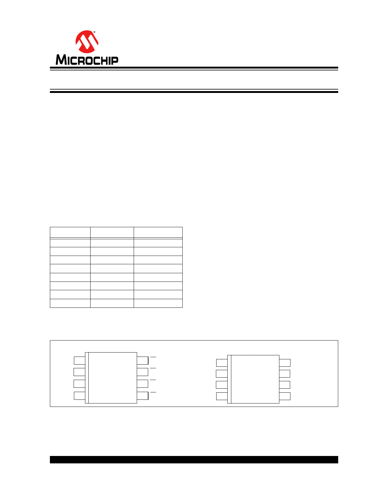
Package Type
TABLE 1:
DEVICE SELECTION TABLE
Part Number
Package
Temp. Range
TC4404COA
8-Lead SOIC
0°C to +70°C
TC4404CPA
8-Lead PDIP
0°C to +70°C
TC4404EOA
8-Lead SOIC
-40°C to +85°C
TC4404EPA
8-Lead PDIP
-40°C to +85°C
TC4405COA
8-Lead SOIC
0°C to +70°C
TC4405CPA
8-Lead PDIP
0°C to +70°C
TC4405EOA
8-Lead SOIC
-40°C to +85°C
TC4405EPA
8-Lead PDIP
-40°C to +85°C
4
5
B BOTTOM
GND
3
6
B TOP
IN B
2
7
A BOTTOM
IN A
1
8
V
DD
A TOP
4
5
B BOTTOM
GND
3
6
B TOP
IN B
2
7
A BOTTOM
IN A
1
8
V
DD
A TOP
TC4405
8-Lead PDIP/SOIC
TC4404
1.5A Dual Open-Drain MOSFET Drivers
TC4404/TC4405
DS20001418E-page 2
2002-2016 Microchip Technology Inc.
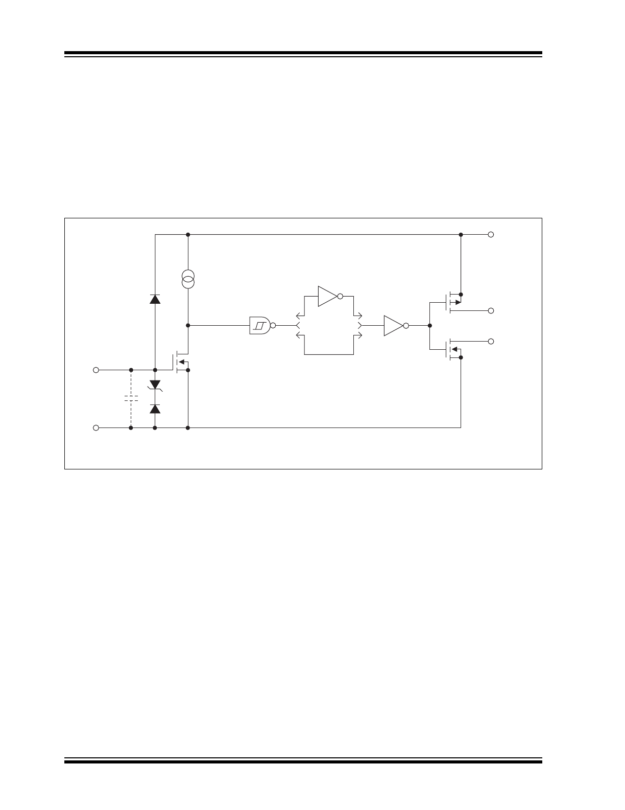
Because neither drain in an output is dependent on the
other, these devices can also be used as open-drain
buffer/drivers where both drains are available in one
device, thus minimizing chip count. Unused open
drains should be returned to the supply rail so that their
device sources are connected (pull-downs to ground,
pull-ups to V
DD
), to prevent static damage. In addition,
in situations where timing resistors or other means of
limiting crossover currents are used, like drains from
drivers A and B, they may be paralleled for greater
current carrying capacity.
These devices are built to operate in the most
demanding electrical environments. They will not
latch-up under any conditions within their power and
voltage ratings; they are not subject to damage when
up to 5V of noise spiking of either polarity occurs on
their ground pin; and they can accept, without damage
or logic upset, up to 0.5A of reverse current (of either
polarity) being forced back into their outputs. All
terminals are fully protected against up to 2 kV (HBM)
of electrostatic discharge.
Functional Block Diagram
Input
GND
Effective
Input
C ≤ 12 pF
300 mV
V
DD
Pull-Up
Pull-Down
2 (3)
A (B)
8 (6)
7 (5)
4
1
TC4404
Inverting
TC4405
Noninverting
4.7V
2002-2016 Microchip Technology Inc.
DS20001418E-page 3
TC4404/TC4405
1.0
ELECTRICAL
CHARACTERISTICS
Absolute Maximum Ratings †
Supply Voltage .....................................................+22V
Power Dissipation (T
A
70°C)
PDIP..................................................... 730 mW
SOIC .................................................... 470 mW
Operating Temperature Range
C Version ........................................ 0°C to +70°C
E Version...................................... -40°C to +85°C
Storage Temperature Range.............. -65°C to +150°C
† Notice:
Stresses above those listed under “Absolute
Maximum Ratings” may cause permanent damage to
the device. This is a stress rating only and functional
operation of the device at those or any other conditions
above those indicated in the operational sections of this
specification is not intended. Exposure to maximum
rating conditions for extended periods may affect
device reliability.
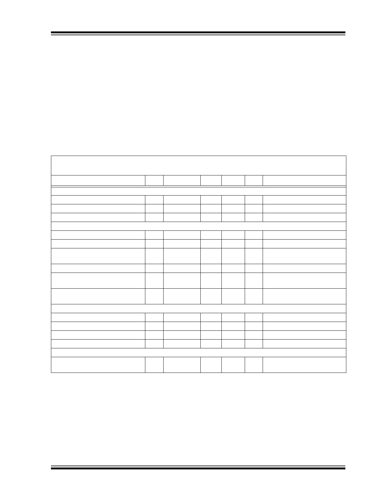
DC CHARACTERISTICS
Electrical Characteristics: Unless otherwise specified, all limits apply for typical values at ambient temperature
T
A
= +25°C, with 4.5V
VDD 18V.
Parameter
Sym.
Min.
Typ.
Max.
Units
Conditions
Input
Logic 1, High Input Voltage
V
IH
2.4
—
—
V
Logic 0, Low Input Voltage
V
IL
—
—
0.8
V
Input Current
I
IN
–1
—
1
A
0V
V
IN
V
DD
Output
High Output Voltage
V
OH
V
DD
– 0.025
—
—
V
Low Output Voltage
V
OL
—
—
0.025
V
Output Resistance
R
O
—
7
10
I
OUT
= 10 mA, V
DD
= 18V;
any drain
Peak Output Current (Any Drain)
I
PK
—
1.5
—
A
Duty cycle
2%, t 300 sec
Continuous Output Current
(Any Drain)
I
DC
—
—
100
mA
Latch-Up Protection (Any Drain)
Withstand Reverse Current
I
R
—
> 500
—
mA
Duty cycle
2%, t 300 sec
Switching Time (
Note 1
)
Rise Time
t
R
—
25
30
ns
Figure 4-1
, C
L
= 1000 pF
Fall Time
t
F
—
25
30
ns
Figure 4-1
, C
L
= 1000 pF
Delay Time
t
D1
—
15
30
ns
Figure 4-1
, C
L
= 1000 pF
Delay Time
t
D2
—
32
50
ns
Figure 4-1
, C
L
= 1000 pF
Power Supply
Power Supply Current
I
S
—
—
—
—
4.5
0.4
mA
V
IN
= 3V (both inputs)
V
IN
= 0V (both inputs)
Note 1: Switching times ensured by design.
TC4404/TC4405
DS20001418E-page 4
2002-2016 Microchip Technology Inc.
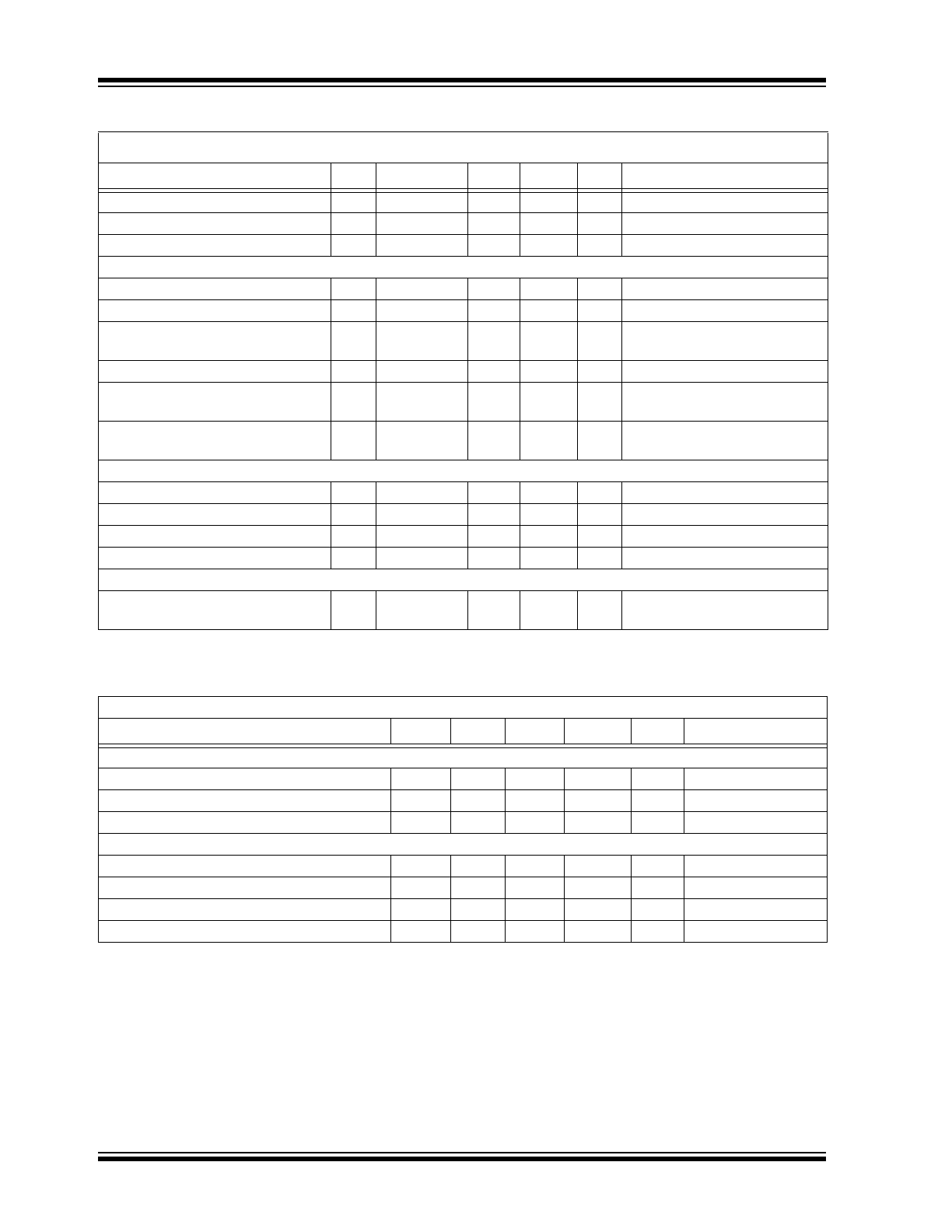
DC CHARACTERISTICS (OVER OPERATING TEMPERATURE RANGE)
Electrical Characteristics: Unless otherwise indicated, operating temperature range with 4.5V
V
DD
18V.
Parameter
Sym.
Min.
Typ.
Max.
Units
Conditions
Logic 1, High Input Voltage
V
IH
2.4
—
—
V
Logic 0, Low Input Voltage
V
IL
—
—
0.8
V
Input Current
I
IN
–10
—
10
A
0V
V
IN
V
DD
Output
High Output Voltage
V
OH
V
DD
– 0.025
—
—
V
Low Output Voltage
V
OL
—
—
0.025
V
Output Resistance
R
O
—
9
12
I
OUT
= 10 mA, V
DD
= 18V;
any drain
Peak Output Current (Any Drain)
I
PK
—
1.5
—
A
Duty cycle
2%, t 300 sec
Continuous Output Current
(Any Drain)
I
DC
—
—
100
mA
Latch-Up Protection (Any Drain)
Withstand Reverse Current
I
R
—
> 500
—
mA
Duty cycle
2%, t 300 sec
Switching Time (
Note 1
)
Rise Time
t
R
—
—
40
ns
Figure 4-1
, C
L
= 1000 pF
Fall Time
t
F
—
—
40
ns
Figure 4-1
, C
L
= 1000 pF
Delay Time
t
D1
—
—
40
ns
Figure 4-1
, C
L
= 1000 pF
Delay Time
t
D2
—
—
60
ns
Figure 4-1
, C
L
= 1000 pF
Power Supply
Power Supply Current
I
S
—
—
—
—
8
0.6
mA
V
IN
= 3V (both inputs)
V
IN
= 0V (both inputs)
Note 1: Switching times ensured by design.
TEMPERATURE SPECIFICATIONS
Electrical Specifications: Unless otherwise noted, all parameters apply with 4.5V
V
DD
18V.
Parameters
Sym.
Min.
Typ.
Max.
Units
Conditions
Temperature Ranges
Operating Temperature Range, C Version
T
A
0
—
+70
°C
Operating Temperature Range, E Version
T
A
-40
—
+85
°C
Storage Temperature Range
T
A
-65
—
+150
°C
Package Thermal Resistances
Thermal Resistance, 8-Lead PDIP
JA
—
+94
—
°C/W
Thermal Resistance, 8-Lead PDIP
JC
—
+45
—
°C/W
Thermal Resistance, 8-Lead SOIC
JA
—
+163
—
°C/W
Thermal Resistance, 8-Lead SOIC
JC
—
+42
—
°C/W
2002-2016 Microchip Technology Inc.
DS20001418E-page 5
TC4404/TC4405
2.0
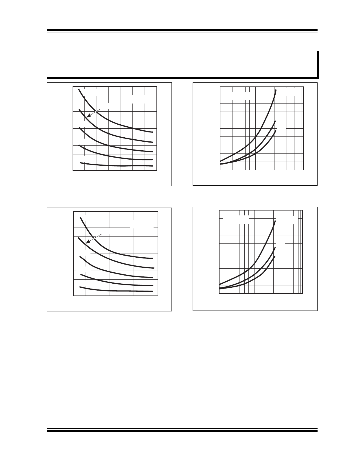
TYPICAL PERFORMANCE CURVES
FIGURE 2-1:
Rise Time vs. Supply
Voltage.
FIGURE 2-2:
Fall Time vs. Supply
Voltage.
FIGURE 2-3:
Rise Time vs. Capacitive
Load.
FIGURE 2-4:
Fall Time vs. Capacitive
Load.
Note:
The graphs and tables provided following this note are a statistical summary based on a limited number of
samples and are provided for informational purposes only. The performance characteristics listed herein
are not tested or guaranteed. In some graphs or tables, the data presented may be outside the specified
operating range (e.g., outside specified power supply range) and therefore outside the warranted range.
4
14
16
18
100 pF
470 pF
2200 pF
1500 pF
100
80
60
40
20
0
1000 pF
4
6
8
14
16
18
100 pF
470 pF
1000 pF
2200 pF
1500 pF
100
80
60
40
20
0
100
1000
10,000
10V
15V
100
80
60
40
20
0
T
A
= +25°C
T
A
= +25°C
T
A
= +25°C
V
DD
= 5V
1
1
1
1
V
DD
t
RI
SE
(n
s)
4
14
16
18
100 pF
470 pF
2200 pF
1500 pF
100
80
60
40
20
0
1000 pF
4
6
8
14
16
18
100 pF
470 pF
1000 pF
2200 pF
1500 pF
100
80
60
40
20
0
100
1000
10,000
10V
15V
100
80
60
40
20
0
T
A
= +25°C
T
A
= +25°C
T
A
= +25°C
V
DD
= 5V
1
1
1
1
V
DD
t
FA
L
L
(ns)
t
RIS
E
(ns)
C
LOAD
(pF)
4
14
16
18
100 pF
470 pF
2200 pF
1500 pF
100
80
60
40
20
0
1000 pF
4
6
8
14
16
18
100 pF
470 pF
1000 pF
2200 pF
1500 pF
100
80
60
40
20
0
100
1000
10000
10V
15V
100
80
60
40
20
0
T
A
= +25°C
T
A
= +25°C
T
A
= +25°C
V
DD
= 5V
1
1
1
1
t
FA
L
L
(ns)
C
LOAD
(pF)
60
50
40
30
20
10
4
6
8
14
16
18
-55 -35 -15 5 25 45 65 85 105 125
60
50
40
30
20
10
100
1000
10000
100
80
60
40
20
0
10V
15V
t
D1
T
A
= +25°C
t
D2
V
DD
= 5V
C
LOAD
= 1000 pF
V
DD
= 17.5V
C
LOAD
= 1000 pF
T
A
= +25°C
t
FALL
t
RISE
1
1
TC4404/TC4405
DS20001418E-page 6
2002-2016 Microchip Technology Inc.
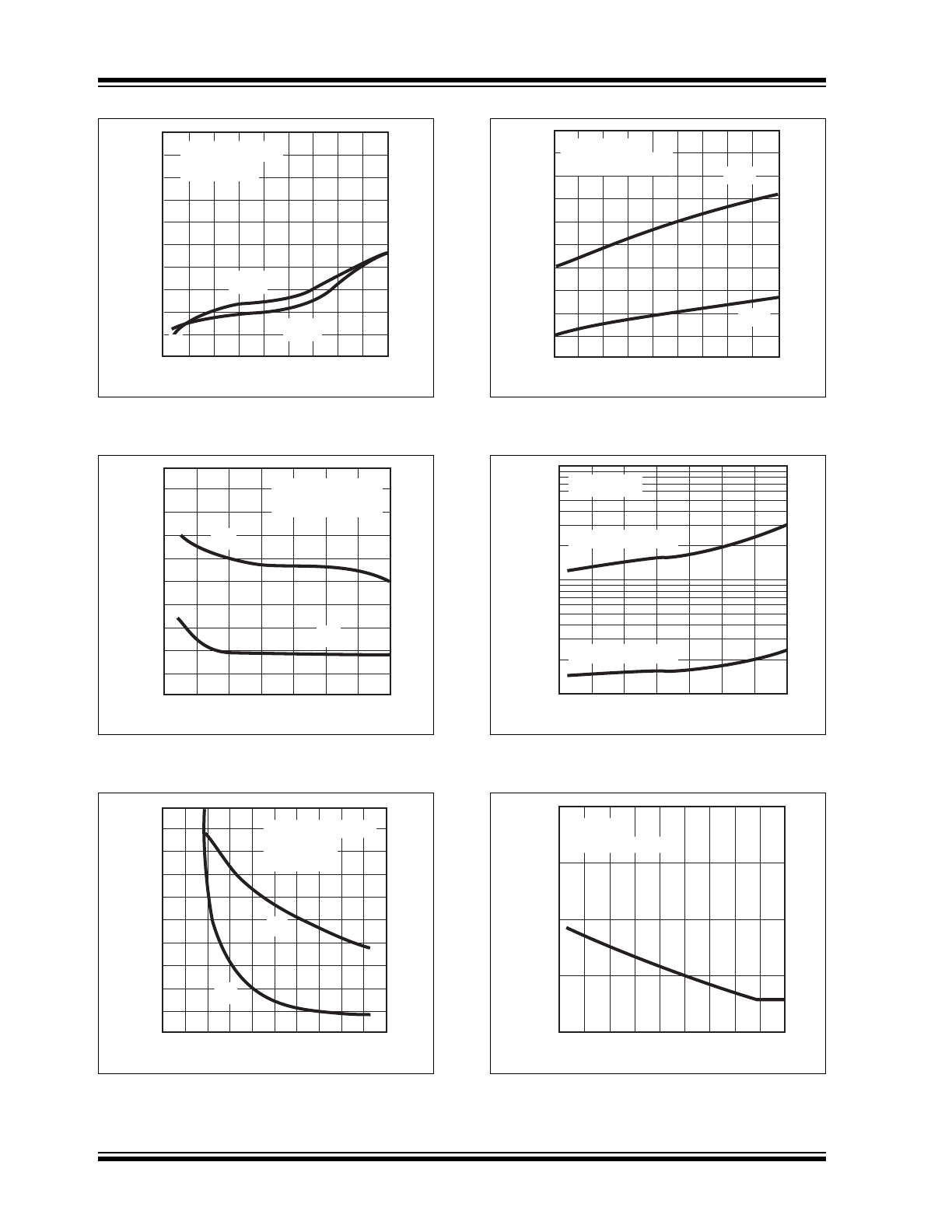
FIGURE 2-5:
Rise and Fall Times vs.
Temperature.
FIGURE 2-6:
Propagation Delay vs.
Supply Voltage.
FIGURE 2-7:
Effect of Input Amplitude on
Delay Time.
FIGURE 2-8:
Propagation Delay Time vs.
Temperature.
FIGURE 2-9:
Quiescent Supply Current
vs. Voltage.
FIGURE 2-10:
Quiescent Supply Current
vs. Temperature.
60
50
40
30
20
10
4
6
8
14
16
18
-55 -35 -15 5 25 45 65 85 105125
60
50
40
30
20
10
100
1000
10000
100
80
60
40
20
0
10V
15V
t
D1
T
A
= +25°C
t
D2
V
DD
= 5V
C
LOAD
= 1000 pF
V
DD
= 17.5V
C
LOAD
= 1000 pF
T
A
= +25°C
t
FALL
t
RISE
1
1
Ti
m
e
(
n
s)
Temperature
60
50
40
30
20
10
4
6
8
14
16 18
-55 -35 -15 5 25 45 65 85 105 125
60
50
40
30
20
10
100
1000
10000
100
80
60
40
20
0
10V
15V
t
D1
T
A
= +25°C
t
D2
V
DD
= 5V
C
LOAD
= 1000 pF
V
DD
= 17.5V
C
LOAD
= 1000 pF
T
A
= +25°C
t
FALL
t
RISE
1
1
V
DD
De
la
y T
ime
(n
s)
-55 -35 -15 5 25 45 65 85 105 125
4
18
6
8
10
12
14
16
60
50
40
30
20
10
10
B
I
= 1
B
I
= 0
0
2
4
6
8
1
0.1
t
D1
T
A
= +25°C
t
D2
C
LOAD
= 1000pF
V
DD
= 10V
T
A
= +25°C
V
DD
= 17.5V
V
LOAD
= 1000pF
t
D1
t
D2
60
50
40
30
20
10
10
Delay T
ime
(n
s)
V
DRIVE
(V)
--55 -35 -15 5 25 45 65 85 105125
4
18
6
8
10
12
14
16
60
50
40
30
20
10
10
B
I
= 1
B
I
= 0
0
2
4
6
8
1
0.1
t
D1
T
A
= +25°C
t
D2
C
LOAD
= 1000pF
V
DD
= 10V
T
A
= +25°C
V
DD
= 17.5V
V
LOAD
= 1000pF
t
D1
t
D2
60
50
40
30
20
10
10
Delay T
ime (ns)
Temperature
-55 -35 -15 5 25 45 65 85 105 125
44
18
6
8
10
12
14
16
60
50
40
30
20
10
10
BRWK IQSXWV = 1
BRWK IQSXWV = 0
0
2
4
6
8
1
0.1
t
D1
T
A
= +25°C
t
D2
C
LOAD
= 1000pF
V
DD
= 10V
T
A
= +25°C
V
DD
= 17.5V
V
LOAD
= 1000pF
t
D1
t
D2
60
50
40
30
20
10
10
V
DD
I
QU
IESCEN
T
(mA)
--55 -35 -15 5 25 45 65 85 105125
44.0
3.5
3.0
2.5
2.0
4
6
8
14
16
18
25
20
15
10
5
4
6
8
14
16 18
25
20
15
10
5
W
@ T
J
= +150°C
T @ +25°C
T @ +25°C
W
@ T
J
= +150°C
V
DD
= 18V
BRWK IQSXWV = 1
1
1
1
1
I
QU
IESC
E
N
T
(mA)
Temperature
2002-2016 Microchip Technology Inc.
DS20001418E-page 7
TC4404/TC4405
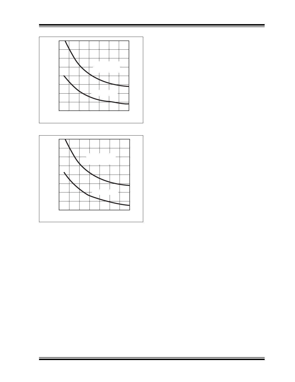
FIGURE 2-11:
Pull-Up Output Resistance.
FIGURE 2-12:
Pull-Down Output
Resistance.
-55 -35 -15 5 25 45 65 85 105 125
4.0
3.5
3.0
2.5
2.0
4
6
8
14
16
18
25
20
15
10
5
4
6
8
14
16 18
25
20
15
10
5
W
@ T
J
= +150°C
T @ +25°C
T\S @ +25°C
WRUVW&DVH
@ T
J
= +150°C
V
DD
= 18V
B
I
= 1
1
1
1
1
V
DD
R
DS(
O
N
)
(
)
-55 -35 -15 5 25 45 65 85 105 125
4.0
3.5
3.0
2.5
2.0
4
6
8
14
16
18
25
20
15
10
5
4
6
8
14
16 18
25
20
15
10
5
WRUVW&DVH
@ T
J
= +150°C
T\S @ +25°C
T
@ +25°C
W
@ T
J
= +150°C
V
DD
= 18V
B
I
= 1
1
1
1
1
V
DD
R
DS
(ON
)
(
)
TC4404/TC4405
DS20001418E-page 8
2002-2016 Microchip Technology Inc.
3.0
PIN DESCRIPTIONS
The descriptions of the pins are listed in
Table 3-1
.
TABLE 3-1:
PIN FUNCTION TABLE
8-Lead PDIP/SOIC
Symbol
Description
1
V
DD
Supply Input, 4.5V to 18V
2
IN A
Control Input A, TTL/CMOS compatible input
3
IN B
Control Input B, TTL/CMOS compatible input
4
GND
Ground
5
B BOTTOM Output B, pull-down
6
B TOP
Output B, pull-up
7
A BOTTOM Output A, pull-down
8
A TOP
Output A, pull-up
2002-2016 Microchip Technology Inc.
DS20001418E-page 9
TC4404/TC4405
4.0
APPLICATIONS INFORMATION
4.1
Circuit Layout Guidelines
Long power supply and ground traces should be
avoided as the added inductance causes unwanted
voltage transients. Power and ground planes should be
used wherever possible.
In addition, it is advisable that low ESR (Equivalent
Series Resistance) bypass capacitors (4.7 µF or 10 µF
tantalum) be placed as close to the driver as possible.
In order to minimize the length of the output trace, the
driver should be physically located as close as possible
to the device it is driving.
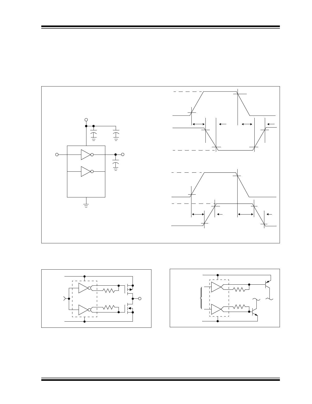
FIGURE 4-1:
Switching Time Test Circuit.
4.2
Typical Applications
FIGURE 4-2:
Zero Crossover Current
Totem-Pole Switch.
FIGURE 4-3:
Driving Bipolar Transistors.
C
L
= 1000 pF
+5V
10%
90%
10%
90%
10%
90%
18V
0V
0V
90%
10%
10%
10%
90%
+5V
18V
0V
0V
90%
4
2
8.7
1
1
2
0.1 µF
4.7 µF
Inverting Driver
Noninverting Driver
Input
V
DD
= 18V
Input
Output
t
D1
t
F
t
R
t
D2
Input: 100 kHz,
square wave,
t
RISE =
t
FALL
10 ns
Output
Input
Output
t
D1
t
F
t
R
t
D2
R
T
R
T
V
DD
(4.5V - 18V)
From TTL
GND
V
OUT
TC4404
GND
TC4405
V
DD
(4.5V - 18V)
From TTL
R
IB
R
IB
TC4404/TC4405
DS20001418E-page 10
2002-2016 Microchip Technology Inc.
FIGURE 4-4:
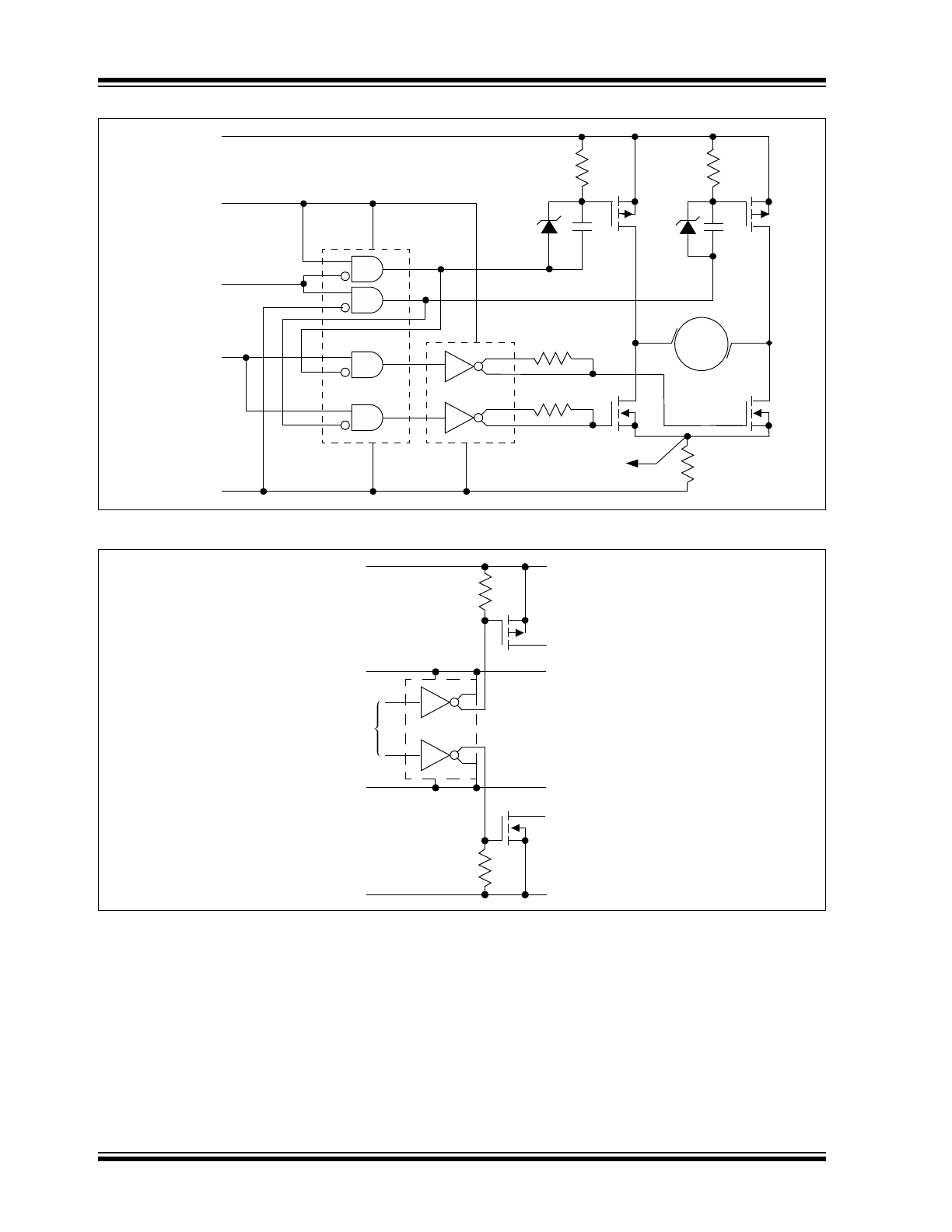
Servo Motor Control.
FIGURE 4-5:
Reach-Up and Reach-Down Driving.
47 k
0.1µF
15V
15V
R
T
I
SENSE
+24V
+12V
Direction
(TTL Level)
Speed
(PWM)
Motor
TC4404
TC4469
GND
47 k
0.1µF
R
T
From TTL
-12V
+12V
+5V
GND
-12V
+12V
+5V
GND
Switched
+12V
Switched
-12V
TC4404